 Open Access Article
 This Open Access Article is licensed under a Creative Commons Attribution-Non Commercial 3.0 Unported Licence
Transverse charge transport through DNA oligomers in large-area molecular junctions
Ilias Katsouras*ab,
Claudia Piliegoa,
Paul W. M. Bloma and
Dago M. de Leeuwab
aMax Planck Institute for Polymer Research, Ackermannweg 10, Mainz, 55128, Germany. E-mail: katsouras@mpip-mainz.mpg.de; Tel: +49 6131379721
bZernike Institute for Advanced Materials, University of Groningen, Nijenborgh 4, Groningen, 9747AG, The Netherlands
First published on 6th August 2013
Abstract
We investigate the nature of charge transport in deoxyribonucleic acid (DNA) using self-assembled layers of DNA in large-area molecular junctions. A protocol was developed that yields dense monolayers where the DNA molecules are not standing upright, but are lying flat on the substrate. As a result the charge transport is measured not along the DNA molecules but in the transverse direction, across their diameter. The electrical transport data are consistent with the derived morphology. We demonstrate that the charge transport mechanism through DNA is identical to non-resonant tunneling through alkanethiols with identical length, classifying DNA as a dielectric.
Introduction
Deoxyribonucleic acid (DNA) has been established as the most important biological polymer, since it carries genetic information.1,2 The answer to the question why such a complex molecule should be used in a field so different from the role that nature has assigned to it can be sought in its unique features, which cannot be found in other polymers. DNA possesses complementarity, the self-assembling ability that always leads to the formation of specific hydrogen-bonded base pairs. Thanks to its self-assembling characteristics, which allow it to be highly integrated error-free with no need for microfabrication technologies, DNA is highly interesting as a functional nano-sized material.The DNA molecule can be viewed as a series of nitrogenous bases connected through a sugar-phosphate backbone. DNA in the cell functions as a double-stranded helix of B-form DNA, the structure of which was first determined by Watson and Crick3 and which is reproduced in Fig. 1. The polar sugar-phosphate backbones of each strand form the helical scaffold, with the nitrogenous bases in the interior of the molecule having their planes nearly perpendicular to the helical axis. The diameter of the B-DNA is ∼20 Å.
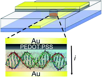 | ||
| Fig. 1 Schematic structure of a large-area molecular junction. A double-stranded helix of B-DNA is lying flat on the bottom gold electrode. The top electrode is a layer of the conducting polymer PEDOT:PSS, a water-based suspension of poly(3,4-ethylenedioxythiophene) and poly(4-styrenesulphonic acid). This interlayer between the DNA layer and the top Au electrode prevents electrical shorts. The transverse charge transport is measured across the DNA molecule. The DNA is self-assembled in vias defined in photoresist to prevent cross talk. The diameter ranges from 5 μm to 100 μm. | ||
The nature of charge transport through DNA remains largely unresolved. DNA allegedly spans the whole spectrum of conductive behavior, having been reported to be an insulator, a semiconductor, a conductor and even a superconductor.4–15 DNA can be synthesized in any desired base sequence with high accuracy. The recognition capability due to complementarity makes DNA a prototype system for self-assembled electronics. However, the ambiguity around DNA's charge transport properties needs to be lifted.
Several experimental techniques, for instance scanning tunneling microscopy (STM)16–18 and conducting probe atomic force microscopy (CP-AFM),19 have been applied to investigate the charge transport along single DNA molecules or bundles thereof.20,21 The large spread in conductivity values may be attributed to the differences in measurement methods and/or to the different configurations that a single DNA molecule can assume in each test bed. In particular, due to the high sensitivity of DNA, the experimental environment is a critical factor for accurate electrical measurements.22–25 To ensure a controlled environment, we have studied an ensemble of DNA molecules self-assembled in a monolayer, using the previously developed technology of large-area molecular junctions.26,27 As schematically shown in Fig. 1, the junction consists of a self-assembled DNA layer sandwiched between two electrodes, enclosed in an insulating matrix defined in photoresist. Processing within the lithographically defined vertical interconnects (vias) prevents both parasitic currents and cross-talk between different junctions. The junctions offer a solvent and stress free environment. Furthermore, since the junctions are sealed, the SAM is protected from contamination.28
For chemical bonding with an Au substrate, DNA molecules are typically modified with a thiol end group that has a high affinity for Au. However, other interactions, such as those between the base pairs and phosphate groups of DNA with the Au substrate, prevail and result in monolayers of poor coverage.28,29 Improved coverage has been reported by passivating the Au substrate with an incomplete monolayer of short alkanethiols.30 The short alkanethiol molecules compete with the weaker nonspecific interactions and prevent the target DNA molecules from binding nonspecifically to the Au surface. However, fabrication of a dense self-assembled monolayer of upright standing DNA molecules on Au remains problematic.31–33
We have investigated the formation of DNA monolayers to develop a procedure for the fabrication of dense films, suitable for electrical characterization. The use of highly passivated Au substrates yielded a low grafting density, resulting in electrically shorted molecular junctions. However, surprisingly, on briefly passivated Au electrodes dense DNA monolayers could be assembled. The obtained monolayers have been characterized by polarization modulation infrared reflection absorption spectroscopy (PM-IRRAS), atomic force microscopy (AFM) and ellipsometry. We show that the coverage depends on the number of base pairs. Ellipsometry measurements show that for optimized films the layer thickness is comparable to the diameter of the DNA molecules, which indicates that the molecules are lying flat on the substrate, as schematically depicted in Fig. 1. The electrical transport, as measured in the large area junctions, is therefore due to transverse conduction through the DNA molecules. We demonstrate that the conductivity and the temperature dependence of the resistance are identical to those of alkanethiols having a length equal to the DNA layer thickness.34 As a result the transverse conduction in DNA is due to non-resonant tunneling, classifying DNA as a dielectric, in agreement with previous reports.4,6,9,10,15,35,36
Experimental
The junctions were formed as described previously.26 On a 4′′ thermally oxidized silicon monitor wafer, patterned bottom Au electrodes were evaporated on a 1 nm Cr adhesion layer. The rms roughness of the bottom contact is about 0.7 nm. Subsequently, a photoresist layer (ma-N 1410, Micro Resist Technology GmbH) was spincoated and patterned by conventional I-line lithography, creating circular vertical interconnects (vias) on top of the bottom electrodes, ranging from 5 μm to 100 μm in diameter. For the passivation, the wafer was immersed in a 2 mM solution of 1-hexanethiol in ethanol. The wafer was subsequently rinsed with ethanol, toluene and propanol, and dried under a N2 stream. The DNA was deposited and a layer of the conducting polymer PEDOT:PSS was spincoated on top. PEDOT:PSS is a water-based suspension of poly(3,4-ethylenedioxythiophene) and poly(4-styrenesulphonic acid). This interlayer between the DNA layer and the top Au electrode prevents electrical shorts. The highly acidic PEDOT:PSS (pH ∼ 1.8) can damage DNA by denaturation.37 Therefore, the solution was neutralized by adding a dilute solution of dimethylaminoethanol. Finally, the junction is finished by evaporating top gold electrodes and using them as a self-aligned mask to etch away the redundant PEDOT:PSS.The DNA oligomers contained 14, 22 and 30 base pairs (14mer, 22mer and 30mer respectively) and were modified with a short alkyl spacer and a thiol termination.38 The DNA oligomers were dissolved in a 1 M phosphate buffer, containing 1 M NaCl, with a final concentration of DNA of 2.5 μM. The wafer was covered with the DNA solution for at least 72 hours. Subsequently, to desalinate the SAM, the wafer was gently rinsed with dilute phosphate buffer and de-ionized water, and dried under a N2 stream.
Current–voltage (I–V) measurements were performed in a home-built probe station using a Keithley 4200 Semiconductor Analyzer Characterization System. The probe station was evacuated for at least 6 hours before the measurements, to remove any water absorbed. Ellipsometric measurements were performed using a V-VASE® ellipsometer (J.A. Woolam Co, Inc). The substrates were prepared by template stripping of Au on 1 × 2 cm glass slides. Ellipsometry samples and molecular junctions were prepared simultaneously from the same solutions. All measurements were performed at the reflection geometry in the spectral range from 350 nm to 800 nm, at an angle of incidence of 65–75°. The index of refraction was taken as 1.5. The layer thickness was determined by averaging at least 2 different measurements on each substrate. The same substrates were used for the PM-IRRAS and AFM characterization.
Results and discussion
We first started from single stranded DNA with 14, 22 and 30 base pairs, each with both a propane- or hexanethiol linker. For passivation we treated the Au substrate with mercaptopropanol, mercaptohexanol, hexanethiol or mercaptoundecanol. The incubation time was typically a day yielding fully covered SAMs. Then the DNA was assembled for about 1 day. The growth is mediated by exchange and the presence of defects. Subsequently the film was hybridized for 24 hours with the complementary strand, both at 65 °C and 88 °C. However, in all cases the electrical transport could not be distinguished from PEDOT:PSS-only diodes. Apparently, the coverage is low, the monolayer is not dense enough and therefore the diodes are electrically shorted.As a next step we prepared the DNA films directly from double stranded DNA. Both single and double thiol terminated linkers were investigated. We varied the incubation time for the passivating molecules from minutes to days. Both without the passivation layer (zero incubation time) and when the incubation time was longer than 1 hour, the electrical transport could not be distinguished from PEDOT:PSS-only diodes. The diodes are shorted because the monolayer is not dense.
Surprisingly, the resistance of diodes fabricated from double-stranded DNA with short incubation times is significantly higher than that of PEDOT:PSS-only diodes. Apparently, a dense monolayer can be formed under these conditions. The higher resistance is a sign of the presence of DNA. We deliberately varied the processing conditions. The optimized fabrication protocol consists of using a passivating molecule that matches the length of the DNA linker, in our case hexanethiol, and an incubation time of about 5 minutes. The coverage of the passivating layer is estimated to be around 60–70%. Then a dense DNA layer is formed. The exact processing window has not yet been fully determined. However in the limiting cases of 0% or 100% coverage of the passivating molecules, only partial coverage of double-stranded DNA is obtained. The DNA layer then is incomplete and not dense. We note that single-stranded DNA does not yield full coverage even when using short incubation times for the passivating molecules. The reason is the hybridization step after monolayer formation. This hybridization step is performed at elevated temperatures, around 65 °C to 88 °C, where desorption of the passivating molecules occurs.39 Preliminary experiments have shown that a dense DNA layer can be formed from single-stranded DNA, using a short incubation time for the passivating molecule provided that the hybridization step is performed at room temperature. However, this procedure has not been employed because the long hybridization time, of up to 5 days, is prohibitive.
The presence of DNA molecules on the substrate has been verified by PM-IRRAS, which is an established analytical technique for the characterization of very thin layers on metal surfaces.40,41 The sample is investigated in reflection geometry under grazing incidence, typically 80°. Polarization modulation is used to enhance the sensitivity and to eliminate disturbing atmospheric absorptions caused by water vapor and CO2. Polarization modulation is based on the different absorption of p- and s-polarized light at large angles of incidence. Ultrathin layers on metal surfaces interact with the p-polarized fraction of light, but not with the s-polarized one. Typical infrared absorption spectra of the self-assembled DNA monolayers of the 14mer, 22mer and 30mer are presented in Fig. 2. The spectra show the characteristic vibrations of the phosphate backbone and of the DNA base pairs,42 which are absent in the control experiment with only the hexanethiol passivation layer.
 | ||
| Fig. 2 PM-IRRAS spectra. The solid lines represent the absorption spectra of the hexanethiol control sample (C6, black) and the self-assembled monolayers of DNA with 14 (red), 22 (green) and 30 (blue) base pairs. The DNA spectra show the characteristic peaks of the DNA bases and the phosphate backbone, which are not present in the control sample. | ||
The microstructure of the DNA films was investigated by AFM. Typical topography images for DNA-14mer, 22mer and 30mer with one hexanethiol linker are presented in Fig. 3. Cross-sections through the topography show patches of about 2 nm in height. The films however are not densely packed. Fig. 3 shows that the coverage increases with the number of base pairs. For the DNA-30mer an almost dense layer is obtained. In general the coverage depends on the number of base pairs, the number of thiol linkers and the preparation protocol, such as the density of the passivation alkanethiol film. Quantification is hampered by the bottom electrode being not atomically smooth. To that end, we performed ellipsometry measurements.
 | ||
| Fig. 3 Topography images of self-assembled layers of a DNA-14mer, 22mer and 30mer with one thiol linker. The scan size is 1 μm2. The rms roughness values of the AFM images are 0.36 nm (14mer), 0.42 nm (22mer) and 0.44 nm (30mer) over an area of 1 μm2. The vertical scale bar is indicated. The images show islands on the Au substrate, whose coverage increases with the number of base pairs. For the DNA-30mer an almost dense layer is obtained. | ||
The measured thickness is presented as a function of the number of base pairs in Fig. 4. The three hybridized DNA molecules, with 14, 22 and 30 base pairs, have a calculated length of 4 nm, 7 nm and 10 nm respectively. Fig. 4 shows that the measured layer thickness is much smaller than the length of the molecules. The molecules therefore are not standing upright. For the DNA molecules with the double linker (blue line) the layer thickness is almost independent of the length of the molecule. Actually, the value corresponds to the diameter of the DNA molecules, of about 2 nm. It can therefore be concluded that we have a fully covered monolayer of molecules, which are not standing upright but are lying flat on the substrate. This is supported by the similar layer thickness of the longest DNA molecule with a single linker. From the ellipsometric measurements (Fig. 4) we estimate a coverage between 75% and 100% for DNA with the double thiol linker and from 50% to about 90% for the single thiol linker. We note that the DNA molecules are presumably lying flat due to the low grafting density on the passivated bottom electrode. The negatively charged DNA molecules repel each other due to electrostatic Coulomb interactions, preventing upright assembly. The dominant Coulomb interaction of the DNA molecules with the gold substrate favors planar adsorption. Although the difference between single thiol and double thiol linkers can be explained on the basis of enhanced interactions with the substrate, the dependence of coverage on the number of base pairs remains unclear.
 | ||
| Fig. 4 Layer thickness from ellipsometry measurements of self-assembled DNA layers, as a function of the number of base pairs. The green and blue lines are for hybridized DNA molecules with a single and double thiol linker. The inset shows schematically the orientation of the hybridized DNA molecules; they are lying flat on the surface. | ||
The DNA oligomers we use here contain up to 30 base pairs. The length of the oligomers is shorter than the persistence length of about 50 nm. Supercoiling is then unlikely. However, we cannot rule out the formation of any in-plane superstructure, such as bundles. AFM and ellipsometry measurements show that the molecules are lying flat. Hence, the in-plane ordering of the DNA chains is not relevant for transverse charge transport across the DNA chains.
Typical J–V characteristics of the DNA-14mer, 22mer and 30mer with one and two thiol linkers, as measured in a large area junction, are presented in Fig. 5a. The current scales linearly with the device area as verified for junctions with diameter between 5 μm and 100 μm. The red curve represents a hexanethiol-only junction, used as a reference. Upon insertion of a DNA layer, the current density decreases. The green lines represent DNA with one thiol linker and the blue lines represent DNA with two thiol linkers. Each data point represents the average value over more than 20 junctions. Fig. 5a shows that the shape of the J–V characteristics is almost invariant. At high bias the current density increases as a power law with the applied field. At low bias, below 1 V, the J–V characteristics are linear.
 | ||
| Fig. 5 Transverse charge transport. (a) Current density as a function of applied voltage, as determined in large-area molecular junctions, for DNA molecules with one (green) and two (blue) thiol linkers. The red line represents a hexanethiol-only junction used as a reference. The current scales linearly with the device area. The diameter of the vias was varied between 5 μm and 100 μm. Each data point is an average value over more than 20 junctions. (b) The extracted normalized resistance as a function of the number of DNA base pairs. The green and blue lines are for hybridized DNA molecules with a single and double hexanethiol linker. The normalized resistance, RS, resistance times area, was calculated at 0.1 V bias where the J–V curves are linear. The red dotted line represents the resistance of the independently measured reference junction of hexanethiol. | ||
Previous experiments have been reviewed.43 A number of researchers have investigated charge transport in various prototypes of DNA and in a number of oligomers synthesized with different base pair sequences and lengths. The electrical transport ranged from the insulator through the semiconductor and the metal to the superconductor. The large scatter in the data might be attributed to different base sequences and lengths, electrode type and contact methods, and measuring conditions including temperature, pH, counter ions, and the amount of water and oxygen.43 We note that in this work we make sure that we measure desalinated and dehydrated DNA. Therefore the charge balancing counter cations do not play a role in the observed electrical behavior in our measurements. The data presented here are averages over 20 junctions. The small parameter spread originates from the solvent-, salt- and water-free environment of large-area molecular junctions. We have shown previously that this test bed yields statistically significant transport data for charge transport through single molecules self-assembled in monolayers.34 The reproducibility is here confirmed for the charge transport through DNA.
The resistance of the DNA monolayers, as extracted at low bias and normalized for the device area (RS, resistance times area), is presented as a function of the number of base pairs in Fig. 5b. The green symbols represent DNA molecules with a single hexanethiol linker and the blue symbols represent DNA molecules with two hexanethiol linkers. In all cases the resistance is higher than that of an independently measured passivating dense layer of hexanethiol as indicated by the red dotted line. The higher resistance is due to the presence of DNA. We note that the resistance is hardly dependent on the length of the DNA molecule. For a dense monolayer with all DNA molecules perpendicular to the substrate, an exponential dependence on length is expected.26,44 Here, however, we observe a change of only a factor of three for the single thiolated DNA molecules. For the double thiolated DNA molecules there is no length dependence at all. The reason is unveiled by the ellipsometry measurements in Fig. 4, which shows that the DNA molecules in the self-assembled monolayer are not standing perpendicular to the substrate but they are lying flat. The charge transport is measured not along the DNA molecule but in the transverse direction, across the molecule. For DNA with the double thiol linker the layer thickness does not depend on the number of base pairs and hence, in good agreement, the resistance is constant. For DNA with a single thiol linker the DNA layers are incomplete (Fig. 3 and 4). The coverage increases by about a factor of 2 with the number of base pairs. This corresponds well to the measured variation of a factor of 3 in resistance. We note that, even at the relatively low coverage of only 50%, electrical characterization in molecular junctions is still possible. The PEDOT:PSS particles, which are typically 50–100 nm in diameter, cannot penetrate into the pinholes.
The resistance value obtained for the DNA layers with double thiol linkers is 4 × 10⁶ Ohm μm2. We showed that the DNA molecules, whose diameter is 2 nm,3 are lying flat on the surface. As a reference for 1-octadecanethiol (C18MT), with a measured SAM thickness of approximately 2.1 nm, a resistance of 3 × 10⁶ Ohm μm2 has been reported.34 A comparison between the J–V curves for DNA 22mer and C18MT is shown in Fig. 6a. A qualitative and quantitative agreement between DNA and C18MT is observed. The two curves have the same shape and absolute values of current density. Charge transport has previously been investigated in large-area molecular junctions of alkanes and para-phenylene oligomers.44 Their J(V,T) characteristics have been quantitatively interpreted. The resistance of the junction is factorized with the resistance of PEDOT:PSS. The power-law dependence on both temperature and bias stems from PEDOT:PSS. The molecular contribution is an exponential length dependent pre-factor that originates from non-resonant tunneling. The measurements of normalized resistance as a function of temperature presented in Fig. 6b verify that the temperature dependence of DNA 22mer is identical to C18MT. Furthermore, the resistance of DNA 22mer matches the value of the C18MT SAM, which has an almost identical thickness. The experimental data show that the charge transport through DNA and C18MT is identical, which in the case of C18MT was established to originate from non-resonant tunneling.44,45
 | ||
| Fig. 6 (a) Comparison of the current density of junctions containing DNA 22mer and 1-octadecanethiol (C18MT). The diameter of the vias was varied between 5 μm and 100 μm. Each data point is an average value over more than 20 junctions. (b) Normalized resistance as a function of temperature for DNA 22mer and C18MT. Each data point is an average value over 8 junctions with diameters ranging between 5 μm and 50 μm. The black line represents PEDOT:PSS-only junctions (data reproduced from ref. 45). | ||
Conclusions
We have investigated the fabrication of self-assembled layers of hybridized B-DNA consisting of 14, 22 and 30 base pairs, modified with either one or two short alkyl spacers with a thiol termination. A passivating alkanethiol layer, matching the length of the DNA thiol linker, was used. When the thiol coverage is around 60–70%, a dense DNA layer is subsequently formed. The presence of DNA on the substrate has been verified by PM-IRRAS and AFM. We confirm, from ellipsometry measurements, that dense monolayers of hybridized DNA molecules are obtained, which, however, are lying flat on the substrate. The derived morphology explains the electrical transport, as determined in large-area molecular junctions. We measure the charge transport not along the molecules but in the transverse direction, across their diameter. This automatically implies that the normalized resistance is identical for all fully covered layers. The experimental data show that the charge transport mechanism through DNA is due to non-resonant tunneling and that DNA behaves as a dielectric.Acknowledgements
We greatly acknowledge Prof. A. Herrmann, Dr D. K. Prusty and P. Gordiichuk for providing the DNA oligomers. We thank J. Vorenkampp for the acquisition of the PM-IRRAS spectra and Dr X. Zhou for the AFM data. We would like to thank J. Harkema for the technical assistance and the Zernike Institute for Advanced Materials and the EU project ONE-P, grant no. 212311, for the financial support.Notes and references
- A. Hershey and M. Chase, J. Gen. Physiol., 1952, 36, 39 CrossRef CAS.
- O. T. Avery, C. M. MacLeod and M. McCarty, J. Exp. Med., 1944, 79, 137 CrossRef CAS.
- J. D. Watson and F. H. C. Crick, Nature, 1953, 171, 737 CrossRef CAS.
- H.-Y. Lee, H. Tanaka, Y. Otsuka, K.-H. Yoo, J.-O. Lee and T. Kawai, Appl. Phys. Lett., 2002, 80, 1670 CrossRef CAS.
- H. W. Fink and C. Schonenberger, Nature, 1999, 398, 407 CrossRef CAS PubMed.
- P. J. de Pablo, F. Moreno-Herrero, J. Colchero, J. Gomez Herrero, P. Herrero, A. M. Baro, P. Ordejon, J. M. Soler and E. Artacho, Phys. Rev. Lett., 2000, 85, 4992 CrossRef CAS.
- D. Porath, A. Bezryadin, S. de Vries and C. Dekker, Nature, 2000, 403, 635 CrossRef CAS PubMed.
- A. Y. Kasumov, M. Kociak, S. Gueron, B. Reulet, V. T. Volkov, D. V. Klinov and H. Bouchiat, Science, 2001, 291, 280 CrossRef CAS PubMed.
- Y. Zhang, R. H. Austin, J. Kraeft, E. C. Cox and N. P. Ong, Phys. Rev. Lett., 2002, 89, 198102 CrossRef CAS.
- E. Braun, Y. Eichen, U. Sivan and G. Ben-Yoseph, Nature, 1998, 391, 775 CrossRef CAS PubMed.
- Y. Okahata, T. Kobayashi, K. Tanaka and M. Shimomura, J. Am. Chem. Soc., 1998, 120, 6165 CrossRef CAS.
- P. Tran, B. Alavi and G. Gruner, Phys. Rev. Lett., 2000, 85, 1564 CrossRef CAS.
- B. Hartzell, B. McCord, D. Asare, H. Chen, J. J. Heremans and V. Soghomonian, Appl. Phys. Lett., 2003, 82, 4800 CrossRef CAS.
- Y. Maeda, T. Matsumoto and T. Kawai, ACS Nano, 2011, 5, 314 CrossRef PubMed.
- D. A. Ryndyk, E. Shapir, D. Porath, A. Calzolari, R. Di Felice and G. Cuniberti, ACS Nano, 2009, 3, 1651 CrossRef CAS PubMed.
- B. Xu, P. Zhang, X. Li and N. Tao, Nano Lett., 2004, 4, 1105 CrossRef CAS.
- D. Porath, Nat. Nanotechnol., 2009, 4, 476 CrossRef CAS PubMed.
- E. Shapir, H. Cohen, A. Calzolari, C. Cavazzoni, D. A. Ryndyk, G. Cuniberti, A. Kotlyar, R. Di Felice and D. Porath, Nat. Mater., 2008, 7, 68 CrossRef CAS PubMed.
- L. Cai, H. Tabata and T. Kawai, Appl. Phys. Lett., 2000, 77, 3105 CrossRef CAS.
- M. Taniguchi and T. Kawai, Physica E, 2006, 33, 1 CrossRef CAS PubMed.
- J. C. Genereux and J. K. Barton, Chem. Rev., 2010, 110, 1642 CrossRef CAS PubMed.
- D. H. Ha, H. Nham, K.-H. Yoo, H.-M. So, H.-Y. Lee and T. Kawai, Chem. Phys. Lett., 2002, 355, 405 CrossRef CAS.
- T. Kleine-Ostmann, C. Jördens, K. Baaske, T. Weimann, M. Hrabe de Angelis and M. Koch, Appl. Phys. Lett., 2006, 88, 102102 CrossRef.
- R. G. Endres, D. L. Cox and R. R. P. Singh, Rev. Mod. Phys., 2004, 195, 76 Search PubMed.
- S. Roy, H. Vedala, A. D. Roy, D. H. Kim, M. Doud, K. Mathee, H. K. Shin, N. Shimamoto, V. Prasad and W. B. Choi, Nano Lett., 2008, 8, 26 CrossRef PubMed.
- H. B. Akkerman, P. W. M. Blom, D. M. de Leeuw and B. de Boer, Nature, 2006, 69, 441 Search PubMed.
- I. Katsouras, V. Geskin, A. J. Kronemeijer, P. W. M. Blom and D. M. de Leeuw, Org. Electron., 2011, 12, 857 CrossRef CAS PubMed.
- C.-Y. Lee, H. E. Canavan, L. J. Gamble and D. G. Castner, Langmuir, 2005, 21, 5134 CrossRef CAS PubMed.
- X. Michalet, Nano Lett., 2001, 1, 341 CrossRef CAS.
- T. Aqua, R. Naaman and S. S. Daube, Langmuir, 2003, 19, 10573 CrossRef CAS.
- S. O. Kelley, J. K. Barton, N. M. Jackson, L. D. McPherson, A. B. Potter, E. M. Spain, M. J. Allen and M. G. Hill, Langmuir, 1998, 14, 24 CrossRef CAS.
- D. Y. Petrovykh, H. Kimura-Suda, L. J. Whitman and M. J. Tarlov, J. Am. Chem. Soc., 2003, 125, 5219 CrossRef CAS PubMed.
- X. Yang, Q. Wang, K. Wang, W. Tan, J. Yao and H. Li, Langmuir, 2006, 22, 5654 CrossRef CAS PubMed.
- P. A. van Hal, E. C. P. Smits, T. C. T. Geuns, H. B. Akkerman, B. C. De Brito, S. Perissinotto, G. Lanzani, A. J. Kronemeijer, V. Geskin, J. Cornil, P. W. M. Blom, B. de Boer and D. M. de Leeuw, Nat. Nanotechnol., 2008, 3, 749 CrossRef CAS PubMed , including ESI.
- P. Stadler, K. Oppelt, T. B. Singh, J. G. Grote, R. Schwödiauer, S. Bauer, H. Piglmayer-Brezina, D. Bäuerle and N. S. Sariciftci, Org. Electron., 2007, 8, 648 CrossRef CAS PubMed.
- T. B. Singh, N. S. Sariciftci, J. G. Grote and F. K. Hopkins, J. Appl. Phys., 2006, 100, 024514 CrossRef.
- M. Ageno, E. Dorea and C. Frontali, Biophys. J., 1969, 9, 1281 CrossRef CAS.
- D. K. Prusty, DNA-Hybrid Materials: From Supramolecular Assembly to Applications in Catalysis and Biosensing, Ph.D. thesis, University of Groningen, 2012.
- Y.-S. Shon and T. R. Lee, J. Phys. Chem. B, 2000, 104, 8192 CrossRef CAS.
- S. Moses, S. H. Brewer, L. B. Lowe, S. E. Lappi, L. B. G. Gilvey, M. Sauthier, R. C. Tenent, D. L. Feldheim and S. Franzen, Langmuir, 2004, 20, 11134 CrossRef CAS PubMed.
- K. S. Kumar and R. Naaman, Langmuir, 2012, 28, 14514 CrossRef CAS PubMed.
- S. H. Brewer, S. J. Anthireya, S. E. Lappi, D. L. Drapcho and S. Franzen, Langmuir, 2002, 18, 4460 CrossRef CAS.
- Y.-W. Kwon, C. H. Lee, D.-H. Choi and J.-I. Jin, J. Mater. Chem., 2009, 19, 1353 RSC.
- A. J. Kronemeijer, I. Katsouras, E. H. Huisman, P. A. van Hal, T. C. T. Geuns, P. W. M. Blom and D. M. de Leeuw, Small, 2011, 7, 1593 CrossRef CAS PubMed.
- A. J. Kronemeijer, E. H. Huisman, I. Katsouras, P. A. van Hal, T. C. T. Geuns, P. W. M. Blom, S. J. van der Molen and D. M. de Leeuw, Phys. Rev. Lett., 2010, 105, 156604 CrossRef CAS.
| This journal is © The Royal Society of Chemistry 2013 |