 Open Access Article
Fast and robust infiltration of functional material inside titania nanotube layers: case study of a chalcogenide glass sensitizer†
Jan M. Macak*a,
Tomas Kohouteka,
Lidong Wangb and
Radim Beranek*b
aDepartment of General and Inorganic Chemistry, Faculty of Chemical Technology, University of Pardubice, Nam. Cs. Legii 565, 530 02 Pardubice, Czech Republic. E-mail: jan.macak@upce.cz; Tel: +420 466037401
bFaculty of Chemistry and Biochemistry, Ruhr University Bochum, Universitätstr. 150, D-44780 Bochum, Germany. E-mail: radim.beranek@rub.de; Fax: +49-234-3214174; Tel: +49-234-3229431
First published on 29th August 2013
Abstract
Fast and robust infiltration of anodic TiO2 nanotube layers with a model chalcogenide As3S7 glass via spin-coating is reported for the first time. Effective sensitization leads to a significant visible light photocurrent response. This easy and cheap infiltration method can be extended for deposition of other absorbers into nanotubular layers.
Self-organized TiO2 nanotube layers, prepared by anodic oxidation of titanium in a suitable electrolyte, count among the most studied TiO2 materials in recent years.1 They have attracted huge scientific interest due to their intriguing properties, dimensional flexibility, low-cost reproducible production and scalability. In contrast to the early literature that reported only very low aspect ratio nanotubes,2,3 in past years careful engineering of the anodization conditions (mainly concerning the electrolyte) has facilitated the growth of high-aspect ratio nanotube layers within very short time scales,4–6 with NH4F based ethylene glycol–water solution being the most popular and best performing electrolyte. Owing to their unique architecture, with a high degree of ordering, manifold applications of these nanotube layers have been demonstrated already in solar energy conversion,7–9 biomedicine,10–12 photocatalysis13–15 and sensing.16 Notable examples also include various photoactive architectures in which TiO2 nanotube layers are used to collect electrons injected from chromophores, for example dyes17,18 and quantum dots based on CdS,19,20 CdSe,21–23 or carbon.24 Importantly, these sensitization approaches, particularly in the case of non-molecular sensitizers, rely completely on the successful infiltration or filling of the nanotubes.
Nanotube infiltration protocols have so far focused mainly on chemical bath deposition,19–24 selective electrochemical reduction of the tubes25,26 or pulse deposition of monomers of conducting polymers inside the nanotubes with subsequent polymerization.27,28 However, these approaches are very limited in terms of choice of materials, and are only successful for tube layers with thicknesses of up to a few micrometres.
At present there is no robust infiltration or filling protocol known that is suitable for all nanotube generations,1 including tube layers with thicknesses up to several dozens of micrometres. One of the reasons for this is the very complex surface chemistry of TiO2 which is strongly related to its hydroxylation29 and which makes tube infiltration or filling rather unpredictable due to the surface reconstructions that occur during contact with water.30 Another obstacle to tube infiltration might be limited wetting of the tubes by solutions, particularly when freshly annealed.31 Finally, the presence of unremoved grassy layers32 on the upper surface of the tubes (typical of nanotubes grown in ethylene glycol electrolytes) and small cracks may also cause some of the difficulties that are encountered when attempting to fill the tubes or coat their interior homogenously.
Therefore, in this paper we report for the first time, a very simple, yet very efficient and quantitative infiltration procedure for homogenous filling of nanotubes with a host material, which is based on spin-coating solutions with suitable rheological properties. This approach is versatile and allows for excellent control over the infiltration process. As a case study, we present the successful infiltration of TiO2 nanotubes with a chalcogenide glass As3S7 which gives the tubes an efficient visible light photocurrent response. Thus this paper is also the first report of the effective sensitization of TiO2 nanotubes by an amorphous chalcogenide material.
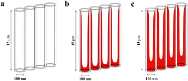
The infiltration of our titania nanotube layers, employing the spin-coating of a chalcogenide glass solution, stems from the procedure used for the filling of nanostructured photonic crystal films described in the literature.33 The basic concept of infiltration of the chalcogenide material inside the titania nanotubes is shown in Fig. 1.
 | ||
| Fig. 1 The concept of infiltrating the titania nanotubes via a tailored spin-coating procedure. (a) Plain tubes, (b) tubes with a low material content (corresponding to 0.1 g As3S7 per ml solution), (c) tubes with high material content (corresponding to 0.166 g As3S7 per ml solution). | ||
The amount of material that is infiltrated can be simply influenced by its concentration in the solution used for spin-coating. As outlined in Fig. 1, the more concentrated the solution, the more material is deposited in the lower part of the tubes. Nevertheless, some material still remains on the tube walls where it forms a thin coating, thus yielding a high surface area sensitizer–nanotube interface. This is advantageous for more efficient light harvesting over the entire tube surface area. The assumption in Fig. 1 is corroborated by photoelectrochemical and EDX analysis as shown below.
Fig. 2a shows an example of the titania nanotube layer, that was used in the present study. All nanotube layers were prepared in the same fashion, by anodization of a Ti substrate for 24 hours in a pre-aged electrolyte containing 0.3 wt% NH4F, ethylene glycol and 2 wt% water, using a two-electrode setup. Afterwards the samples were rinsed with isopropanol and sonicated for 5 minutes to remove the grassy layer on the surface. SEM investigations revealed no remnants of the grass after this procedure, all nanotube surfaces were clean and had open tube mouths. All nanotube layers were annealed, in a muffle oven at 450 °C for 3 hours, to obtain the anatase crystalline phase. The as-prepared nanotube layers were approximately 15 μm thick and consisted of nanotubes with an average outer diameter of 125 nm. In order to always achieve homogenous infiltration of the tubes by the chalcogenide, 1 ml of the prepared As3S7 solution was dropped onto a 1 cm2 area of the tubes which were attached tightly to the Ti substrate underneath. We used a range of concentrations of As3S7 solutions in propylamine34,35 ranging from dilute solutions (0.02 mg ml−1) up to moderate concentrations (0.166 mg ml−1) with high viscosity. It was reported by Kohoutek et al.36 that chalcogenide glass mixtures with amine solvents form nanocolloidal solutions containing 2–8 nm glass clusters over a wide concentration range (comparable with that of our experiment). After spin-coating (2000 rpm) and subsequent vacuum drying at 125 °C for 10 hours,37,38 the as-prepared nanotube layers were subjected to photoelectrochemical measurements.
 | ||
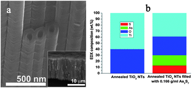
| Fig. 2 (a) SEM image of crystalline TiO2 nanotubes infiltrated with amorphous As3S7 glass, the inset shows the whole tube layer; (b) normalized compositional EDX profiles of TiO2 nanotube layers with and without infiltrated As3S7 (mean values obtained from 20 measurements, standard deviation not exceeding 5% of the given values are displayed). | ||
EDX analyses of the prepared samples confirmed that with increasing As3S7 solution concentration, the nanotube layers became more enriched with As3S7 inside the nanotubes. For comparison, in Fig. 2b we show EDX data obtained from 20 measurements for a plain crystalline titania nanotube layer and the same tubes infiltrated with As3S7 solution at the highest concentration, therefore, with the highest resulting As3S7 content in the nanotubes. A line scan along a cracked piece of tube layer was used so that the values obtained represent the average elemental contents across the whole layer. It is noted that we could not obtain an SEM cross-sectional image of the internal cavity of the infiltrated tubes since the infiltrated tubes do not crack upon mechanical bending of the substrate or cutting with scissors in the way that they do when they are empty. Apparently, they have more mechanical stability due to the presence of the rigid amorphous glass material.
The bandgap energy of pristine spin-coated As3S7 was determined as 2.45 eV (506 nm) using the Tauc formalism and assuming a non-direct optical transition (see ESI, Fig. S1†). In terms of electronic structure, the As3S7 glass – similar to most chalcogenide glasses – is an intrinsic amorphous semiconductor with a low concentration of mobile carriers.39 Its Fermi level can be therefore expected to be positioned in the middle of the bandgap, which is corroborated by its photoelectrochemical behavior, showing a fingerprint typical of intrinsic semiconductors (see ESI, Fig. S2†). A film of pristine As3S7 exhibits very low photocurrents (<1 μA cm−2) and their direction is switched during the potential scan from anodic to cathodic at approximately +0.18 V vs. NHE, coinciding with a Fermi level positioned in the middle of the bandgap.
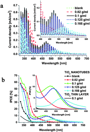
In contrast, after coupling As3S7 to TiO2 by infiltrating the titania nanotubes, a strong sensitizing effect is observed as shown in Fig. 3. The photocurrent response under UV light is enhanced by a factor of two as compared to pristine TiO2 nanotubes for all As3S7 concentrations (Fig. 3a).
 | ||
| Fig. 3 (a) Photocurrent spectra and (b) incident photon-to-electron conversion efficiency recorded for nanotube layers infiltrated with different concentrations of As3S7. The photocurrents were measured at 0.7 V vs. NHE in a Na2SO4 (0.1 M) electrolyte containing KI (0.1 M). For comparison, one typical IPCE curve acquired for a thin TiO2 layer sensitized with the As3S7 0.1 g ml−1 solution is shown. | ||
More importantly, significant photocurrent response can be observed in the visible light range, in particular for medium sensitizer concentrations (0.1 and 0.125 g ml−1), where the highest IPCE (incident photon-to-current efficiency) values, up to 10%, at around 470–480 nm are obtained (Fig. 3b). Given the bandgap of As3S7 (2.45 eV; 506 nm), it is interesting that the visible light-induced photocurrents are detectable even down to 650 nm (1.9 eV), this can be ascribed to the sub-bandgap Urbach tail absorption in As3S7 (see ESI, Fig. S1†). The red shift of the sub-bandgap photocurrent response becomes more pronounced upon increasing the sensitizer content of the nanotubes. This red shift and the presence of maxima in the photo action spectra corroborate strongly our assumption that more material is deposited at the bottom of the tubes as the As3S7 concentration used during spin-coating is increased (Fig. 1).
This can be explained in more detail as follows. Ultimately, the photocurrent generation efficiency at each wavelength will depend on the interplay between three factors: (i) light absorption, (ii) light penetration depth and (iii) the accessibility of electrolyte for the photogenerated holes. Obviously, the effect of the low-energy sub-bandgap absorption of As3S7 (caused by its defect states) on the photocurrent response will be more pronounced with increased amounts of As3S7 in the tubes. This will directly translate into a larger red shift of the photocurrent onset wavelength. On the other hand, since the photoelectrodes are irradiated from the front side (through the electrolyte) and since the light penetration depth increases with increasing wavelength,40 the recombination of photogenerated charges will be enhanced when these are either generated far from the underlying titanium substrate (long distance for electrons to travel), or when they are generated deep in the As3S7 bulk at the bottom of the tubes (long pathway for the holes to travel to reach the electrolyte). Accordingly, depending on the interplay between the irradiation wavelength and the amount of As3S7 at the bottom part of the tubes, a maximum in the photo action spectrum should be observed, with its position moving to longer wavelengths with increasing amounts of sensitizer, exactly as we observed (Fig. 3b). All in all, the medium sensitizer concentrations (0.1 and 0.125 g ml−1) clearly represent the optimum needed for achieving enhanced light absorption in the visible light range without compromising penetration of the nanotube layer by the electrolyte.
It should be noted that the presence of the aligned nanotubular architecture is absolutely crucial for achieving a reasonable sensitizing effect and photocurrent response. Accordingly, negligible photocurrent response in the visible region was observed when a thin crystalline compact TiO2 layer (prepared by annealing a Ti substrate in an oven at 450 °C for 3 hours) was spin-coated with As3S7 (Fig. 3b). Clearly, here the very thin As3S7 layer does not allow for sufficient light absorption, and only the nanostructured assembly is able to achieve efficient light harvesting in the visible light range.
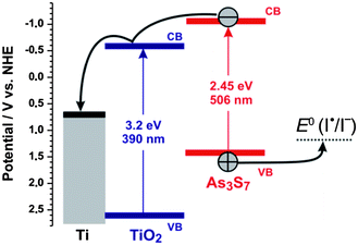
The photocurrent generation under visible light irradiation of a TiO2–As3S7 assembly can be summarized by the potential diagram in Fig. 4. Visible light-induced excitation of As3S7 leads to injection of electrons into the conduction band of TiO2, whereby the holes can oxidize iodide in the solution (E = 1.3 V vs. NHE).41 The presence of iodide in the electrolyte was crucial to achieve long-term stability and avoid photo-corrosion of As3S7, as confirmed by EDX measurements done before and after the photoelectrochemical measurement. It should be noted that this potential scheme is rather simplified. It cannot be ignored that the electron–hole pair in As3S7 is more or less strongly bound (exciton), whereby the quasi-Fermi level of electrons is significantly less negative than the conduction band edge of As3S7. Indeed, the photocurrent onset of the TiO2–As3S7 photoelectrodes was determined to be at ca. −0.4 V vs. NHE and −0.18 V vs. NHE at the wavelengths of 330 nm and 480 nm, respectively (see ESI, Fig. S3†). Interestingly, under visible light irradiation (480 nm) small cathodic photocurrents were observed at negative potentials (the negative Fermi level of the Ti substrate), which suggests that under negative bias the electrons generated in As3S7 can reduce oxygen in the solution, whereby the holes are “neutralized” by electrons injected from the Ti metal through TiO2, presumably via trap states under the conduction band edge.42
 | ||
| Fig. 4 Simplified potential diagram of the TiO2–As3S7 interface at pH 7 under an anodic bias of 0.7 V vs. NHE. The position of the band edges of As3S7 was determined by assuming that the position of the Fermi level was in the middle of the bandgap at 0.18 V vs. NHE; the band edge positions of TiO2 were taken from the literature.43 | ||
It should be noted that, based on our experience, complete filling of the tubes by spin-coating is possible. For our model material, for instance, this can be achieved by using a highly concentrated chalcogenide solution with a high “honey-like” viscosity. This procedure, however, leads to formation of a solid lid on the tube array surface, and therefore has a detrimental effect on the photocurrent due to insufficient contact of the sensitizer with the electrolyte. Quantification of the As3S7 content (or any other sensitizer) inside the nanotubes can be done by EDX, as shown in Fig. 1 and S4.† We will exploit the use of other sensitizers for tube filling in our future work and thoroughly analyze these systems by photoelectrochemistry, EDX and transmission electron microscopy.
Conclusions
We demonstrated that titania nanotube layers can be easily infiltrated with a chalcogenide glass sensitizer by spin-coating with its propylamine solution at an optimized concentration. This technique is low-cost and versatile, and allows the tube walls to be coated, or even for the tubes to be filled entirely, with better control than other approaches, such as electrodeposition, dipping or soaking. The prepared titania nanotubes sensitized with As3S7 have shown significant photocurrent response under visible light irradiation. Taking into account the possibility of tuning the composition of the spin-coating chalcogenide glass solution and/or incorporating other (crystalline) colloidal sensitizers, we believe that the method presented here may pave the way for the fabrication of novel solar energy-converting architectures, photonic devices, p–n junctions or drug-delivery assemblies based on TiO2 nanotubes.Acknowledgements
J.M.M. and T.K. thank project CZ.1.07./2.3.00/20.0254 “ReAdMat – Research Team for Advanced Non-crystalline Materials”, co-financed by the European Social Fund and state budget of the Czech Republic, for financial support. R.B. and L.W. acknowledge financial support from the MIWFT-NRW within the project “Anorganische Nanomaterialien für Anwendungen in der Photokatalyse”. The authors thank Dr Ronald Marschall for a fruitful discussion.Notes and references
- J. M. Macak, H. Tsuchiya, A. Ghicov, K. Yasuda, R. Hahn, S. Bauer and P. Schmuki, Curr. Opin. Solid State Mater. Sci., 2007, 1–2, 3–18 CrossRef PubMed.
- V. Zwilling, M. Aucouturier and E. Darque-Ceretti, Electrochim. Acta, 1999, 35, 921–929 CrossRef.
- R. Beranek, H. Hildebrand and P. Schmuki, Electrochem. Solid-State Lett., 2003, 6, B12–B14 CrossRef CAS PubMed.
- J. M. Macak, H. Tsuchiya, L. Taveira, S. Aldabergerova and P. Schmuki, Angew. Chem., Int. Ed., 2005, 44, 7463–7465 CrossRef CAS PubMed.
- S. P. Albu, A. Ghicov, J. M. Macak and P. Schmuki, Phys. Status Solidi RRL, 2007, 1, R65–R67 CrossRef CAS.
- S. So, K. Lee and P. Schmuki, J. Am. Chem. Soc., 2012, 134, 11316–11318 CrossRef CAS PubMed.
- J. M. Macak, H. Tsuchiya, A. Ghicov and P. Schmuki, Electrochem. Commun., 2005, 7, 1133–1137 CrossRef CAS PubMed.
- K. Zhu, N. R. Neale, A. Miedaner and A. J. Frank, Nano Lett., 2007, 7, 69–74 CrossRef CAS PubMed.
- S. So, K. Lee and P. Schmuki, Chem.–Eur. J., 2013, 19, 2966–2970 CAS.
- J. M. Macak, H. Tsuchiya, L. Taveira, A. Ghicov and P. Schmuki, J. Biomed. Mater. Res., Part A, 2005, 75, 928–933 CrossRef PubMed.
- J. Park, S. Bauer, K. A. Schlegel, F. W. Neukam, K. von der Mark and P. Schmuki, Small, 2009, 5, 666–671 CrossRef CAS PubMed.
- L. Zhao, L. Liu, Z. Wu, Y. Zhang and P. K. Chu, Biomaterials, 2012, 33, 2629–2641 CrossRef CAS PubMed.
- J. M. Macak, M. Zlamal, J. Krysa and P. Schmuki, Small, 2007, 3, 300–304 CrossRef CAS PubMed.
- N. Shreshta, J. M. Macak, F. Schmidt-Stein, R. Hahn, C. T. Mierke, B. Fabry and P. Schmuki, Angew. Chem., Int. Ed., 2009, 48, 969–972 CrossRef PubMed.
- M. Altomare, M. Pozzi, M. Allieta, L. G. Bettini and E. Selli, Appl. Catal., B, 2013, 81–88, 136–137 Search PubMed.
- O. K. Varghese, D. Gong, M. Paulose, K. G. Ong and C. A. Grimes, Sens. Actuators, B, 2003, 93, 338–344 CrossRef CAS.
- B. O'Regan and M. Grätzel, Nature, 1991, 353, 737–739 CrossRef CAS.
- N. Robertson, Angew. Chem., Int. Ed., 2006, 45, 2338–2345 CrossRef CAS PubMed.
- W.-T. Sun, Y. Yu, H.-Y. Pan, X.-F. Gao, Q. Chen and L.-M. Pen, J. Am. Chem. Soc., 2008, 130, 1124–1125 CrossRef CAS PubMed.
- D. R. Baker and P. V. Kamat, Adv. Funct. Mater., 2009, 19, 805–811 CrossRef CAS.
- H. Zhang, X. Quan, S. Chen, H. Yu and N. Ma, Chem. Mater., 2009, 21, 3090–3095 CrossRef CAS.
- K. Shin, S. I. Seok, S. H. Im and J. H. Park, Chem. Commun., 2010, 46, 2385–2387 RSC.
- Q. Shen, K. Katayama, T. Sawada, M. Yamaguchi and T. Toyoda, Jpn. J. Appl. Phys., 2006, 45, 5569–5574 CrossRef CAS.
- F. Wang, Y. Zhang, Y. Liu, Y. Wang, M. Shen, S.-T. Lee and Z. Kang, Nanoscale, 2013, 5, 1831–1835 RSC.
- J. M. Macak, B. G. Gong, M. Hueppe and P. Schmuki, Adv. Mater., 2007, 19, 3027–3031 CrossRef CAS.
- J. M. Macak, C. Zollfrank, B. J. Rodriguez, H. Tsuchiya, M. Alexe, P. Greil and P. Schmuki, Adv. Mater., 2009, 21, 3121–3125 CrossRef CAS.
- D. Kowalski, A. Tighineanu and P. Schmuki, J. Mater. Chem., 2011, 21, 17909–17915 RSC.
- D. Kowalski, S. P. Albu and P. Schmuki, RSC Adv., 2013, 3, 2154–2157 RSC.
- U. Diebold, Surf. Sci. Rep., 2003, 48, 53–229 CrossRef CAS.
- D. Wang, L. Liu, F. Zhang, K. Tao, E. Pippel and K. Domen, Nano Lett., 2011, 11(9), 3649–3655 CrossRef CAS PubMed.
- D. Kim, J. M. Macak, F. Schmidt-Stein and P. Schmuki, Nanotechnology, 2008, 19, 305710 CrossRef PubMed.
- D. Kim, A. Ghicov and P. Schmuki, Electrochem. Commun., 2008, 10(12), 1835–1838 CrossRef CAS PubMed.
- T. Kohoutek, J. Orava, T. Sawada and H. Fudouzi, J. Colloid Interface Sci., 2011, 353, 454–458 CrossRef CAS PubMed.
- G. C. Chern and I. Lauks, J. Appl. Phys., 1982, 53(10), 6979–6982 CrossRef CAS.
- S. Song, J. Dua and C. B. Arnold, Opt. Express, 2010, 18(6), 5472–5480 CrossRef CAS PubMed.
- T. Kohoutek, T. Wagner, M. Frumar, A. Chrissanthopoulos, O. Kostadinova and S. N. Yannopoulos, J. Appl. Phys., 2008, 103(6), 063511–063516 CrossRef.
- T. Kohoutek, T. Wagner, M. Vlcek, M. Vlcek and M. Frumar, J. Non-Cryst. Solids, 2006, 352, 1563–1566 CrossRef CAS PubMed.
- T. Kohoutek, T. Wagner, J. Orava, M. Krbal, T. Mates, A. Fejfar, S. O. Kasap and M. Frumar, J. Non-Cryst. Solids, 2007, 353, 1437–1440 CrossRef CAS PubMed.
- A. V. Kolobov, Photo-Induced Metastability in Amorphous Semiconductors, Wiley-VCH, Weinheim, 2003 Search PubMed.
- J. M. Macak, A. Ghicov, R. Hahn, T. Tsuchiya and P. Schmuki, J. Mater. Res., 2006, 21(11), 2824–2828 CrossRef CAS.
- P. Wardman, J. Phys. Chem. Ref. Data, 1989, 18, 1637–1755 CrossRef CAS.
- T. Berger, D. Monllor-Satoca, M. Jankulovska, T. Lana-Villarreal and R. Gomez, ChemPhysChem, 2012, 13, 2824–2875 CrossRef CAS PubMed.
- R. Beranek, Adv. Phys. Chem., 2011, 786759, DOI:10.1155/2011/7867591.
Footnote |
| † Electronic supplementary information (ESI) available: Details on synthesis of As3S7, photocurrent experiments; electronic absorption spectra and photocurrent measurements of As3S7, potential dependence of photocurrents, EDX analysis. See DOI: 10.1039/c3nr03014h |
| This journal is © The Royal Society of Chemistry 2013 |
