 Open Access Article
 This Open Access Article is licensed under a Creative Commons Attribution-Non Commercial 3.0 Unported Licence
‘Inorganics-in-Organics’: recent developments and outlook for 4G polymer solar cells
K. D. G. Imalka
Jayawardena
,
Lynn J.
Rozanski
,
Chris A.
Mills
,
Michail J.
Beliatis
,
N. Aamina
Nismy
and
S. Ravi P.
Silva
*
Advanced Technology Institute, University of Surrey, Guildford, Surrey GU2 7XH, UK. E-mail: s.silva@surrey.ac.uk
First published on 15th July 2013
Abstract
Recent developments in solution processable single junction polymer solar cells have led to a significant improvement in power conversion efficiencies from ∼5% to beyond 9%. While much of the initial efficiency improvements were driven through judicious design of donor polymers, it is the engineering of device architectures through the incorporation of inorganic nanostructures and better processing that has continued the efficiency gains. Inorganic nano-components such as carbon nanotubes, graphene and its derivatives, metal nanoparticles and metal oxides have played a central role in improving device performance and longevity beyond those achieved by conventional 3G polymer solar cells. The present work aims to summarise the diverse roles played by the nanosystems and features in state of the art next generation (4G) polymer solar cells. The challenges associated with the engineering of such devices for future deployment are also discussed.
1 Introduction
Social and ethical responsibility for sustainable growth while not damaging the eco-system we live in is persuading nations increasingly to examine renewable sources for powering society. Growing concern over the diminishing fossil fuel supplies, as well as other considerations such as the impact of fossil fuel based energy generation on global warming and climate change, has led to intense research into renewable energy generation. Of the myriad routes available for the conversion of solar energy to electrical energy, photovoltaics (PVs) are fast becoming a viable route towards energy generation. This is both from a mobile, remote, off grid small scale energy source to large scale grid-connected solar energy farming.Over the years, several techniques have been investigated for the conversion of light into electrical energy, with the use of semiconductors that absorb light in the visible region being the most successful. Semiconductors are materials that generate free carriers (in inorganics such as Si and GaAs) or excitons (in organics, which are dissociated to form free carriers) when exposed to photons with energies exceeding their optical bandgaps1 (single walled carbon nanotubes are inorganics known to be an exception to the above rule, as they generate excitons upon photoexcitation due to their one dimensional nature). These charges, once separated are swept through the device via a built in field and extracted at the contacts, which can be used to drive a load and provide useful power output.
Over the years, the development of PV technology has undergone numerous changes leading to the cells being classified2 into different generations, originally defined for inorganic materials as high cost/high efficiency (1st generation), low cost/low efficiency (2nd generation) and low cost/high efficiency (3rd generation). Traditionally, the 1st generation (1G) PV technology is known to comprise of photovoltaic technology based on thick crystalline films (mainly Si) which not only leads to high efficiency, but also high cost. The 2nd generation (2G) of solar cells was developed with the aim of reducing the high costs prevalent in 1G through the utilisation of thin film technology. The idea was to save on bulk material cost with a significant reduction in the quality and quantity of the material used, with the challenge of increasing the thin film absorption to compensate for the reduced thickness in the photoactive layers. This 2G thin film technology was based on PV materials identified during the development of 1G PVs and was extended to include amorphous or polycrystalline Si, CIGS, and CdTe. While the 2G PV family addresses the cost issues associated with thick films, the performance of such 2G solar cells is known to be poor compared to their 1G counterparts. Therefore, the challenge was to improve the efficiency as much as possible within the inexpensive material envelope that encouraged the chemical vapour deposition of thin films and thermal crystallisation, where appropriate. In the case of amorphous materials, to compensate for the significantly reduced active volume, an intrinsic layer was grown to produce p–i–n devices where photogenerated carriers could be swept to the doped materials by the built-in field. The key factor that worked in favour for 2G PV cells was the $/W, cost per watt, delivery, but the need for extended surface areas to compensate for the lower efficiency was an issue.
This in turn pushed the development of 3rd generation (3G) solar cells, including nanocrystalline films, PVs based on active quantum dots, tandem or stacked multilayers of inorganics based on III–V materials such as GaAs/Ge/GaInP2, or novel device concepts such as hot carrier cells2 where the aim was to obtain higher performance than their 2G counterparts, at lower cost. A true race to design materials at the nanoscale and scale-up to the macroscopic areas was ignited. For the first time significant attention was paid to charge and energy transfer processes, and routes to optimise charge collection and enhance the energy capture within the solar spectrum. With the introduction of organic materials exhibiting photovoltaic properties, their potential for low cost and high optical absorption placed them as a 3G technology. In addition to organic (or polymer) solar cells, another candidate that grew to dominate 3G PV technologies is dye or semiconductor sensitised (or mesoscopic) solar cells (DSSC). Despite the reasonable success of 3G cells, significant improvements in device performances are required if this technology is to be competitive with the previous PV generations in terms of cost per watt.
As such, the 4th generation (4G) of PV technology was introduced, which combines the low cost/flexibility of polymer thin films with the stability of novel inorganic nanostructures with the aim of improving the optoelectronic properties of the low cost thin film PVs. These device architectures are meant to maintain the inexpensive nature of a solution processable PV device structure; but incorporate inorganic components to improve on energy harvesting cross-sections, the charge dissociation, and charge transport within the PV cells. While the previously introduced mesoscopic solar cells may be considered as a 4G technology due to the incorporation of an inorganic component (usually titania), especially when combined with a polymer or organic layer as a solid-state DSSC, we note that this inorganic component is a requirement for the functionality of the cell and does not introduce additional benefits as for the inorganics-in-organics architectures discussed here. Therefore, we believe such mesoscopic cells are better classified as a 3G technology. An illustration of the different generations is shown in Fig. 1.
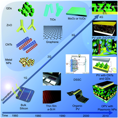 | ||
| Fig. 1 Timeline of the four generations of photovoltaic devices, illustrating the changes from first generation (1G) to fourth generation (4G) with associated nanomaterial components that comprise half of the 4G devices. | ||
To date, the most effective polymer solar cells (PSCs) have been based on the bulk heterojunction (BHJ) concept first proposed by Yu et al.3 This involves combining both the donor (D) and the acceptor (A) into a single composite layer where spontaneous phase separation occurs between the exciton generating polymer and a fullerene derivative [6,6]-phenyl C61 butyric acid methyl ester (PC61BM) or [6,6]-phenyl C71 butyric acid methyl ester (PC71BM) that assist in the dissociation of the photogenerated excitons through the formation of localised nanoheterojunctions.4,5 For efficient exciton dissociation in the nanoheterojunction between these phases, the exciton should be formed within the exciton dissociation length (∼10 nm) within the D phase.4,5 Furthermore, the phase separation should proceed such that each phase forms a percolation pathway or connectivity to the respective electrodes such that charges are extracted with minimum recombination (Fig. 2a)).6 For this to occur, the charge transfer, with its subsequent exciton separation must take place before recombination occurs.
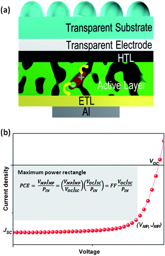 | ||
| Fig. 2 (a) The bulk heterojunction architecture, now widely used for fabricating high performing polymer solar cells. The excitons are (mainly) formed within the D polymer. Dissociation of these excitons occurs at the D:A interface leading to hole transport through the D and electron transport through the A. (b) Current density–voltage characteristics of solar cells showing the open circuit voltage (VOC), short circuit current density (JSC) and the maximum power point with a voltage and current density of VMP and JMP respectively. The equations relating the above parameters to PCE are also given. | ||
Initial research on PSCs was based on polyphenylene vinylene derivatives (PPV)3,7 followed by regioregular poly(3-hexylthiophene) (rr-P3HT); the “fruit fly” of PSC research.8,9 Due to the relatively large bandgap of such materials,10 the power conversion efficiency (PCE) remained well below the 10% level desired for laboratory scale devices required before large scale deployment of the technology. However, an ever increasing knowledge of engineering of polymers has led to the development of new low bandgap polymers which are now showing significant promise, with PCEs exceeding 7%.11–13 Despite such innovations in the synthesis and design of polymer semiconductors, the PSC performances remain limited by two factors: (1) the PSC active layers are known to possess relatively low charge mobilities, which necessitate thin films, resulting in (2) low optical absorption, leading to suboptimal current generation. For example, BHJ PSCs based on rr-P3HT are known to produce current densities of ∼10 to 11 mA cm−2 under short circuit conditions,9 which is below the 15 mA cm−2 (ref. 14) maximum achievable for a polymer solar cell with an equivalent bandgap. Therefore, in order to realize the full potential of such material systems, methods to enhance charge transport within the active layer as well as improved optical coupling are desired. In terms of device performance characteristics, this correlates with the enhancement of device performance parameters such as the short circuit current density (JSC) and the fill factor (FF) (Fig. 2(b)).
The concept of 4th generation (4G) solar cells has been developed with the aim of realising both improved charge transport15 and an improvement in the optical coupling,16 in PSCs through the incorporation of inorganic nanostructures into the device architecture. In addition to the optical and electronic benefits of incorporation of inorganic systems within active materials, certain inorganic materials are also known to improve the device lifetime as well.12 Although a number of review articles on the optical and electrical enhancements due to inorganics-in-organics have been published over the years, most of them have focused on specific inorganic materials [such as carbon nanotubes (CNTs) or metal nanoparticles (mNPs)].17–20 In this review article, we holistically examine the role of inorganic nanomaterials in the different parts of the PSC device architecture, including electrodes, active layers and interfacial layers, illustrated in Fig. 3. We show that the inorganic component enhances optical coupling and/or charge extraction, as well as device lifetimes which radically modify the manner in which modern PSC devices are engineered. As such the focus is on the use of materials such as CNTs, graphene, mNPs, and metal oxides, as well as nanohybrid materials, used in different layers of the PSC device architecture.
 | ||
| Fig. 3 “Inorganics-in-organics”. The utilisation of inorganic nanostructures in the different layers of PSCs. | ||
Within this review, an introduction is given to the different inorganic systems now widely used in 4G solar cells. This is followed by a discussion of alternative technologies available to replace the widely used transparent tin doped indium oxide (ITO) contact. We focus on alternatives such as CNTs, graphene, metal nanowires and metal grid structures that can be either printed or stamped in line with the requirements for roll-to-roll processes. This is followed by a section on interfacial layers based on inorganic systems such as CNTs, metal oxides, graphene and its derivatives, as well as carbon–metal oxide nanohybrids. In addition to the functional aspects of such materials, these also provide a route towards more stable, long life devices, paving the way for manufacturable products. This review article also discusses the utilisation of inorganics within the active “nano-hybrid” layer, where nanostructures such as CNTs are used as efficient charge transport pathways and metal nanoparticles are used to improve exciton dissociation and light scattering sites. Finally we conclude by identifying areas for future improvement of such 4G PSCs that will enable a revolution in cheap affordable renewable energy sources, where society can take responsibility for its own carbon footprint.
2 Inorganics-in-organics
The widely used inorganic nanostructures in PSCs can be classified into 3 groups: carbon nanostructures, metal nanoparticles and metal oxides. In this review, we have intentionally chosen to forgo a discussion on quantum dots.CNTs, first reported in the scientific literature by Sumio Iijima,21 are tubules of graphene with unique electronic and optical properties. Depending on the number of coaxial tubes present, CNTs are classified (structurally) as single walled, double walled or multiwalled.22 The properties of an individual CNT are strongly dependent on the wrapping configuration (or chirality) (Fig. 4) of the tube. As such, single walled carbon nanotubes (SWNTs) can be further classified as being metallic or low bandgap semiconductors. Multiwalled carbon nanotubes (MWNTs), on the other hand, are metallic in nature due to the range of chiralities present. While the properties of MWNTs appear more or less clearly defined, SWNTs show more complexity due to the difficulty in controlling chirality during growth. However, recent developments in growth (e.g.: cobalt molybdenum catalyst (CoMoCAT) growth technique) and non-covalent functionalization techniques23,24 have allowed nanotubes with specific properties of chiralities to be isolated.25 Due to the broad nature of chirality control and functionalization techniques, readers are encouraged to refer to the literature25,26 for more in-depth discussions.
 | ||
| Fig. 4 Schematic of SWNTs with (a) arm chair, (b) zigzag and (c) general (often referred to as chiral).22 The electronic and optical properties of such nanotubes are dependent on the chirality of the nanotubes. The alignment of the carbon–carbon bonds with respect to the tube axis are highlighted in red for (a) and (b). The images are generated using the Ninithi freeware, v1.0 (http://ninithi.lk/). | ||
One of the important properties of carbon nanotubes, be it single walled or multiwalled, is the unique charge property that results in ballistic transport.22 However, charge transport in CNT networks are often impaired by junctions27 that leads to mobilities less than 1 cm2 V−1 s−1. The mobilities achievable by CNTs remain sufficient in view of the very low hole (electron) mobilities in PSC active layers, which usually are less than 10−3 cm2 V−1 s−1.28
In addition to CNTs, graphene, another carbon allotrope is now beginning to attract significant attention for organic electronic devices. First isolated through the now famous scotch tape method,29 graphene is a 2D system consisting of carbon atoms arranged in a hexagonal structure through sp2 bonding. Among the principal attractions of graphene for its utilisation in organic electronic devices are its high carrier mobility of ∼2.6 × 105 cm2 V−1 s−1 (ref. 30) and optical transmission approaching 97% at 550 nm.31 However, such electric properties have only been reported for micromechanically cleaved graphene samples, while the conduction properties of large area graphene produced through chemical vapour deposition has led to poorer charge transport properties.31,32 Another disadvantage of chemical vapour deposited graphene has been the requirement for etching of Cu foil used for graphene growth and the subsequent transfer techniques. The latter results in organic residues33 on the graphene sheet significantly affecting its transport properties.32 As a result, recent attempts for graphene synthesis have also focused on preparation of graphene solutions34 that can be printed35 or deposited on substrates using methods compatible with roll-to-roll processes.
Wide band gap metal oxides are another class of the material system that has recently attracted significant attention for organic electronics. While their wide bandgap nature36 makes them less favourable as an optically active component in most organic optoelectronic devices, metal oxides such as titanium oxide (TiO2 or TiOx), zinc oxide (ZnO) and molybdenum oxide (MoO3) have found use as interfacial layers.9,12,16 Not only do the Fermi levels of these materials allow favourable electron or hole extraction, but they are also known to be effective moisture and oxygen scavengers37 that results in prolonged lifetimes for organic electronic devices.
Metal nanostructures form the third class of materials discussed in this review. While there exists a range of metals that can be utilised in organic electronic devices, gold (Au) and silver (Ag) have been widely investigated due to the possibility of improving organic optoelectronic device performances through plasmonic effects17 as well as the capability of forming a new generation of transparent conductors for optoelectronic devices.38
3 Inorganic transparent electrodes
Typically, a solar cell consists of the solar radiation-absorbing active materials and charge transport layers sandwiched between two electrodes: a transparent conducting electrode (TCE), which allows the incident solar radiation to enter the cell; and a non-transparent, usually metallic, rear electrode, which has the dual function of the electrode and the reflector material to reflect the light back into the active material.ITO is currently the preferred TCE for solar cell construction. With a sheet resistance as low as 10 Ω □−1 and high visible light transmission (an average of 85% transmission from 400–700 nm), ITO has been widely utilised, and its fabrication process has been thoroughly optimised.39 However, its limitations, including reduced conductivity on bending,39 scarcity of indium,40 high processing temperatures, and potential indium migration,41,42 have prompted researchers to look for alternatives, in particular with the development of flexible organic electronics.43
At the other extreme of the device, the metallic rear electrode has typically been produced from atmospherically-stable metals such as aluminium (Al) or gold (Au), by thin layer evaporation techniques. Other electrode structures incorporating lithium fluoride (LiF), magnesium (Mg) or calcium (Ca) are available, encapsulated with a layer of the aforementioned atmospherically-stable metals.44 The material chosen for the rear electrode is based on the energy levels in the active/transport materials and the front TCE so that the electrode produces an Ohmic contact. Again, researchers have been looking to minimise, or replace, the metals used in the construction of solar cells, given the high cost of some metals, and the potential for diffusive metal ion poisoning of active layers.
Novel technologies considered for the production of next generation TCE materials include the use of non-indium containing oxides,45 thin metal films (a few nanometres thick to retain transparency),46 metal grids,47 or nanomaterials, such as CNTs,48 graphene,49 or silver nanowires50 (Fig. 5). These technologies can be compared by examining their performance with respect to optical transparency and electrical sheet resistance.
 | ||
| Fig. 5 Examples for (a) large area spray coated transparent carbon nanotube electrodes (reproduced with permission from ref. 51, Copyright 2009, Wiley), (b) transparent graphene electrodes on a flexible substrate (reproduced with permission from ref. 52, Copyright 2010, American Chemical Society), (c) silver nanowire networks (reproduced with permission from ref. 50, Copyright 2009, American Chemical Society) and (d) transparent metal grids (reproduced with permission from ref. 53, Copyright 2013, Optical Society of America). | ||
Transparent conducting electrodes at present are typically based on impurity-doped zinc-, indium- or tin-oxides (ZnO, In2O3 and SnO2) or multicomponent oxides consisting of a combination of these three compounds.45 Of these, ITO is the most commonly used. Other possible transparent conductors such as aluminium- and gallium-doped ZnO (AZO and GZO) semiconductors, with source materials that are inexpensive and non-toxic are also being researched. In particular, AZO thin films meet this requirement, along with a low resistivity of the order of 5–10 Ω cm.
Whilst it is possible to produce semi-transparent thin metal films with thicknesses less than 50 nm, there tends to be a trade-off between sheet resistance and light transmission. Sheet resistance requires the homogeneous area coverage provided by a thicker metal film, but transmission falls off dramatically as the film thickness increases.46 Discontinuous metal films, or metallic grids, offer a solution to this problem as the inter-grid gaps allow for transparency, but the grid lines can retain their thickness and hence conductivity.54 They may also be deposited using a range of microengineering techniques, such as thermal imprint, flexographic, inkjet, and roll-to-roll processes.47
Low sheet resistances are possible with silver nanowires,50 and the contact resistances between individual nanowires can be reduced by sintering.55 Solution processable silver nanowire electrodes have been produced that, when planarised (5 nm roughness) with a layer of the conducting polymer, give a sheet resistance of 11 Ω □−1 and a transparency of 87%.56 Carbon nanomaterials, such as CNTs, have relatively high charge carrier mobilities57 and can display ballistic conduction at room temperature.58 They have a low percolation threshold, so in theory only a low concentration would be required to achieve a low sheet resistance suitable for TCEs. The low concentrations needed would imply that the light absorption of the resultant TCE would also be low. Unfortunately, the contact resistance between individual nanotubes is very high, and to achieve a sheet resistance of 10 Ω □−1, CNT films alone need to be more than 100 nm thick.39 Even so, CNT films have been used with a reported sheet resistance of 30 Ω □−1 and an average transmission of 70% throughout the visible wavelength range (400–700 nm).46 The surface roughness of a film of nanotubes, which is related to the diameter of the nanowires, can also be on the order of 100 nm. This is relatively large and can short circuit most thin films used in optoelectronic devices. The nanowires are also heterogeneously arranged, and local sheet resistance or transmission can be worse than the calculated average values. Graphene is potentially the ultimate TCE, being a light-weight, conducting, single layer of sp2-bonded carbon atoms arranged in a hexagonal grid (honeycomb) structure. Graphene has a measured sheet resistance on the order of 300 Ω □−1,59 and a transparency of more than 97% at 550 nm, and greater than 95% from 400–1000 nm.60 Although it is possible to produce graphene over large areas,60 typically graphene is actually prepared in “few-layer” graphene (FLG) sheets, where overlapping micrometre sized graphene flakes are deposited on a surface. Unfortunately, as for the conduction between individual nanowires, the grain boundaries formed in FLG present a barrier to charge conduction, increasing the sheet resistance.61 However, modern micro fabrication techniques, using roll-to-roll printing (Fig. 6) techniques, have made it possible to produce single graphene sheets over a large area without defects or structural kinks that increases conductivity.60 As such, graphene represents an excellent candidate for the future production of large area TCEs. However, it should be noted that in order to reach the 15 Ω □−1 sheet resistance desired for the transparent conductor, ∼20 mono-layers of graphene require to be stacked which in turn can lead to a significant drop in light transmission which in certain cases can be as high as 50% (Fig. 7).
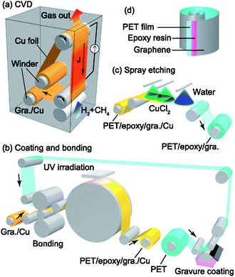 | ||
| Fig. 6 Schematic of continuous roll-to-roll CVD growth and transfer of large area graphene (reproduced with permission from ref. 62, Copyright 2013, American Institute of Physics). | ||
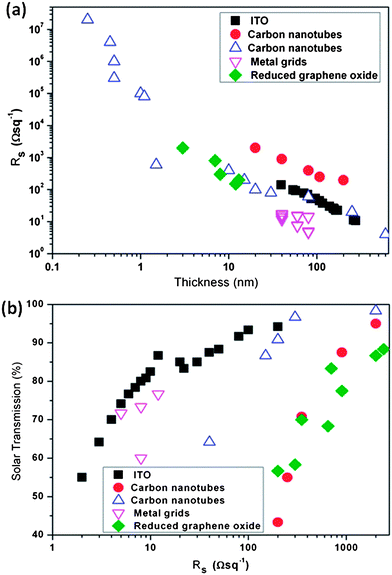 | ||
| Fig. 7 (a) Dependence of sheet resistance on film thickness and (b) dependence of solar transmission over the whole spectrum on the sheet resistance for ITO,66 CNTs,67–69 metal grids70 and reduced graphene oxide electrodes.60 | ||
To overcome the problem of conduction between individual elements of the carbon nanomaterial, researchers have looked at adding functionality to the surface of the carbon which can act as a conducting bridge. It is possible to chemically functionalise the carbon nanomaterial directly49 or introduce conducting co-polymers through physical interactions.24 The functionalization assists in overcoming conduction barriers at grain boundaries and between nanowires.
The use of nanomaterials also allows for the large volumes surrounding the nanomaterial to be filled using a conducting medium, such as a polymer49 or other nanomaterials.63 In general, this means that the active materials or transport layers of the solar cell penetrates the electrode matrix, enabling conduction interactions over a larger surface area than would be the case with a solid electrode layer. For example, a poly(3,4-ethylenedioxythiophene) poly(styrenesulfonate) (PEDOT:PSS) layer coated on a CNT or graphene electrode will fill the space between the carbon materials, to improve conductivity, and acts as an energy level step from the electrode to the active materials. A composite graphene/CNT electrode is shown to have a series resistance of 636 Ω □−1 and transmission of 92%; better performance than the individual component TCEs.63 For a TCE, the highly conducting nanomaterial can be used in a low concentration within a transparent conducting host matrix, increasing transparency without sacrificing conductivity.
It may be that one of these novel electrode technologies alone will not satisfy the requirements for high optical transparency and low sheet resistance required for next generation solar cell technology, and it may be that a combination of technologies is required. For example, metallic grids suffer from a lack of conduction between the lines of the grid. On the other hand, it is difficult to produce a defect free graphene monolayer over large areas. The combination of FLG over which a metallic grid is evaporated combines the advantages of graphene's transparency with the excellent conductivity over large areas of the metal grid. The FLG ensures good transparency in the areas between the metal grid lines, while the metal grid provides the long range conductivity that FLG lacks.
Finally, the electrode architecture is not limited to the conventional transparent front electrode/reflecting rear electrode configuration. Progress in the solar cell design has also lead to the development of cell architecture, with back-junction (BJ), emitter wrap-through (EWT) and metallisation wrap-through (MWT) electrodes as novel electrode configurations for back-contacted solar cells with reduced resistivity losses.64 With PSCs looking to increase in size, such electrode architectures may find use in existing flexible, ultra-thin, light-weight PSC cells.65
4 Inorganics for transport layers
Hole transport layers
The most common commercially available material used as a hole transport layer (HTL) in organic electronics is PEDOT:PSS,71 which acts to smooth the underlying transparent electrode (or planarise), as well as to facilitate the injection of holes into the active layer. However, devices made with PEDOT:PSS suffer from reduced device lifetimes due to the highly-acidic and hygroscopic nature of the polymer mixture,72,73 which has initiated the search for an air-stable, highly transparent and effective replacement hole transport material. Initial tests into novel hole transport materials include using evaporated thin films of transition metal oxides (TMO) such as tungsten oxide (WO3), vanadium oxide (V2O5), MoO3, and nickel oxide (NiO), which have the advantage of air stability, excellent transparency across the visible region and can be easily be applied to both conventional and inverted device structures.74–77 These particular TMOs have an advantage for use as hole transport layers due to their relatively high work functions (ranging from 5.3 eV for NiO to 6.7 eV for MoO3), allowing the user to selectively match the energy barrier level to the donor polymer for enhanced hole extraction.78 Furthermore, these metal oxides form an excellent Ohmic contact with either the ITO anode, or the metallic back cathode, facilitating charge extraction.One setback for using these metal oxides is that they often require high temperatures and vacuum for evaporation. As a result, various groups have designed different methods for forming high quality TMO layers through solution processing, such as spincasting, printing, or spraying. There are two solution-based methods for making TMO films: either using colloidal dispersions of TMO nanoparticles grown separately, then spincast onto a film, or ‘growing’ TMO nanoparticles from a precursor film spun onto the substrate through annealing. The three most commonly used TMOs, MoO3, V2O5, and NiO, have all been investigated using these methods. Early dispersions of MoO3 required the addition of polymer buffers to prevent agglomeration, which then required plasma treatment to remove, hindering the ability to be used in inverted PSC.79 Films made from dispersions of both MoO3 and V2O5 nanoparticles suffered from poor film quality with large surface roughness and incomplete surface coverage.80,81 The second method is better, with nanoparticles grown from sol–gel films producing quality thin films with results matching their evaporated counterparts.82–85 Some problems remain with the sol–gel methodology, with some MoO3 films requiring temperatures up to 250 °C, while some of the V2O5 films require long treatment times.82,86 To overcome these challenges, some groups have implemented low-temperature synthesis approaches, with annealing temperatures at a PSC-compatible range of 70–100 °C.87,88 This has resulted in both a lifetime and efficiency enhancements for the PSCs incorporating these materials.
Some metals, such as gold, have work functions that are very efficient for hole injection. However, just a few scant nanometers of the gold film will completely block light transmission into the device, and therefore the interest is on using mNPs, which can allow for additional light absorption via localized surface plasmon resonance (LSPR) effects.89 Using mNPs which are smaller than the wavelength of light entering a device, can increase the amount of light absorbed by the solar cell.90,91 Similar to TMOs, mNPs can be formed through a variety of methods including chemical synthesis,92 thermal annealing,93 E-beam lithography,90 and laser annealing.94 Solution-processed mNPs have the same dispersion and film quality limitations as observed for similarly prepared TMOs, while the thermal methodology used requires high temperatures and vacuum processing which adds costs and complexity. Lithographic techniques nominally do not translate to large areas, and therefore much interest has been raised in using lasers for NP formation. Care needs to be associated with the incorporation of mNPs, as they can electrically short the device. However, when mNPs are included into the HTL of organic solar cells (either underneath a polymer hole-transport layer, or as part of the same layer), an enhancement primarily in current density is observed resulting in higher efficiency.
In addition to the aforementioned materials, considerable research has been expended into carbon-based allotropes, which have excellent energy-level matching for injecting holes and are environmentally-friendly materials. These materials have high thermal, oxidative and chemical stability, making them a good alternative to the traditional PEDOT:PSS hole transport layers. CNTs have been well-studied as potential interfacial layers for this same reason, and they also have been investigated for TCEs. Due to the ability to functionalise carbons with a plethora of moieties, the work function and affinities can be tuned for either electron or hole transport/injection. As prepared CNTs tend to aggregate in bundles, and do not easily disperse unless they are treated with a surfactant95 (decreasing film conductivity), or functionalized with soluble small molecules or polymers through covalent96 and non-covalent techniques.24,97 These functionalization methods are more common, as they facilitate smooth, well-dispersed CNT films, without inhibiting conductivity. Covalent functionalization occurs through chemical modification of the CNT sidewall, either through acid treatments that introduce hydroxyl and carboxyl groups, or through the attachment of small molecule or polymer chains directly. Covalent functionalization, while creating water soluble CNTs, damages the nanotube sidewalls, which can decrease conductivity in the final film. Non-covalent functionalization, where small molecules or polymers adhere to the sidewall through van der Waals force π–π stacking, leaves the CNT undamaged while still soluble in common solvents. Using non-covalent functionalization with the polymer rr-P3HT on SWNTs, a thin film with transparency equivalent to PEDOT:PSS produces PSC with a higher fill factor and efficiency over the PEDOT:PSS reference (Fig. 8).98
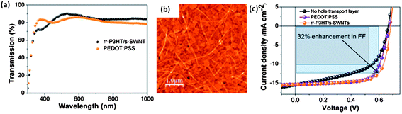 | ||
| Fig. 8 (a) Optical transmission, (b) atomic force micrographs and (c) J–V characteristics of rr-P3HT/s-SWNT nanohybirds as hole extraction layers (reproduced with permission from ref. 24, Copyright 2013, American Chemical Society). A higher optical transmission is obtained for these nanohybrids compared to PEDOT:PSS, together with an improved device performance compared to PEDOT:PSS HTL based devices. | ||
Similar to CNTs, graphene is another material system that has primarily been used as a hole transport layer in its oxidised form. When oxidised, graphene (or graphene oxide (GO)) is known to be water-soluble, with a lower work function compared to pristine graphene, making it better for hole injection. The most common route to make GO is through the Hummer's method, where inexpensive graphite powder is oxidized using a mixture of sulphuric acid, sodium nitrate and potassium permanganate, from which individual or few-layer flakes of oxidized graphene are exfoliated via sonication.99 Similar to covalent functionalization of CNTs, this oxidation process disrupts the conductivity of graphene, making it more insulating. However, the GO has been used as an effective, stable replacement for PEDOT:PSS in solar cells because it has a higher conductivity in the vertical direction which allows for tunnelling between planar overlapping sheets.100 Partial-reduction of GO, to enhance conductivity in both the vertical and lateral directions, has also produced devices with efficiencies that matched that of the PEDOT:PSS reference.101
Electron transport layers
There are not as many electron transporting materials as there are hole transporting materials, and some of the most commonly used materials are highly reactive alkali earth metals such as calcium or magnesium (with low work functions), or lithium fluoride, which facilitates electron tunnelling into a film. These materials need to be evaporated, requiring high vacuum and melting of metals to high temperatures for deposition. Shifting to solution-processable nanomaterials such as CNTs or TMOs will facilitate the transfer of full device fabrication to roll-to-roll processes. One of the advantage of the carbon-based nanomaterials is the ability to tune their energy levels through chemical modification, allowing them to function for electron injection instead of hole injection. Multi-walled CNTs have had their outer walls doped using thermal treatments with an ammonia/argon gas etch to introduce nitrogen ions into the wall, lowering their work function from 4.6 eV for the pristine nanotubes to 4.4 eV (conversely, boron is also added to make CNTs more p-type).102 This lowered work function makes them suitable for electron injection into a device, and unlike the more common electron transport materials, do not degrade with exposure to water or oxygen. In a similar fashion, GO can have its acid –COOH groups esterified to –COOC groups through charge neutralization,103 lowering GO's work function from 4.7 eV to 4.0 eV. This neutralization was performed by mixing GO with Cs2CO3 in water, producing highly transparent films which could be used in an inverted device structure. Furthermore, devices made using the neutralized GO layer performed better than their reference, Cs2CO3 alone, resulting in a device that used the same base material (GO) for both hole and electron transport layers.103Similar to the TMOs used for hole injection, the TMOs used for electron injection have high electron mobilities, high transparency as films, and are air-stable. There are not many n-type TMOs that can be used, with the most popular for electron injection being TiOx or TiO2, ZnO and AZO. For these TMOs, the focus has been on solution-processed films, often through thin, highly transparent layers grown through a sol–gel process. TiOx, used as both an electron transport layer and an optical spacer (to shift the light intensity maximum within the active layer), produced PSC with nearly 100% internal quantum efficiencies.104 As a sol–gel, the diluted precursor solution was spincast, then annealed at 80 °C to form an amorphous layer of TiOx. The sol–gel process has also been used for ZnO,105 producing well controlled NP sizes and smooth films, and additionally, when used in the inverted device structure, the ZnO can absorb damaging UV rays to extend device lifetime. TiO2 and ZnO nanoparticles have been synthesized in solution, prior to diluting them down for application to the PSC.106 While these nanoparticles have varied sizes which can be larger than the sol–gel method, leading to higher film roughness, this does not require an additional heating or sintering step. Doping of ZnO nanoparticles with aluminium, to form AZO, has produced more conductive thicker ETL layers, commercially favourable for roll-to-roll printing in addition to protecting the underlying layers.107 Unfortunately AZO, requires high annealing temperatures (200–260 °C) that are unfavourable for flexible plastic substrates or many of the latest PSC active layers.
Of interest recently has been combining the advantages of both TMOs and carbon nanoparticles. The ability to tune the GO's work function allows it to facilitate electron injection when combined with a TMO as a double electron-transport layer, where the tuned 4.3 eV of GO facilitates charge extraction through a tiered stepping to the electrode.108 This double electron transport layer produced higher efficiency (7.50% versus 7.02%), mainly through an enhanced fill factor, due to the reduced series resistance of the tiered steps. Similarly, a thin layer of TiOx deposited by atomic layer deposition onto a network of CNTs facilitates blocking holes through the CNTs, and allowing electron transport while retaining the high flexibility and transparency of the CNTs.109
Incorporation of metallic nanoparticles to the interlayer
In addition to electronically engineering the active layer/contact interface for favourable charge extraction, another role of interfacial layers is the improvement of light coupling into the active layer. In this regard, inclusion of mNPs that can preferably scatter light into or within the active layer is an area of extreme interest. Due to exciton quenching effects by mNPs in the active layer, certain groups have preferred the incorporation of mNPs into the interfacial layer of PSCs. This has generally involved the introduction of mNPs coated with surfactants into PEDOT:PSS; the widely used solution processable hole transport layer in polymer solar cells. Initial investigations in this area focused on the incorporation of Au or Ag mNPs in combination with an active layer of rr-P3HT:PC61BM which led to improvements in PCEs ranging from 20–70% (ref. 110–113) or together with poly[2-methoxy-5-(2′-ethylhexyloxy)-p-phenylene vinylene] (MEH-PPV) which led to an enhancement in PCE of ∼19%.114 Recently, Lu et al.115 have reported the impact of mNPs in PEDOT:PSS with poly[[4,8-bis[(2-ethylhexyl)oxy]benzo[1,2-b:4,5-b′]dithiophene-2,6-diyl][3-fluoro-2-[(2-ethylhexyl)carbonyl]thieno[3,4-b]thiophenediyl]] (PTB7):PC71BM active layers. While the incorporation of Ag or Au nanoparticles with diameters in the range of 40–50 nm led to an improvement in the device performance from 7.25% to 8.01% and 8.16% (respectively), incorporation of both Ag and Au mNPs into PEDOT:PSS was observed to result in a PCE of 8.67%, the highest reported so far for 4G PVs with mNPs. Work reported along similar lines by Baek et al.116 where Ag nanoparticles were incorporated into PEDOT:PSS has also revealed a significant improvement in PCEs from 6.4% to 7.6% for poly[[9-(1-octylnonyl)-9H-carbazole-2,7-diyl]-2,5-thiophenediyl-2,1,3-benzothiadiazole-4,7-diyl-2,5-thiophenediyl] (PCDTBT):PC71BM and from 7.9% to 8.6% for PTB7:PC71BM indicated the importance of such plasmonic nanostructures. One of the more recent investigations that again suggests the possibility of improvement of polymer solar cells through plasmonic effects has been the incorporation of both mNPs in the active layer and a backgrated electrode for dual plasmonic effects in poly{[4,8-bis-(2-ethyl-hexyl-thiophene-5-yl)-benzo[1,2-b:4,5-b′]dithiophene-2,6-diyl]-alt-[2-(2′-ethyl-hexanoyl)-thieno[3,4-b]thiophen-4,6-diyl]} (PBDTTT-C-T):PC71BM inverted 4G solar cells (Fig. 9).117 While the incorporation of a backgrating or mNPs (20 or 50 nm in diameter) on its own leads to PCEs of 8.38%, 7.83% and 8.11%, the dual plasmonic structures yield PCEs of 8.79% in comparison to flat 3rd generation reference devices with a PCE of 7.59%.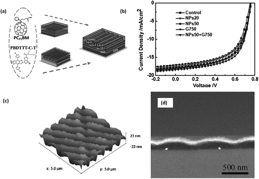 | ||
| Fig. 9 (a) Schematic of dual plasmonic architecture reported in ref. 117, (b) the relevant J–V characteristics for backgrated (only) devices, 20 nm diameter and 50 nm diameter Ag nanoparticles and the dual plasmonic structures, (c) atomic force micrograph of 750 nm pitch backgrating and (d) cross sectional SEM images indicating the positioning of Ag nanoparticles within the active layer. The profile of the backgrating can also be observed (reproduced with permission from ref. 117, Copyright 2012, Wiley). | ||
In addition to their use in interlayers for single junction devices, mNPs have also been incorporated into interconnecting layers in multijunction or tandem solar cells.118 For example, Au mNPs with a diameter of ∼70 nm were incorporated in the interconnecting layer between rr-P3HT:indene-C61 bisadduct (IC61BA) and PSBTBT:PC71BM which led to an improvement in the PCE from 5.22% to 6.24%. However, this remains one of the few reports on improvement in light coupling to multijunction organic solar cells.
5 Inorganics in organic active layers
Modern organic photovoltaic device architecture, first introduced by Yu et al.,3 is based on blends of exciton generating semiconducting polymers and fullerene derivatives. The competing effect between effective optical coupling into the active layer and the poor charge transport properties in the D and A system has led to 80–100 nm as being the preferred thickness regime for optimum exciton generation and charge extraction.119 Furthermore, PSCs also display an unbalanced electron and hole transport leading to relatively low fill factors.120 In the following section, the role of inorganics-in-organics is discussed in terms of improving charge extraction and light coupling to thin films.Solving the charge transport problem
The first report utilising CNTs in a conjugated polymer matrix for polymer solar cells can be traced back to the work of Ago et al.121 In that work, oxidised MWNTs (for isolation and dispersion of nanotubes in organic solvents) were used as the hole acceptor in conjunction with poly(p-phenylene vinylene) (PPV). Despite a low power conversion efficiency of 0.08%, this remains one of the earliest reports which attempts to utilise nanotubes as a hole acceptor, a concept which has been revived following recent reports by Dissanayake and Zhong122 and Dabera et al.24Following the initial reports on MWNTs as a hole acceptor, the next generation of polymer:CNT composites was developed with the aim of utilizing nanotubes as an electron transporter in place of the widely used fullerene derivative. The first step towards this was reported by Kymakis and Amaratunga123 where SWNTs were used in conjunction with poly(3-octylthiophene) (P3OT). The introduction of SWNTs led to a three orders of magnitude increase in the power conversion efficiency (PCE) to 0.04%. This improvement was attributed to the enhanced exciton dissociation at the polymer:nanotube interface. A feature of interest in that work was the observation of a negative resistance under (applied) reverse biasing, the origin of which remains unclear. Furthermore, the open circuit voltage (VOC) of these devices (0.75 V) was observed to be higher than that predicted by the metal–insulator–metal model which predicted a value of 0.35 V. As was reported later on by Scharber et al.,124 in the presence of Ohmic contacts, the VOC of such systems is governed by the difference in quasi Fermi levels of the D and A in the presence of Ohmic contacts which suggests that the performance in polymer:nanotube systems is governed by the internal heterojunctions.
One of the principle issues in the work reported by Kymakis and Amaratunga123 was the dispersion technique used. In it, carbon nanotubes were tip sonicated in the solvent prior to adding the polymer. Although tip sonication does lead to separation of nanotubes which usually forms bundles during growth, it is not known to be an efficient technique for separation of individual nanotubes.15 The initial step towards utilising functionalised MWNTs to achieve better dispersion in a rr-P3HT matrix was first reported by Pradhan et al.125 While functionalization of CNTs were already well known, the above work marked a new generation of CNT incorporated optoelectronic devices that utilised functionalization for better dispersion in the polymer matrix. While an improvement in the extracted photocurrent was observed, it is noted that unlike in the work reported by Kymakis and Amaratunga,123 Pradhan et al.125 attributed the improved charge extraction to the hole transporting nature of the CNTs which were expected to act either as (a) high mobility charge pathways or (b) bridging sites for better percolation in the polymer phase (when used with PC61BM as an acceptor) or (c) as both.
Following a similar line of thought, Miller et al.,126 also reported the utilisation of O-MWNTs blended in poly[2-(3-thienyl)-ethoxy-4-butylsulfonate] (PTEBS) to form bilayer PVs with a thermally evaporated C60 electron acceptor. Again the role of MWNTs was assigned to be an electron transporter. The resulting devices still produced PCEs less than 1%, while the state-of-the-art during that period, based on rr-P3HT:PC61BM blends, were beyond 4%.9
Following the successful development of BHJs based on blends of rr-P3HT and PC61BM, the efforts in the later part of the last decade turned towards incorporation of nanotubes as a tertiary component. One of the earliest works on incorporation of MWNTs into rr-P3HT:PC61BM was by Berson et al.127 In that work, the nanotubes were dispersed using the same technique reported in ref. 123. However, the rr-P3HT:MWNT:PC61BM devices in that work were observed to lead to a significant improvement in PCE from 0.8% to 2% compared to pristine rr-rr-P3HT:PC61BM devices although it is noted that the reference devices reported were significantly poorer than similar devices reported in the literature.
Although Berson et al.,127 reported an improvement in the device performance, even in the absence of functionalization for debundling and proper dispersion of the nanotubes, the work reported by Nismy et al.15 has indicated evidence to the contrary. There, pristine MWNT incorporated rr-P3HT:PC61BM active layers displayed a PCE of ∼1.4%, incorporation of O-MWNT increased the PCE to ∼2.3% in comparison to a PCE of 2.5% for the reference. This work is considered to be of importance due to the large area nature of devices tested (overlap area of 76 mm2). While improved charge transport was the prevailing opinion for incorporation of nanotubes to the active layer, further developments reported by Nismy et al.128 indicated that O-MWNTs can act as additional exciton dissociation sites through the formation of triple heterojunctions. This conclusion was experimentally supported through the observation of both improved photoluminescence quenching and improved short circuit current densities in rr-P3HT:O-MWNT:PC71BM devices (Fig. 10). The resulting devices were also notable in having PCEs of 3.05% which was similar to the PCE of reference devices.
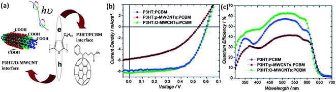 | ||
| Fig. 10 (a) Schematic for exciton generation, dissociation, and subsequent hole transfer to O-MWCNTs, (b) resulting J–V characteristics for reference, pristine carbon nanotubes and O-MWCNT incorporated devices and (c) the relevant EQE spectra (reproduced with permission from ref. 128, Copyright 2011, Wiley). | ||
Carbon nanotubes: electron or hole acceptor?
Despite widespread use of carbon nanotubes together with organic semiconductors, there appears to be a debate on the part of the scientific community as to what the role of the carbon nanotubes actually is. While certain groups claim nanotubes to be a hole transporter,121,127,128 others claim the nanotubes to be an electron transporter.123,129,130 Furthermore, there exists contradictory evidence, both electrically and optically for the preferred charge transportation through nanotubes under the same mechanisms. For example, while Schuettfort et al.130 have claimed an electron transfer from rr-P3HT to s-SWNTs with a (6,5) chirality, Dabera et al.24 as well as Dissanayake and Zhong122 have put forward strong experimental evidence for hole transfer to nanotubes from P3HT based on electrical measurements under controlled conditions (Fig. 11). Furthermore, Ham et al.131 studying planar photovoltaic devices based on heterojunctions formed between rr-P3HT and SWNTs grown parallel on the SiO2 (500 nm)/Si substrate have indicated the need for doping of the nanotubes in order to convert it to n-type. However, it is highly unlikely that such properties can be generalised to all conditions used. Therefore, it is crucial that an understanding of the charge transport properties is achieved prior to incorporation of nanotubes as a donor or acceptor in organic systems. Furthermore, such ambiguity, especially with SWNTs suggests the importance of investigations onto controlled doping of nanotubes through suitable treatments.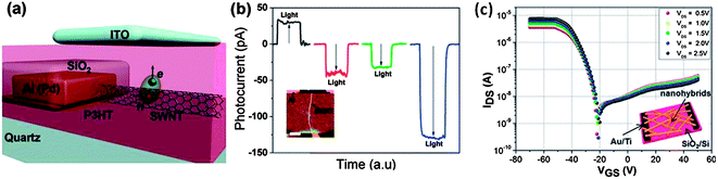 | ||
| Fig. 11 (a) Schematic for the hole transfer to SWNTs from rr-P3HT, (b) short circuit currents for individual s-SWNT/rr-P3HT junction (red line), m-SWNT/rr-P3HT junction (green line), an ensemble of SWNTs/rr-P3HT (blue line) and Al/P3HT references (black line) (reproduced with permission from ref. 122, Copyright 2010, American Chemical Society). With the current being collected from the ITO electrode, the resulting characteristics indicate a hole transfer to the nanotubes. (c) Field effect measurements carried out on rr-P3HT/s-SWNT nanohybrids in a N2 atmosphere indicating the p-type nature of such nanohybrids (reproduced with permission from ref. 24, Copyright 2013, American Chemical Society). | ||
Tuning the transport properties of carbon nanotubes for organic photovoltaics
One of the principal reasons behind the widespread use of MWNTs in place of SWNTs has been due to their uniformity of electronic properties. While pristine MWNTs are generally regarded to have work function (Φ) of ∼4.8 eV,122 photoelectron spectroscopic as well as Kelvin probe measurements have revealed a higher Φ of 5–5.1 eV for O-MWNTs.96,126 Tuning of Φ is likely to facilitate selective charge transport through the nanotubes. Much like Si, CNTs have been found to be doped p or n type through the incorporation of group III or group V elements into defect sites created in the tube. In this regard, boron (B) and nitrogen (N) doping has been reported132 due to the ease with which such elements can be incorporated into the nanotube structure.With regards to utilisation of such dopants, one of the first reports is the work of Lee et al.132 where either B doped MWNTs (B-CNT) or N doped MWNTs (N-CNTs) or both were incorporated into active layers consisting of rr-P3HT:PC71BM. Analysis of electron and hole only devices revealed a more balanced charge transport upon the incorporation of nanotubes. This highlights the importance of adding inorganic components to balance charge extraction in organic systems where electron and hole mobilities are generally known to be unbalanced. Furthermore, the above work has also revealed that addition of either B-CNTs or N-CNTs can improve the PCE significantly to 4.1% and 3.7%, respectively, with respect to a reference device performance of 3%. Taking the above work a step further, Lee et al.133 have attached InP quantum dots to N-CNTs, where the InP:N-CNTs, much like in the work of Nismy et al.,128 are utilised to improve exciton dissociation and charge transfer (in this case, electrons) into the nanotubes. Incorporation of InP:N-CNTs into active layers of rr-P3HT:IC61BA under optimised conditions lead to a significant improvement in the PCE of the devices from 4.68% to 6.11%, principally driven by improved exciton dissociation and fill factor as a result of balanced charge transport. Recently, the work on incorporation of carbon nanotubes has been expanded into low band gap polymers. In this regard, Lu et al.134 have incorporated N-MWNTs into active layers based on PTB7:PC71BM which led to an improvement in the PCE from 7.3% to 8.6% through tuning of the nanotube concentration. In that work, the observed improvement was attributed to increased light coupling, exciton dissociation and charge transport as a result of incorporation of nanotubes into the active layer.
Carbon nanotubes and organic solar cells over the years
Developments over the past 15 years have led to a better understanding on the role of CNTs in organic optoelectronic devices. Combined with the recent developments in dispersion techniques for CNTs, this has led to CNTs being successfully incorporated as active components in organic photovoltaic systems that has led to improvements in power conversion efficiencies as evident from the results presented in Table 1.| Year | Architecture | V OC (V) | J SC (mA cm−2) | FF (%) | PCE (%) | Device area (cm2) | Spectrum/(mW cm−2) | Ref. |
|---|---|---|---|---|---|---|---|---|
| 2002 | ITO/P3OT/P3OT:SWNT/Al | 0.75 | 0.12 | 40 | 0.04 | — | AM1.5G/100 | 123 |
| 2006 | ITO/PEDOT:PSS/PTEBS:MWNT/C60/Al | 0.57 | 1.52 | 62 | 0.55 | 0.1 | AM1.5G/100 | 126 |
| 2007 | ITO/PEDOT:PSS/rr-P3HT:PC61BM:MWNT/LiF/Al | 0.57 | 9.33 | 38 | 2.00 | 0.28 | AM1.5G/100 | 127 |
| 2007 | ITO/PEDOT:PSS/rr-P3HT:C60:SWNT/LiF/Al | 0.54 | 2.69 | 49 | 0.75 | 0.16 | AM1.5G/95 | 135 |
| 2008 | ITO/PEDOT:PSS/rr-P3HT:SWNT/Al | 0.48 | 1.93 | 43 | 0.52 | 0.25 | -/70 | 136 |
| 2008 | ITO/PEDOT:PSS/rr-P3HT:PC61BM:SWNT/Al | 0.55 | 4.95 | 52 | 1.40 | 0.05 | AM1.5G/100 | 137 |
| 2009 | ITO/PEDOT:PSS/QTF12:PC61BM:DWNT/BCP/Al | 0.56 | 2.37 | 37 | 0.50 | 0.28 | AM1.5G/100 | 138 |
| 2010 | ITO/PEDOT:PSS/rr-P3HT:PC61BM:MWNT/BCP/Al | 0.60 | 6.00 | 62 | 2.00 | 0.76 | AM1.5G/100 | 15 |
| 2011 | ITO/PEDOT:PSS/rr-P3HT:PC71BM:MWNT/LiF/Al | 0.60 | 8.34 | 61 | 3.05 | 0.76 | AM1.5G/100 | 128 |
| 2011 | ITO/PEDOT:PSS/rr-P3HT:IC61BA:B-CNT/TiOx/Al | 0.57 | 11.47 | 61 | 4.1 | 0.04 | AM1.5G/100 | 132 |
| 2013 | ITO/PEDOT:PSS/rr-P3HT:IC61BA:QD:N-CNT/TiOx/Al | 0.79 | 11.9 | 65 | 6.1 | 0.04 | AM1.5G/100 | 133 |
| 2013 | ITO/PEDOT:PSS/PTB7:PC71BM:N-MWNT/Ca/Al | 0.70 | 17.70 | 68.4 | 8.6 | 0.0314 | AM1.5G/100 | 134 |
Optical enhancements through plasmonics
In the previous section, routes for improvement of charge transport through incorporation of carbon nanotubes were discussed. Other than improved carrier mobility, another factor that improves the overall exciton and photocurrent generation is the light coupling into the active layer. This tends to be poor as a result of the extremely thin nature of the photoactive layers. Various techniques, initially based on Si PV technology, have been introduced into organic photovoltaic devices in order to improve the light coupling into active layers.139 Of these, the concept of Surface Plasmon Polaritons (SPP) is considered to be the most promising. SPPs are defined as the collective oscillation of electrons at the interface between metallic nanoparticles and a semiconductor or a dielectric. With the intensity of such oscillations decaying exponentially within distances of ten to hundreds of nanometers, such effects have been suggested to be useful in improving the light coupling into thin organic active layer. Furthermore, the lower refractive indices of organic materials systems allows better overlap of the SPP resonance with the AM 1.5G solar spectrum, which has led to expectations for improvement in the performance of thin film PVs and especially polymer solar cells in general. Due to the thin nature of the active layers used in polymer solar cells, the majority of research on incorporation of plasmonic effects has focused on the integration of metallic nanoparticles140,141 or backgrated electrodes.117,142 As this review intends to focus on 4G PVs, the focus will be on the effects of incorporation of nanoparticles.The optical effects on the incorporation of mNPs into polymer solar cells are known to be dependent on the particle size. For mNPs whose size is less than ∼20 nm, the nanoparticles are expected to lead to near field enhancements that improve the absorption cross-section of the active layer.143 On the other hand, mNPs larger than 40 nm act as light scattering sites increasing the optical absorption.140 However, while this suggests that incorporation of mNPs can positively affect the absorption, the inclusion of such nanoparticles into the active layer is likely to lead to quenching of photogenerated excitons, thereby leading to the degradation of the device performance. On the other hand, due to the excellent charge transport properties of metallic nanoparticles, the addition of such nanoparticles into the active layer is expected to lead to improved carrier extraction. Therefore, identification of suitable nanoparticle size and concentration is important in improving the device performance.
Incorporation of metallic nanoparticles to the active layer
As stated previously, mNPs in a suitable dielectric environment can act as sub-wavelength antennas, increasing the absorption cross-section, or lead to light scattering effects, producing longer optical path lengths within the active layer. The incorporation of such mNPs, especially Au and Ag has been reported for a range of active layers including rr-P3HT:PC71BM (Au mNPs, increased PCE from 3.54% to 4.36%), [(4,4′-bis(2-ethylhexyl)dithieno[3,2-b:2′,3′-d]silole)-2,6-diyl-alt-(4,7-bis(2-thienyl)-2,1,3-benzothiadiazole)-5,5′-diyl] (Si-PCPDTBT):PC71BM (Au mNPs, increased PCE from 3.92% to 4.54%), PCDTBT:PC70BM (Au mNPs, increased PCE from 5.77% to 6.45% (ref. 141) (Fig. 12) or Ag mNPs, increased PCE from 6.3% to 7.1% (ref. 140)). In the majority of these cases, the mNPs used have been sufficiently large that optical absorption is improved as a result of increased optical path length (Fig. 13). | ||
| Fig. 12 (a) and (b) J–V and EQE characteristics for optimised B-CNT and N-CNT incorporated rr-P3HT:PCBM PSCs (reproduced with permission from ref. 132, Copyright 2010, Wiley). (c and d) J–V and EQE characteristics for N-CNT incorporated PTB7:PC71BM incorporated PSCs. (e) Scanning electron micrograph of N-CNTs in the PTB7:PC71BM active layer (reproduced with permission from ref. 134, Copyright 2013, American Chemical Society). | ||
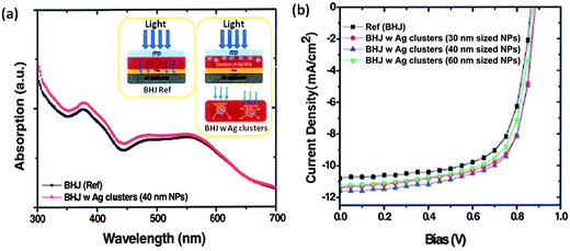 | ||
| Fig. 13 (a) Enhancement in optical absorption through the visible spectrum for PCDTBT:PC71BM active layers through incorporation of Ag nanoparticles and (b) the J–V characteristics for PCDTBT:PC71BM with Ag NPs of different sizes (reproduced with permission from ref. 140, Copyright 2011, Wiley). | ||
In addition to the optical effects, the incorporation of mNPs is known to have an impact on the charge transport properties of the active layer. However, there appears to be contradictory results in the literature. For example, Wang et al.140 suggests an improvement in carrier extraction supported by a drop in series resistance and improved short circuit current density. On the other hand, Xue et al.144 claims an improvement in mobility due to mNPs, but a loss in carrier extraction due to mNPs acting as charge trapping sites. Again as is the case for 4G solar cells incorporating inorganic components in the active layer, such results cannot be generalised for all. It is highly likely that such losses (both due to exciton quenching as well as charge trapping) can be mitigated through a detailed understanding of the concentration, shape and size effects of mNPs in the active layer.
6 Outlook for 4G solar cells
Recent investigations on 3G polymer solar cells have indicated the possibility of exceeding the 9% PCE for single junction cells145 and 10% for tandem structures146 based on inverted architectures. Such developments are based on the utilisation of inverted device architectures which allows the tailoring of light coupling into the active layer, due to the wider range of electron transport layers available, as well as the development of low bandgap NIR absorbing high performance polymers. Despite the promise shown, the progress achieved is still likely to be limited due to the problems outlined previously in this review: the requirement for thinner active layers due to the low mobility of polymers and the resulting poor optical absorption. Therefore, future investigations on improving the device performance should focus on the development of 4G architectures to mitigate such issues.Recently, there has been a cascade in the improvement of optical coupling into active layers through the incorporation of plasmonic nanostructures. While it is becoming increasingly evident that such structures are useful in light coupling into single junction devices, developments are required if the same design aspects are to be incorporated into multijunction devices. Recently, Beliatis et al.94 has indicated the possibility of tuning the plasmon resonance peaks through the formation of metal alloy nanoparticles. Such metal nanoparticles could be an important addition to multijunction photovoltaic cells where light coupling needs to be improved in each cell without compromising the light transmission to the lower bandgap cells. This could result in improving optical coupling to individual layers, as well as improving charge transport.
In addition to the above mNPs, another promising area for investigation is carbon nanotubes incorporation. While tuning of carbon nanotubes has shown promise for tuning the charge transport within the active layers, carbon nanotubes have also been shown to be an effective, solution processable, replacement for traditional transport layers such as PEDOT:PSS. Furthermore, there is also promise in the production of hybrid architectures involving metal oxide/carbon nanostructures as transport layers. While the first reports are now appearing in the scientific literature, the majority of research on such nanostructures is limited to dye sensitized solar cells.
It is interesting to note that despite the increasingly evident enhancements in PCEs due to “inorganics-in-organics” such as those displayed in Fig. 14 for 4G solar cells with CNTs; there is still a lack of device certification from reputable institutions such as NREL. Device certification is of paramount importance, especially for a technology which is beginning to display promise in order to generate visibility of the PCE enhancements as well as to promote the possibility of commercialisation of 4G PV technology. All in all, it is more than likely that such nanohybrids will play a key role in improving light coupling, stability and improved charge extraction in PSCs. The days are numbered at present as to when the next single junction nano-hybrid will break the 10% power conversion efficiency, which should open the gates to a knowledge driven economy.
![Improvement in PCE for 4G polymer solar cells utilising carbon nanotubes. The references on which the PCEs are based on are given in brackets, [ref. 132] Lee et al., [ref. 24] Dabera et al., [ref. 131] Ham et al., [ref. 130] Schuettfort et al., [ref. 126] Miller et al., [ref. 125] Pradhan et al., [ref. 124] Scharber et al., and [ref. 121] Ago et al.](/image/article/2013/NR/c3nr02733c/c3nr02733c-f14.gif) | ||
| Fig. 14 Improvement in PCE for 4G polymer solar cells utilising carbon nanotubes. The references on which the PCEs are based on are given in brackets, [ref. 132] Lee et al., [ref. 24] Dabera et al., [ref. 131] Ham et al., [ref. 130] Schuettfort et al., [ref. 126] Miller et al., [ref. 125] Pradhan et al., [ref. 124] Scharber et al., and [ref. 121] Ago et al. | ||
7 Conclusions
A comprehensive review has been carried out for 4G PSCs based on carbon nanostructures, mNPs, metal oxides and nanohybrids. The versatile nature of such inorganic nanostructures has led to them being incorporated throughout the PSC architecture, including transport layers, active layer and electrodes, with the expectation that they will lead to more efficient, stable devices. In this regard, carbon nanostructures are widely regarded as ideal candidates for improving charge transport properties within the active layer while suitably engineered metal nanoparticles allow improvement of optical coupling in addition to charge transport. The immense promise of these new device architectures pave the way towards achieving high performance levels for PSCs to rival that of efficient inorganic systems.Acknowledgements
The authors acknowledge the support received from the EU FP7 programme SMARTONICS and E.ON AG. The authors are also grateful to EPSRC for the Postdoctoral Fellowships and the other grant funding awarded. The responsibility for the content published lies with the authors.Notes and references
- A. A. D. T. Adikaari, D. M. N. M. Dissanayake and S. R. P. Silva, IEEE J. Sel. Top. Quantum Electron., 2010, 16, 1595–1606 CrossRef.
- M. A. Green, Prog. Photovoltaics, 2001, 9, 123–135 CAS.
- G. Yu, J. Gao, J. C. Hummelen, F. Wudl and A. J. Heeger, Science, 1995, 270, 1789–1791 CAS.
- B. A. Collins, Z. Li, J. R. Tumbleston, E. Gann, C. R. McNeill and H. Ade, Adv. Energy Mater., 2013, 3, 65–74 CrossRef CAS.
- H. Hoppe and N. S. Sariciftci, J. Mater. Chem., 2006, 16, 45–61 RSC.
- J. A. Bartelt, Z. M. Beiley, E. T. Hoke, W. R. Mateker, J. D. Douglas, B. A. Collins, J. R. Tumbleston, K. R. Graham, A. Amassian, H. Ade, J. M. J. Frechet, M. F. Toney and M. D. McGehee, Adv. Energy Mater., 2013, 3, 364–374 CrossRef CAS.
- S. E. Shaheen, C. J. Brabec, N. S. Sariciftci, F. Padinger, T. Fromherz and J. C. Hummelen, Appl. Phys. Lett., 2001, 78, 841–843 CrossRef CAS.
- G. Li, V. Shrotriya, J. S. Huang, Y. Yao, T. Moriarty, K. Emery and Y. Yang, Nat. Mater., 2005, 4, 864–868 CrossRef CAS.
- J. Y. Kim, S. H. Kim, H. H. Lee, K. Lee, W. L. Ma, X. Gong and A. J. Heeger, Adv. Mater., 2006, 18, 572–576 CrossRef CAS.
- D. Muhlbacher, M. Scharber, M. Morana, Z. G. Zhu, D. Waller, R. Gaudiana and C. Brabec, Adv. Mater., 2006, 18, 2931 CrossRef.
- Y. Y. Liang, Z. Xu, J. B. Xia, S. T. Tsai, Y. Wu, G. Li, C. Ray and L. P. Yu, Adv. Mater., 2010, 22, E135–E138 CrossRef CAS.
- Y. M. Sun, C. J. Takacs, S. R. Cowan, J. H. Seo, X. Gong, A. Roy and A. J. Heeger, Adv. Mater., 2011, 23, 2226–2230 CrossRef CAS.
- L. T. Dou, J. Gao, E. Richard, J. B. You, C. C. Chen, K. C. Cha, Y. J. He, G. Li and Y. Yang, J. Am. Chem. Soc., 2012, 134, 10071–10079 CrossRef CAS.
- M. K. Riede, T. Mueller, B. Maennig, K. Leo, K. O. Sylvester-Hvid, B. Zimmermann, M. Niggemann and A. Gombert, Appl. Phys. Lett., 2008, 92, 076101 CrossRef.
- N. A. Nismy, A. A. D. T. Adikaari and S. R. P. Silva, Appl. Phys. Lett., 2010, 97, 033105 CrossRef.
- J. Gilot, I. Barbu, M. M. Wienk and R. A. J. Janssen, Appl. Phys. Lett., 2007, 91, 113520 CrossRef.
- Q. Gan, F. J. Bartoli and Z. H. Kafafi, Adv. Mater., 2013, 25, 2385–2396 CrossRef CAS.
- T. Gershon, Mater. Sci. Technol., 2011, 27, 1357–1371 CrossRef CAS.
- C. Bounioux, E. A. Katz and R. Yerushalmi-Rozen, Polym. Adv. Technol., 2012, 23, 1129–1140 CrossRef CAS.
- X. Yang, C.-C. Chueh, C.-Z. Li, H.-L. Yip, P. Yin, H. Chen, W.-C. Chen and A. K. Y. Jen, Adv. Energy Mater., 2013, 3, 666–673 CrossRef CAS.
- S. Iijima, Nature, 1991, 354, 56–58 CrossRef CAS.
- R. Saito, G. Dresselhaus and M. S. Dresselhaus, Physical properties of carbon nanotubes, Imperial College Press, London, 1998 Search PubMed.
- A. Nish, J. Y. Hwang, J. Doig and R. J. Nicholas, Nat. Nanotechnol., 2007, 2, 640–646 CrossRef CAS.
- G. D. M. R. Dabera, K. D. G. I. Jayawardena, M. R. R. Prabhath, I. Yahya, Y. Y. Tan, N. A. Nismy, H. Shiozawa, M. Sauer, G. Ruiz-Soria, P. Ayala, V. Stolojan, A. A. D. T. Adikaari, P. D. Jarowski, T. Pichler and S. R. P. Silva, ACS Nano, 2013, 7, 556–565 CrossRef CAS.
- M. C. Hersam, Nat. Nanotechnol., 2008, 3, 387–394 CrossRef CAS.
- P. C. Ma, N. A. Siddiqui, G. Marom and J. K. Kim, Composites, Part A, 2010, 41, 1345–1367 CrossRef.
- A. Javey, J. Guo, Q. Wang, M. Lundstrom and H. J. Dai, Nature, 2003, 424, 654–657 CrossRef CAS.
- Z. He, C. Zhong, X. Huang, W.-Y. Wong, H. Wu, L. Chen, S. Su and Y. Cao, Adv. Mater., 2011, 23, 4636–4643 CrossRef CAS.
- K. S. Novoselov, A. K. Geim, S. V. Morozov, D. Jiang, Y. Zhang, S. V. Dubonos, I. V. Grigorieva and A. A. Firsov, Science, 2004, 306, 666–669 CrossRef CAS.
- A. S. Mayorov, R. V. Gorbachev, S. V. Morozov, L. Britnell, R. Jalil, L. A. Ponomarenko, P. Blake, K. S. Novoselov, K. Watanabe, T. Taniguchi and A. K. Geim, Nano Lett., 2011, 11, 2396–2399 CrossRef CAS.
- Y. Y. Tan, K. D. G. I. Jayawardena, A. A. D. T. Adikaari, L. W. Tan, J. V. Anguita, S. J. Henley, V. Stolojan, J. D. Carey and S. R. P. Silva, Carbon, 2012, 50, 668–673 CrossRef CAS.
- Y. Y. Tan, L. W. Tan, K. D. G. I. Jayawardena, J. V. Anguita, J. D. Carey and S. R. P. Silva, Synth. Met., 2011, 161, 2249–2252 CrossRef CAS.
- H. Park, P. R. Brown, V. Buloyic and J. Kong, Nano Lett., 2012, 12, 133–140 CrossRef CAS.
- J. B. Wu, M. Agrawal, H. A. Becerril, Z. N. Bao, Z. F. Liu, Y. S. Chen and P. Peumans, ACS Nano, 2010, 4, 43–48 CrossRef CAS.
- F. Torrisi, T. Hasan, W. Wu, Z. Sun, A. Lombardo, T. S. Kulmala, G.-W. Hsieh, S. Jung, F. Bonaccorso, P. J. Paul, D. Chu and A. C. Ferrari, ACS Nano, 2012, 6, 2992–3006 CrossRef CAS.
- K. D. G. I. Jayawardena, J. Fryar, S. Ravi, P. Silva and S. J. Henley, J. Phys. Chem. C, 2010, 114, 12931–12937 CAS.
- S. Cho, K. Lee and A. J. Heeger, Adv. Mater., 2009, 21, 1941–1944 CrossRef CAS.
- L. B. Hu, H. Wu and Y. Cui, MRS Bull., 2011, 36, 760–765 CrossRef CAS.
- A. Kumar and C. W. Zhou, ACS Nano, 2010, 4, 11–14 CrossRef CAS.
- L. Brand, ObservatoryNANO, EU, 2012 Search PubMed.
- J. R. Sheats and D. B. Roitman, Synth. Met., 1998, 95, 79–85 CrossRef CAS.
- H. Aziz and Z. D. Popovic, Chem. Mater., 2004, 16, 4522–4532 CrossRef CAS.
- S. Choi, W. J. Potscavage and B. Kippelen, Opt. Express, 2010, 18, A458–A466 CrossRef CAS.
- Y. S. Eo, H. W. Rhee, B. D. Chin and J. W. Yu, Synth. Met., 2009, 159, 1910–1913 CrossRef CAS.
- T. Minami, Semicond. Sci. Technol., 2005, 20, S35–S44 CrossRef CAS.
- D. S. Ghosh, T. L. Chen and V. Pruneri, Appl. Phys. Lett., 2010, 96, 041109 CrossRef.
- J. S. Yu, I. Kim, J. S. Kim, J. Jo, T. T. Larsen-Olsen, R. R. Sondergaard, M. Hosel, D. Angmo, M. Jorgensen and F. C. Krebs, Nanoscale, 2012, 4, 6032–6040 RSC.
- Z. C. Wu, Z. H. Chen, X. Du, J. M. Logan, J. Sippel, M. Nikolou, K. Kamaras, J. R. Reynolds, D. B. Tanner, A. F. Hebard and A. G. Rinzler, Science, 2004, 305, 1273–1276 CrossRef CAS.
- Y. Q. Sun and G. Q. Shi, J. Polym. Sci., Part B: Polym. Phys., 2013, 51, 231–253 CrossRef CAS.
- S. De, T. M. Higgins, P. E. Lyons, E. M. Doherty, P. N. Nirmalraj, W. J. Blau, J. J. Boland and J. N. Coleman, ACS Nano, 2009, 3, 1767–1774 CrossRef CAS.
- R. C. Tenent, T. M. Barnes, J. D. Bergeson, A. J. Ferguson, B. To, L. M. Gedvilas, M. J. Heben and J. L. Blackburn, Adv. Mater., 2009, 21, 3210–3216 CrossRef CAS.
- L. G. De Arco, Y. Zhang, C. W. Schlenker, K. Ryu, M. E. Thompson and C. W. Zhou, ACS Nano, 2010, 4, 2865–2873 CrossRef.
- S. Y. Chou and W. Ding, Opt. Express, 2013, 21, A60–A76 CrossRef CAS.
- C. A. Mills, F. L. M. Sam, A. S. Alshammari, L. J. Rozanski, N. G. Emerson and S. R. P. Silva, submitted to IEEE Journal of Display Technology.
- J. Y. Lee, S. T. Connor, Y. Cui and P. Peumans, Nano Lett., 2008, 8, 689–692 CrossRef CAS.
- S. Coskun, E. S. Ates and H. E. Unalan, Nanotechnology, 2013, 24, 125202 CrossRef.
- T. Durkop, S. A. Getty, E. Cobas and M. S. Fuhrer, Nano Lett., 2004, 4, 35–39 CrossRef.
- P. Poncharal, C. Berger, Y. Yi, Z. L. Wang and W. A. de Heer, J. Phys. Chem. B, 2002, 106, 12104–12118 CrossRef CAS.
- K. S. Kim, Y. Zhao, H. Jang, S. Y. Lee, J. M. Kim, K. S. Kim, J. H. Ahn, P. Kim, J. Y. Choi and B. H. Hong, Nature, 2009, 457, 706–710 CrossRef CAS.
- S. Bae, H. Kim, Y. Lee, X. F. Xu, J. S. Park, Y. Zheng, J. Balakrishnan, T. Lei, H. R. Kim, Y. I. Song, Y. J. Kim, K. S. Kim, B. Ozyilmaz, J. H. Ahn, B. H. Hong and S. Iijima, Nat. Nanotechnol., 2010, 5, 574–578 CrossRef CAS.
- C. Mattevi, H. Kim and M. Chhowalla, J. Mater. Chem., 2011, 21, 3324–3334 RSC.
- T. Kobayashi, M. Bando, N. Kimura, K. Shimizu, K. Kadono, N. Umezu, K. Miyahara, S. Hayazaki, S. Nagai, Y. Mizuguchi, Y. Murakami and D. Hobara, Appl. Phys. Lett., 2013, 102, 023112 CrossRef.
- V. C. Tung, L. M. Chen, M. J. Allen, J. K. Wassei, K. Nelson, R. B. Kaner and Y. Yang, Nano Lett., 2009, 9, 1949–1955 CrossRef CAS.
- E. Van Kerschaver and G. Beaucarne, Prog. Photovoltaics, 2006, 14, 107–123 Search PubMed.
- M. Kaltenbrunner, M. S. White, E. D. Glowacki, T. Sekitani, T. Someya, N. S. Sariciftci and S. Bauer, Nat. Commun., 2012, 3, 770 CrossRef.
- D. H. Kim, M. R. Park, H. J. Lee and G. H. Lee, Appl. Surf. Sci., 2006, 253, 409–411 CrossRef CAS.
- E. Kymakis, E. Stratakis and E. Koudoumas, Thin Solid Films, 2007, 515, 8598–8600 CrossRef CAS.
- J. Li, L. Hu, L. Wang, Y. Zhou, G. Gruner and T. J. Marks, Nano Lett., 2006, 6, 2472–2477 CrossRef CAS.
- G. Gruner, J. Mater. Chem., 2006, 16, 3533–3539 RSC.
- M. G. Kang and L. J. Guo, Adv. Mater., 2007, 19, 1391–1396 CrossRef CAS.
- S. Gunes, H. Neugebauer and N. S. Sariciftci, Chem. Rev., 2007, 107, 1324–1338 CrossRef.
- M. De Jong, L. Van Ijzendoorn and M. De Voigt, Appl. Phys. Lett., 2000, 77, 2255–2257 CrossRef CAS.
- K. Kawano, R. Pacios, D. Poplavskyy, J. Nelson, D. D. C. Bradley and J. R. Durrant, Sol. Energy Mater. Sol. Cells, 2006, 90, 3520–3530 CrossRef CAS.
- S. Han, W. S. Shin, M. Seo, D. Gupta, S. J. Moon and S. Yoo, Org. Electron., 2009, 10, 791–797 CrossRef CAS.
- G. Li, C.-W. Chu, V. Shrotriya, J. Huang and Y. Yang, Appl. Phys. Lett., 2006, 88, 253503 CrossRef.
- Y. Sun, C. J. Takacs, S. R. Cowan, J. H. Seo, X. Gong, A. Roy and A. J. Heeger, Adv. Mater., 2011, 23, 2226–2230 CrossRef CAS.
- S.-Y. Park, H.-R. Kim, Y.-J. Kang, D.-H. Kim and J.-W. Kang, Sol. Energy Mater. Sol. Cells, 2010, 94, 2332–2336 CrossRef CAS.
- E. L. Ratcliff, B. Zacher and N. R. Armstrong, J. Phys. Chem. Lett., 2011, 2, 1337–1350 CrossRef CAS.
- J. Meyer, R. Khalandovsky, P. Görrn and A. Kahn, Adv. Mater., 2011, 23, 70–73 CrossRef CAS.
- T. Stubhan, I. Litzov, N. Li, H. Wang, J. Krantz, F. Machui, M. Steidl, H. Oh, G. Matt and C. Brabec, Proc. SPIE 8477, Organic Photovoltaics XIII, 84770J, September 27, 2012 Search PubMed.
- F. Liu, S. Shao, X. Guo, Y. Zhao and Z. Xie, Sol. Energy Mater. Sol. Cells, 2010, 94, 842–845 CrossRef CAS.
- C. Girotto, E. Voroshazi, D. Cheyns, P. Heremans and B. P. Rand, ACS Appl. Mater. Interfaces, 2011, 3, 3244–3247 CAS.
- C.-P. Chen, Y.-D. Chen and S.-C. Chuang, Adv. Mater., 2011, 23, 3859–3863 CAS.
- K. Zilberberg, S. Trost, J. Meyer, A. Kahn, A. Behrendt, D. Lützenkirchen-Hecht, R. Frahm and T. Riedl, Adv. Funct. Mater., 2011, 21, 4776–4783 CrossRef CAS.
- J. R. Manders, S.-W. Tsang, M. J. Hartel, T.-H. Lai, S. Chen, C. M. Amb, J. R. Reynolds and F. So, Adv. Funct. Mater., 2013, 2993 CrossRef CAS.
- K. Zilberberg, S. Trost, J. Meyer, A. Kahn, A. Behrendt, D. Lützenkirchen-Hecht, R. Frahm and T. Riedl, Adv. Funct. Mater., 2011, 21, 4776–4783 CrossRef CAS.
- J. J. Jasieniak, J. Seifter, J. Jo, T. Mates and A. J. Heeger, Adv. Funct. Mater., 2012, 22, 2594–2605 CrossRef CAS.
- F. Xie, W. C. H. Choy, C. Wang, X. Li, S. Zhang and J. Hou, Adv. Mater., 2013, 2051 CrossRef CAS.
- N. N. Lal, B. F. Soares, J. Sinha, F. Huang, S. Mahajan, P. Bartlett, N. Greenham and J. J. Baumberg, Opt. Express, 2011, 19(12), 11256–11263 CrossRef CAS.
- R. S. Kim, J. Zhu, J. H. Park, L. Li, Z. Yu, H. Shen, M. Xue, K. L. Wang, G. Park and T. J. Anderson, Opt. Express, 2012, 20, 12649–12657 CrossRef CAS.
- M. J. Beliatis, S. Henley, S. Han, K. Gandhi, D. Adikaari, E. Stratakis, E. Kymakis and P. S. R. P. Silva, Phys. Chem. Chem. Phys., 2013, 15, 8237 RSC.
- M. Grzelczak, J. Pérez-Juste, P. Mulvaney and L. M. Liz-Marzán, Chem. Soc. Rev., 2008, 37, 1783–1791 RSC.
- G. V. Ramesh, S. Porel and T. P. Radhakrishnan, Chem. Soc. Rev., 2009, 38, 2646–2656 RSC.
- M. J. Beliatis, S. J. Henley and S. R. P. Silva, Opt. Lett., 2011, 36, 1362–1364 CrossRef CAS.
- J. W. Jo, J. W. Jung, J. U. Lee and W. H. Jo, ACS Nano, 2010, 4, 5382–5388 CrossRef CAS.
- R. A. Hatton, N. P. Blanchard, L. W. Tan, G. Latini, F. Cacialli and S. R. P. Silva, Org. Electron., 2009, 10, 388–395 CrossRef CAS.
- R. A. Hatton, N. P. Blanchard, V. Stolojan, A. J. Miller and S. R. P. Silva, Langmuir, 2007, 23, 6424–6430 CrossRef CAS.
- G. D. M. Dabera, K. I. Jayawardena, M. R. Prabhath, I. Yahya, Y. Y. Tan, N. A. Nismy, H. Shiozawa, M. Sauer, G. Ruiz-Soria and P. Ayala, ACS Nano, 2012, 7, 556 CrossRef.
- W. S. Hummers Jr and R. E. Offeman, J. Am. Chem. Soc., 1958, 80, 1339 CrossRef.
- S.-S. Li, K.-H. Tu, C.-C. Lin, C.-W. Chen and M. Chhowalla, ACS Nano, 2010, 4, 3169–3174 CrossRef CAS.
- J. M. Yun, J. S. Yeo, J. Kim, H. G. Jeong, D. Y. Kim, Y. J. Noh, S. S. Kim, B. C. Ku and S. I. Na, Adv. Mater., 2011, 23, 4923–4928 CrossRef CAS.
- J. M. Lee, J. S. Park, S. H. Lee, H. Kim, S. Yoo and S. O. Kim, Adv. Mater., 2011, 23, 629–633 CrossRef CAS.
- J. Liu, Y. Xue, Y. Gao, D. Yu, M. Durstock and L. Dai, Adv. Mater., 2012, 24, 549 CrossRef.
- S. H. Park, A. Roy, S. Beaupré, S. Cho, N. Coates, J. S. Moon, D. Moses, M. Leclerc, K. Lee and A. J. Heeger, Nat. Photonics, 2009, 3, 297–302 CrossRef CAS.
- Z. Liang, Q. Zhang, O. Wiranwetchayan, J. Xi, Z. Yang, K. Park, C. Li and G. Cao, Adv. Funct. Mater., 2012, 22, 2194–2201 CrossRef CAS.
- J. You, C. C. Chen, L. Dou, S. Murase, H. S. Duan, S. Hawks, T. Xu, H. J. Son, L. Yu, G. Li and Y. Yang, Adv. Mater., 2012, 38, 5267 CrossRef.
- H. Oh, J. Krantz, I. Litzov, T. Stubhan, L. Pinna and C. J. Brabec, Sol. Energy Mater. Sol. Cells, 2011, 95, 2194–2199 CrossRef CAS.
- D. H. Wang, J. K. Kim, J. H. Seo, I. Park, B. H. Hong, J. H. Park and A. J. Heeger, Angew. Chem., Int. Ed., 2013, 52, 2874–2880 CrossRef CAS.
- S. H. Jin, G. H. Jun, S. H. Hong and S. Jeon, Carbon, 2012, 50, 4483–4488 CrossRef CAS.
- A. J. Morfa, K. L. Rowlen, T. H. Reilly, M. J. Romero and J. van de Lagemaat, Appl. Phys. Lett., 2008, 92, 013504 CrossRef.
- S. S. Kim, S. I. Na, J. Jo, D. Y. Kim and Y. C. Nah, Appl. Phys. Lett., 2008, 93, 073307 CrossRef.
- J. H. Lee, J. H. Park, J. S. Kim, D. Y. Lee and K. Cho, Org. Electron., 2009, 10, 416–420 CrossRef CAS.
- F. C. Chen, J. L. Wu, C. L. Lee, Y. Hong, C. H. Kuo and M. H. Huang, Appl. Phys. Lett., 2009, 95, 013305 CrossRef.
- L. F. Qiao, D. Wang, L. J. Zuo, Y. Q. Ye, J. Qian, H. Z. Chen and S. L. He, Appl. Energy, 2011, 88, 848–852 CrossRef CAS.
- L. Y. Lu, Z. Q. Luo, T. Xu and L. P. Yu, Nano Lett., 2013, 13, 59–64 CrossRef CAS.
- S.-W. Baek, J. Noh, C.-H. Lee, B. Kim, M.-K. Seo and J.-Y. Lee, Sci. Rep., 2013, 3, 1726 CAS.
- X. H. Li, W. C. H. Choy, L. J. Huo, F. X. Xie, W. E. I. Sha, B. F. Ding, X. Guo, Y. F. Li, J. H. Hou, J. B. You and Y. Yang, Adv. Mater., 2012, 24, 3046–3052 CrossRef CAS.
- J. Yang, J. B. You, C. C. Chen, W. C. Hsu, H. R. Tan, X. W. Zhang, Z. R. Hong and Y. Yang, ACS Nano, 2011, 5, 6210–6217 CrossRef CAS.
- J. S. Moon, J. Jo and A. J. Heeger, Adv. Energy Mater., 2012, 2, 304–308 CrossRef CAS.
- J. D. Kotlarki and P. W. M. Blom, Appl. Phys. Lett., 2012, 100, 013306 CrossRef.
- H. Ago, K. Petritsch, M. S. P. Shaffer, A. H. Windle and R. H. Friend, Adv. Mater., 1999, 11, 1281–1285 CrossRef CAS.
- N. M. Dissanayake and Z. H. Zhong, Nano Lett., 2011, 11, 286–290 CrossRef CAS.
- E. Kymakis and G. A. J. Amaratunga, Appl. Phys. Lett., 2002, 80, 112–114 CrossRef CAS.
- M. C. Scharber, D. Wuhlbacher, M. Koppe, P. Denk, C. Waldauf, A. J. Heeger and C. L. Brabec, Adv. Mater., 2006, 18, 789–794 CrossRef CAS.
- B. Pradhan, S. K. Batabyal and A. J. Pal, Appl. Phys. Lett., 2006, 88, 093106 CrossRef.
- A. J. Miller, R. A. Hatton and S. R. P. Silva, Appl. Phys. Lett., 2006, 89, 133117 CrossRef.
- S. Berson, R. de Bettignies, S. Bailly, S. Guillerez and B. Jousselme, Adv. Funct. Mater., 2007, 17, 3363–3370 CrossRef CAS.
- N. A. Nismy, K. D. G. I. Jayawardena, A. A. D. T. Adikaari and S. R. P. Silva, Adv. Mater., 2011, 23, 3796–3800 CAS.
- E. Kymakis and G. A. J. Amaratunga, Rev. Adv. Mater. Sci., 2005, 10, 300–305 CAS.
- T. Schuettfort, A. Nish and R. J. Nicholas, Nano Lett., 2009, 9, 3871–3876 CrossRef CAS.
- M. H. Ham, G. L. C. Paulus, C. Y. Lee, C. Song, K. Kalantar-zadeh, W. Choi, J. H. Han and M. S. Strano, ACS Nano, 2010, 4, 6251–6259 CrossRef CAS.
- J. M. Lee, J. S. Park, S. H. Lee, H. Kim, S. Yoo and S. O. Kim, Adv. Mater., 2011, 23, 629–633 CrossRef CAS.
- J. M. Lee, B.-H. Kwon, H. I. Park, H. Kim, M. G. Kim, J. S. Park, E. S. Kim, S. Yoo, D. Y. Jeon and S. O. Kim, Adv. Mater., 2013, 25, 2011–2017 CrossRef CAS.
- L. Lu, T. Xu, W. Chen, J. M. Lee, Z. Luo, I. H. Jung, H. I. Park, S. O. Kim and L. Yu, Nano Lett., 2013, 13, 2151 CrossRef.
- C. Li and S. Mitra, Appl. Phys. Lett., 2007, 91, 253112 CrossRef.
- M. Lanzi, L. Paganin and D. Caretti, Polymer, 2008, 49, 4942–4948 CrossRef CAS.
- E. Kymakis, N. Kornilios and E. Koudoumas, J. Phys. D: Appl. Phys., 2008, 41, 165110 CrossRef.
- L. Picard, F. Lincker, Y. Kervella, M. Zagorska, R. DeBettignies, A. Peigney, E. Flahaut, G. Louarn, S. Lefrant, R. Demadrille and A. Pron, J. Phys. Chem. C, 2009, 113, 17347–17354 CAS.
- H. A. Atwater and A. Polman, Nat. Mater., 2010, 9, 865 CrossRef CAS.
- D. H. Wang, K. H. Park, J. H. Seo, J. Seifter, J. H. Jeon, J. K. Kim, J. H. Park, O. O. Park and A. J. Heeger, Adv. Energy Mater., 2011, 1, 766–770 CrossRef CAS.
- D. H. Wang, D. Y. Kim, K. W. Choi, J. H. Seo, S. H. Im, J. H. Park, O. O. Park and A. J. Heeger, Angew. Chem., Int. Ed., 2011, 50, 5519–5523 CrossRef CAS.
- J. B. You, X. H. Li, F. X. Xie, W. E. I. Sha, J. H. W. Kwong, G. Li, W. C. H. Choy and Y. Yang, Adv. Energy Mater., 2012, 2, 1203–1207 CrossRef CAS.
- J. Wang, Y. J. Lee, A. S. Chadha, J. Yi, M. L. Jespersen, J. J. Kelley, H. M. Nguyen, M. Nimmo, A. V. Malko, R. A. Vaia, W. D. Zhou and J. W. P. Hsu, J. Phys. Chem. C, 2013, 117, 85–91 CAS.
- M. Xue, L. Li, B. J. T. de Villers, H. J. Shen, J. F. Zhu, Z. B. Yu, A. Z. Stieg, Q. B. Pei, B. J. Schwartz and K. L. Wang, Appl. Phys. Lett., 2011, 98, 253302 CrossRef.
- Z. He, C. Zhong, S. Su, M. Xu, H. Wu and Y. Cao, Nat. Photonics, 2012, 6, 593–597 CrossRef CAS.
- J. B. You, L. T. Dou, K. Yoshimura, T. Kato, K. Ohya, T. Moriarty, K. Emery, C. C. Chen, J. Gao, G. Li and Y. Yang, Nat. Commun., 2013, 4, 1446 CrossRef.
| This journal is © The Royal Society of Chemistry 2013 |