DOI:
10.1039/C3NR02635C
(Paper)
Nanoscale, 2013,
5, 10376-10383
Electrodeposited three-dimensional Ni–Si nanocable arrays as high performance anodes for lithium ion batteries†
Received 21st May 2013, Accepted 9th August 2013
First published on 15th August 2013
Abstract
A configuration of three-dimensional Ni–Si nanocable array anodes is proposed to overcome the severe volume change problem of Si during the charging–discharging process. In the fabrication process, a simple and low cost electrodeposition is employed to deposit Si instead of the common expansive vapor phase deposition methods. The optimum composite nanocable array electrode achieves a high specific capacity ∼1900 mA h g−1 at 0.05 C. After 100 cycles at 0.5 C, 88% of the initial capacity (∼1300 mA h g−1) remains, suggesting its good capacity retention ability. The high performance of the composite nanocable electrode is attributed to its excellent adhesion of the active material on the three-dimensional current collector and short ionic/electronic transport pathways during cycling.
Introduction
In recent years, nanostructured Si has been demonstrated to overcome the most critical problem of bulk Si in serving as Li-ion battery (LIB) anodes, that is, severe volume expansion and thus high stress induced during the lithiation process.1,2 Several unique characteristics of the nanostructured Si contribute to the release of the stress built. Nanostructured configurations are always associated with abundant interspace and/or voids, which can accommodate the volume expansion of Si during lithiation.3–6 It has also been found that the small size of Si helps release mechanical strain during cycling.7 In this way, the structural stability of the electrode is enhanced, resulting in a great improvement in capacity retention. In addition, nanostructured electrodes also provide shortened transport pathways for Li and electrons, improving the rate capabilities during the discharging–charging process.5,6Two common configurations have been employed using nanostructured Si as the active material for LIB anodes. The first one utilizes free standing nanomaterials (e.g. nanoparticles, nanowires etc.), and relies on binders/additives to provide mechanical support and enhance electrical contact.3,5,8 Nevertheless, the introduction of binders and additives generates undesired interfaces, which increases the complexity of charge transfer during the discharging–charging process.9 The second one takes nanostructured Si directly grown on current collectors (e.g. carbon nanotubes or metallic nanostructures), being free of binders or additives.10–14 This is a more promising configuration, as it is simple and provides strong mechanical support. Further strain relaxation is also expected due to the presence of ductile current collectors.15 To maximize the electrical conductivity as well as the mechanical stability, an inactive metallic (that does not alloy with Li) current collector is desired.12–14,16
One the other hand, a commonly employed method to deposit Si on metallic substrates is via vapor phase deposition, such as chemical vapor deposition (CVD) and sputtering.3,4,12,14,17 Expansive equipment and/or toxic and flammable gases (e.g. silane) are usually involved in these deposition methods. More importantly, the Si layer deposited on topographical substrates suffers from significant non-uniformity due to shadow effects.18 A simple and low cost deposition method is highly desired, and electrodeposition is a promising one. A difficult problem associated with electrodeposited Si for LIBs is the estimation of Si mass, without which evaluation of the specific capacities is impossible and overestimation is commonly encountered. In electrodeposition, the mass of Si cannot be obtained simply from Faraday's law (current efficiency <100%)19 or by weighing the material in air after the electrodeposition (due to easy oxidation of electrodeposited Si).19,20
In the present work, three-dimensional (3D) Ni core–Si shell nanocable arrays are grown as LIB anodes. The metallic Ni nanowire arrays were firstly prepared as the current collector on a conductive substrate, before a thin layer of Si was electrodeposited onto the nanostructured current collector. The mass of the Si was indirectly determined after its being completely oxidized to SiO2. The composite nanocable array electrode exhibits considerable improvement in electrochemical performance when compared to its thin film counterpart of the same mass. Moreover, an optimal thickness of the Si shell is identified for improved rate performance.
Experimental section
Preparation of the metallic Ni nanowire arrays on a conducting substrate
The growth method of the metallic Ni nanowire arrays was modified from a literature report.21 Briefly, a Ni foil (0.9 mm × 0.9 mm, 0.5 mm thick, 99% purity, Goodfellow) substrate was mechanically polished and carefully cleaned. Then a stack consisting of a polished Ni foil cathode, an anodic aluminum oxide (AAO, Anodisc 13, Whatman), a filter paper (215 μm thick, mean porous diameter 20 μm, Grade 40, Whatman), and a Ni foil anode was immersed into an electrolytic bath (350 g L−1 NiSO4·6H2O, and 45 g L−1 H3BO3). A two-step pulsed cathodic current profile (step 1, −0.002 A, 0.25 s; step 2, −0.03 A, 0.05 s; 2000 cycles) was used to deposit the Ni nanowire arrays. After that, the AAO template was removed by a 3 M NaOH solution at 80 °C. At last, to increase the separation distance between individual Ni nanowires, the sample was electropolished in an acid solution (60% v/v H3PO4, 20% v/v H2SO4, 20% v/v H2O) at room temperature. A two-step pulsed anodic voltage profile (step 1, 0 V, 10 s; step 2, 4 V, 0.08 s; 20 cycles) was used in the electrochemical polishing process.Si electrodeposition on the metallic Ni nanowire arrays
Si was electrodeposited on the Ni nanowire arrays using a three-electrode system in a non-aqueous electrolyte solution.20,22 The metallic Ni nanowire arrays, Pt foil, and Pt wire were used as the corresponding working electrode, counter electrode, and quasi-reference electrode. Before assembling the electrodes, the back side (without Ni nanowire arrays) of the Ni foil was covered with teflon adhesive tape. The electrolyte solution consisted of 0.5 M tetrachlorosilane (SiCl4, 99.998%, Sigma-aldrich) and 0.1 M tetrabutylammonium chloride (TBACl, ≥99.0%, Fluka) in 20 ml propylene carbonate (PC, anhydrous, 99.7%, Sigma-aldrich). The electrodeposition of Si was carried out under a constant current density (−1 mA cm−2) at room temperature in an argon-filled dry glove box (H2O < 0.1 ppm, O2 < 0.1 ppm, M. Braun Inertgas Systems Co., Ltd.). After drying, a brownish yellow deposited layer was observed. Finally, the electrodeposited Si samples were heated at 350 °C for 30 minutes in the glove box. To determine the mass of the active materials on the substrate, the samples were weighed before and after complete oxidation (90 °C in air for ∼10 days) by a semi-micro analytical balance (AEG-80SM, Shimadzu, readability: 0.01 mg). More details of the mass calculation of the active material are discussed in the results and discussion section.Characterizations
The crystallinity of the samples was examined by X-ray diffraction (XRD, SmartLab, Rigaku) with a Cu Kα radiation source (d = 0.1541 nm). The morphologies and the chemical compositions were characterized by a field emission scanning electron microscope (FESEM, Quanta 200, FEI), equipped with an energy-dispersive X-ray detector (EDX, Oxford). Transmission electron microscopy (TEM) was also carried out for the microstructural investigation of the samples using a Tecnai F20 microscope operating at 200 kV. In evaluating the mass of Si as the active material in the electrode, samples were completely oxidized by exposing them to air at 90 °C for ∼10 days. The chemical composition of the oxidized samples was examined by X-ray photoemission spectroscopy (XPS, PHI Quantum 2000) and XPS spectra were fitted using XPSPEAK software.Electrochemical properties of the metallic Ni–Si nanocable array electrode
The electrochemical properties of the samples were examined using CR2032 coin-type cells with Li foil as the counter electrode. No binder or conducting carbon was used during the cell assembly. The liquid electrolyte was 1.0 M LiPF6 in ethylene carbonate–diethyl carbonate solvent (1![[thin space (1/6-em)]](https://www.rsc.org/images/entities/char_2009.gif) :1 v/v, Novolyte Co.). Galvanostatic charge–discharge cycles were tested between 0.02 and 2.0 V under the same charging–discharging rate on a multichannel battery test system (CT2001A, LAND batteries testing system, Wuhan Kingnuo Electronic Co., Ltd.). The electrochemical impedance spectroscopy (EIS) of the batteries was collected in the frequency range from 100 kHz to 0.1 Hz under an alternating current (AC) stimulus with a 10 mV amplitude (CHI 660C, Shanghai Chenhua Instrument Co., Ltd.). After cycling testing, the coin-cells were disassembled to characterize the morphology change in the electrode. The solid-electrolyte interphase (SEI) layer on the electrode surface was removed by dilute acetic acid.23
:1 v/v, Novolyte Co.). Galvanostatic charge–discharge cycles were tested between 0.02 and 2.0 V under the same charging–discharging rate on a multichannel battery test system (CT2001A, LAND batteries testing system, Wuhan Kingnuo Electronic Co., Ltd.). The electrochemical impedance spectroscopy (EIS) of the batteries was collected in the frequency range from 100 kHz to 0.1 Hz under an alternating current (AC) stimulus with a 10 mV amplitude (CHI 660C, Shanghai Chenhua Instrument Co., Ltd.). After cycling testing, the coin-cells were disassembled to characterize the morphology change in the electrode. The solid-electrolyte interphase (SEI) layer on the electrode surface was removed by dilute acetic acid.23Results and discussion
Characterization of the Ni nanowire arrays
Fig. 1a shows SEM images of the Ni nanowire arrays. The average diameter of the Ni nanowire is about ∼200 nm, and the average separation distance between the individual nanowires is ∼130 nm. These parameters are inherited from the pore diameter and separation distance of the AAO template. The length of the Ni nanowire can be easily controlled in the range of several hundreds of nanometers to several tens of microns by changing the electrodeposition duration. In the present work, the Ni nanowire arrays with a length of ∼3 μm were used as the current collector. In order to create more space to accommodate active material on the Ni nanowires, the separation distance between the individual nanowires was increased using electropolishing, the result of which can be seen in Fig. 1b. The average diameter of the Ni nanowires is reduced to ∼100 nm, while their separation distance is increased to ∼230 nm after electropolishing. The length of the nanowire is less affected, that is, it remains as ∼3 μm. Only Ni signal is detected in the EDX spectrum (Fig. 1c). To determine the crystallinity of the Ni nanowires, a specific sample was grown using Cu foil as the substrate. Fig. 1d discloses the diffraction peaks coming from the Cu (substrate) and Ni (JCPDS no. 4-850) only. |
| | Fig. 1 Plan-view SEM images of the (a) as-grown and (b) electropolished Ni nanowire arrays. The corresponding side-view images are in the insets; (c) EDX spectrum of the electropolished sample; (d) XRD θ–2θ scan of the electropolished Ni nanowire arrays on a copper substrate. | |
Electrodeposited Si on the Ni nanowire arrays
Fig. 2a shows the SEM image of the electrodeposited Si on the Ni nanowire arrays (quantity of charge 0.6 A s passed through the electrode. To differentiate the electric charge unit “C” from the charging–discharging rate “C”, here we adopted “A s” for the former). Each nanowire is enveloped in a shell of fairly uniform thickness. The average shell thickness is ∼52 ± 10 nm. The EDX spectrum (inset of Fig. 2a) indicates the shell is mainly composed of Si, but with signals coming from impurities such as O and Cl (the Ni signal comes from the nanowire core). It should be noted that it is not easy to obtain the composition of the original sample, but more likely an already oxidized sample due to easy oxidation of electrodeposited Si. This oxidation phenomenon has been observed by other researchers using XPS techniques.20,22 No other diffraction peak is found in the XRD patterns expect those from Ni, indicating the amorphous nature of Si in the shell (Fig. 2b). A more detailed structural characterization of individual nanowires was carried out by TEM related techniques. Many nanowires have been examined and the most representative image is shown Fig. 2c. The light–dark contrast of the individual wire suggests a core–shell nanocable configuration. The shell region appears amorphous in the high-resolution TEM image (Fig. 2d), which is consistent with the previous XRD analysis. The spatial distribution of the compositional elements is disclosed by the EDX mapping (Fig. 2f–h), in which one can see that the Ni and Si are located in the core and shell regions, respectively. |
| | Fig. 2 (a) SEM image of the electrodeposited Si (quantity of charge transfer 0.6 A s passed through the electrode) on the Ni nanowire arrays. The inset shows the EDX spectrum taken from the same sample. (b) XRD θ–2θ scan of the same sample. (c) Low magnification TEM images taken from a typical nanocable in the array. (d) High resolution TEM image taken from the shell region of the nanocable, disclosing its amorphous nature. (e) High angle annular dark filed (HAADF) image taken from part of this nanocable. (f)–(h) EDX elemental maps taken from the sample region shown in (e). (f) Ni map; (g) Si map; and (h) the overlap image of (f) and (g). | |
Determination of the active material mass
The mass of the electrodeposited Si is a crucial parameter in calculating the specific capacity. However, such a parameter cannot be obtained simply from Faraday's law. The current efficiency in the present electrodeposition is lower than 100%.19 In addition, the actual current efficiency is greatly affected by the different electrodeposition parameters (e.g. concentration of SiCl4, type and concentration of the supporting electrolyte, reduction potential of SiCl4, etc.), and thus differs from case to case. Consequently, using Si mass estimated from a reported deposition current efficiency can lead to incorrect anode capacities. On the other hand, weighing the amount of Si after electrodeposition is not feasible due to the easy oxidation of Si when exposed to air.19,20 In the present work, we took a different approach in evaluating the mass of Si as the active material in the electrode. Firstly, the Si samples were grown with different quantities of charge (1, 2, and 3 A s) passed through the electrodes in the argon-filled dry glove box. These samples were then completely oxidized by exposing to air at 90 °C for ∼10 days (the Ni substrate was hardly oxidized under these condition unless the temperature exceeded hundreds of degrees centigrade).20,24,25 After the oxidation, the color of the samples changed from the initial brownish yellow to white. Moreover, the atomic ratio of Si to O was 1:2 as estimated from EDX (Fig. S1a in ESI†). To confirm the formation of SiO2, electron energy loss spectrum (EELS) was carried out on the sample (Fig. S1b in ESI†). The Si L2,3 near edge structures and the plasmon peak are characteristic of SiO2.26,27 To further investigate the chemical state of Si and Ni after oxidation, XPS was carried out (Fig. S1c–f in ESI†). The peaks of Si 2p3/2 and O 1s are located at 103.2 eV and 533.1 eV, respectively, being characteristic of SiO2.28,29 All of the above results indicate that the electrodeposited Si is completely oxidized to SiO2. In addition, the Ni 2p3/2 spectrum exhibits four peaks at 852.7 eV, 858.1 eV, 869.9 eV and 874.8 eV, being consistent with features of metallic Ni.30 By calculating the weight difference between the original substrate and the oxidized sample, one can deduce the mass of the SiO2, from which the mass of Si can be calculated.A linear dependence of the mass of SiO2 on the quantity of charge passed through the electrode in the electrodeposition process is expected as mSiO2 ∝ mSi ∝ ηQ, where mSiO2 and mSi are the corresponding mass of SiO2 and Si, respectively; η represents the constant current efficiency, and Q is the quantity of charge passed through the electrode during electrodeposition. This is consistent with what we observed in Fig. 3. Table 1 shows the weight of the electrodeposited Si calculated from the mass of SiO2. A current efficiency of ∼58% is calculated from the Si mass evaluation, based on a four-electron reaction: SiCl4 + 4e− → Si + 4Cl−.
 |
| | Fig. 3 Linear dependence between the mass of SiO2 and the quantity of charge passed through the electrode during electrodeposition of Si. | |
Table 1 Mass calculation of electrodeposited Si
| Mass (μg) | Samples with different quantity of charge (A s) |
|---|
| 0.2 | 0.4 | 0.6 | 1.0 |
|---|
| SiO2 | 18 | 36 | 54 | 90 |
| Si | 8 | 17 | 25 | 42 |
Electrochemical properties of the nanocable electrode
Fig. 4 shows the voltage profile of the Ni–Si nanocable electrode (quantity of charge 0.6 A s passed through electrode) in the first and second cycles at the rate of 0.025 C. The lithiation potential shows a sloping profile below 0.35 V vs. Li+/Li, being consistent with the lithiation behavior of amorphous Si.31,32 In the first cycle, the discharging (lithiation) and charging (delithiation) capacities are 5867 mA h g−1 and 2630 mA h g−1 (energy density based on electrode geometric surface area ∼0.14 mW h cm−2), respectively. The corresponding initial coulombic efficiency is ∼45%, but the following coulombic efficiency increases to ∼83% in the second cycle and becomes >90% after a few more cycles. The first large irreversible capacity is likely contributed to by surface reactions, such as the formation of an SEI layer (decomposition of electrolyte)33,34 and surface SiOx formation (Si reacts with trace water in the electrolyte).12,35 A more detailed understanding of the lithiation process comes from the potentiostatic differential capacity–voltage curves, which are derived from the voltage profiles (inset of Fig. 4a). In the first discharging process, two reduction peaks are located at ∼0.20 V and ∼0.08 V vs. Li+/Li, which can be attributed to the phase transition from a-Si to a-LixSi and a-LixSi to a-Li3.75Si, respectively.36,37 In addition, a wide hump between ∼1.5 and 0.7 V vs. Li+/Li is also observed, likely coming from the SEI layer formation.38,39 In the following charging process, two adjacent peaks are found at 0.32 V and 0.45 V vs. Li+/Li. These two peaks indicate the phase transition from a-Li3.75Si to a-LixSi then to a-Si. However, the lithiation behavior in the next cycle is different from that in the first cycle. In the second cycle, the wide hump between ∼1.5 and 0.7 V vs. Li+/Li disappears, indicating less SEI layer were formed during the second discharging process. In addition, the two reductive peaks are found to move to ∼0.33 V and ∼0.15 V vs. Li+/Li, respectively, indicating a different lithiation process during the first and second discharging processes. The difference of the reductive peaks (lithiation) during the first and second cycles may be explained by the different kinetics of a-Si lithiation in the corresponding cycles. In the first cycle, a-Si lithiation is controlled by the breakup of the strong Si–Si bonds, while the following delithiation–lithiation is dominated by the Li diffusion.37Fig. 4b shows the discharging and charging voltage profiles from the 0.025 C (the 2nd cycle) to 4 C. The Ni–Si nanocable electrode exhibits high capacities and good rate capabilities. The charging capacities are calculated at 1612 mA h g−1 and 1133 mA h g−1 at rates of 0.1 C and 1 C, respectively. Even at a higher rate of 4 C (∼17 A g−1), the charging capacity remains at ∼740 mA h g−1 which is two times larger than that of graphite. The advantage brought by the nanocable configuration becomes obvious when we compare the performance of the nanocable anode to that of the thin film counterpart, i.e., a Si thin film electrodeposited on a Ni foil substrate with the same Si mass (film thickness ∼200 nm). Fig. 4c plots the charging capacities of the two samples (nanocable vs. thin film) at different rates. It clearly shows that the capacities of the Ni–Si nanocable electrode are significantly larger than those of the thin film electrode at all rates. For example, the nanocable electrode achieves a stable capacity of ∼1900 mA h g−1 at 0.05 C, while the thin film electrode exhibits only ∼690 mA h g−1 at the same rate. At a higher rate of 1 C, the nanocable electrode retains a stable capacity of ∼1130 mA h g−1, showing a ∼2160% improvement when compared to that of the thin film (∼50 mA h g−1). On the other hand, the nanocable electrode also shows good capacity retention, as its capacity can be recovered to ∼1657 mA h g−1 when the charging rate returns to 0.05 C from 4 C. The cycling performance of the nanocable electrode is shown in Fig. 4d. A capacity of ∼1300 mA h g−1 is obtained at 0.5 C rate, and a slow decay to ∼1150 mA h g−1 is found after 100 cycles. This is to say, only 0.11% of the initial capacity is lost in each cycle. Moreover, the coulombic efficiency remains at 99.2% during the cycling test. |
| | Fig. 4 (a) Voltage profile of the Ni–Si nanocable electrode (quantity of charge 0.6 A s passed through the electrode) during the first and second cycles under 0.025 C rate. The inset shows the differential capacity–voltage curves for the first and second cycles (the region of voltage between 0.5 and 1.8 V vs. Li+/Li is enlarged). (b) Voltage profile of the Ni–Si nanocable electrode cycled at various rates from 0.025 C to 4 C. (c) The charge capacities of this Ni–Si nanocable and Si thin film electrodes cycled at different rates. The 1st charge capacities at each rate are plotted in the inset. (d) Cycling characteristic of this Ni–Si nanocable electrode at 0.5 C rate. | |
In order to understand the intrinsic difference between the Ni–Si nanocable and the Si thin film electrodes, the electrochemical impedance spectrum (EIS) measurements were carried out at the potential of 2 V during the charging process. The corresponding Nyquist plots are shown in Fig. 5a. Both of the plots consist of a depressed semicircle in the high-to-medium frequency region and an inclined line following the semicircle in the low frequency region. The inclined line in the low frequency region relates to the diffusion of Li in the solid electrode, while the depressed semicircle in the high-to-medium frequency region represents the surface resistance contributed to by the electron transfer resistance and the SEI layer.40 The surface resistance can be directly determined from the semicircle diameter in the Nyquist plot. The EIS data taken from the two samples shows a significantly larger surface resistance of the thin film electrode than that of the nanocable electrode. This serves as one of the explanations for the much smaller capacity of the thin film electrode. The smaller surface resistance of the nanocable sample benefits from its nanostructured configuration. The large surface to volume ratio associated with the nanostructure enables the improvement of the contact between the electrode and the electrolyte, providing more Li-ion absorption sites. Consequently, the concentration polarization caused by slow solid-state diffusion of Li is minimized, increasing the usable capacity of the active material. In addition, the short Li diffusion lengths improve the rate capabilities during charging–discharging process.41 The stability of the electrode after cycling is also evaluated by examining the morphological change of the electrode during electrochemical testing. The cells were disassembled after the cycling test. Before disassembling, the cells were held at 2 V for 20 h to extract Li from the Si as much as possible. Fig. 5b–e show the morphologies of thin film and nanocable arrays after delithiation (the SEI layer was already removed by dilute acetic acid). Lots of granular protrusions and cracks (Fig. 5b) are formed on surface of the thin film electrode. In contrast, the configuration of the nanocable arrays is preserved after the delithiation. However, the surface roughness of the nanocable seems to have increased in the SEM image (Fig. 5c). The increased surface roughness is clearly disclosed by TEM, as shown in Fig. 5d and e. The magnified TEM image shows the presence of nanopores (light contrast) in the Si shell. This would contribute to the further increase of the surface roughness and surface area. Similar observations have been made in other nanostructured electrodes such as crystalline Si3,11,23 and germanium42 during delithiation. The formation of nanopores is caused by the faster transport rate of Li-ions in the electrode.42,43 This provides an additional and effective way to release the stress during the lithiation process, which explains the stability of the nanocable configuration. Nonetheless, the formation of those pores will further amplify the surface area, leading to more SEI layer formation. These would contribute to the capacity decay in the later charge–discharge process until a balance is reached (Fig. 4d).
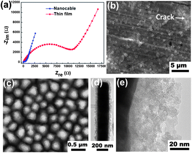 |
| | Fig. 5 (a) Nyquist plots of the Ni–Si nanocable and Si film electrodes at the potential of 2 V during the charging process. Plan-view SEM images of those two electrodes taken after delithiation (b) thin film; (c) nanocable. TEM images taken from the nanocable sample after delithiation (d) low magnification; (e) high magnification. | |
Optimal thickness of the Si shell for better rate performance
With such a promising nanocable array configuration, it is important to determine the optimum Si shell thickness for the best electrochemical performance. Generally speaking, a thinner shell of Si can shorten the transport pathways of ions and electrons, which will enhance the rate performance of the electrode. However, the formation of the SEI layer will consume a certain amount of Si atoms, reducing the actual mass of the active material. This effect is more significant when the Si shell is very thin (Fig. 6a). Therefore, an optimal thickness for the Si shell should be found. To identify the optimum Si shell thickness, we electrodeposited Si on the Ni nanowire arrays with different quantities of charge passed at the electrodes (0.2, 0.4, and 1.0 A s, as shown in Fig. 6b–d). The thickness of the Si shells is 28 ± 3 nm, 42 ± 6 nm, and 81 ± 9 nm, correspondingly. During the electrochemical test, all samples (including the previous sample with a 52 nm Si shell) exhibit similar capacities (∼2000 mA h g−1) at the very low rate of 0.05 C. The rate retention of those nanocable electrodes at various charging rates are shown in Fig. 6e. For all samples, the rate retention drops when the rate is increased. However, when the shell thickness is increased from 28 nm to 52 nm, the capacity retention is improved. As the shell thickness is further increased to 81 nm, the capacity retention declines sharply (especially at high rates). At the rate of 4 C, the capacity retention of this sample is only ∼11%, while the other samples with thinner Si shells remain at ∼30–38%. EIS analysis indicates that the surface resistance rises with the Si shell thickness increase and becomes largest when the thickness of the Si shell reaches 81 nm (Fig. 6f). The high surface resistance and long Li diffusion path length results in the worst rate performance of this thicker sample (81 nm). On the other hand, the adverse effect of the SEI layer is more noticeable for the nanocable electrode with the thinnest Si shell (e.g. 28 nm). As a result, an optimal thickness of the Si shell of ∼52 nm is identified for the present nanocable array electrodes for the best rate performance (Fig. 6e). |
| | Fig. 6 (a) Schematic diagram of the Ni–Si nanocable with different shell thickness. Plan-view SEM images of the electrodeposited Si with different quantities of charge passed through the electrodes (b) 0.2 A s; (c) 0.4 A s; (d) 1.0 A s. (e) Comparison of the capacity retention of the nanocable electrodes deposited with Si shell thickness ranging from 28–81 nm. (f) Nyquist plots of those nanocable electrodes at the potential of 2 V during the charging process. The high-to-medium frequency region is enlarged in the inset. | |
Conclusions
In summary, 3D Ni core–Si shell nanocable array anodes were fabricated by electrodeposition. In this composite configuration, the metallic Ni nanowire arrays act both as a mechanical support and a nanostructural current collector for the electrodeposited active material Si. Moreover, the internal pores of the nanocable array electrodes help to accommodate the large volume change during the lithiation–delithiation process, thus mitigating the internal stress built up. Consequently, the composite nanocable array electrode exhibits a considerable improvement in electrochemical performance when compared to its thin film counterpart of the same mass. It achieves a stable capacity of ∼1900 mA h g−1 at 0.05 C, with ∼1130 mA h g−1 at a higher rate of 1 C (∼2160% improvement compared to that of the thin film) with good capacity retention. Furthermore, an optimal thickness of the Si shell of ∼52 nm is identified for the present nanocable array electrodes with the best rate performance.Acknowledgements
This work is supported by General Research funding of the Research Grants Council under project no. 414612. Y. S. Meng acknowledges the support of the American Chemical Society Petroleum Research Fund (51311-DNI10).Notes and references
- H. Wu and Y. Cui, Nano Today, 2012, 7, 414–429 CrossRef CAS PubMed.
- J. R. Szczech and S. Jin, Energy Environ. Sci., 2011, 4, 56–72 CAS.
- C. K. Chan, H. Peng, G. Liu, K. McIlwrath, X. F. Zhang, R. A. Huggins and Y. Cui, Nat. Nanotechnol., 2008, 3, 31–35 CrossRef CAS PubMed.
- T. Song, J. Xia, J. H. Lee, D. H. Lee, M. S. Kwon, J. M. Choi, J. Wu, S. K. Doo, H. Chang, W. I. Park, D. S. Zang, H. Kim, Y. Huang, K. C. Hwang, J. A. Rogers and U. Paik, Nano Lett., 2010, 10, 1710–1716 CrossRef CAS PubMed.
- M. Ge, J. Rong, X. Fang and C. Zhou, Nano Lett., 2012, 12, 2318–2323 CrossRef CAS PubMed.
- H. Wu, G. Chan, J. W. Choi, I. Ryu, Y. Yao, M. T. McDowell, S. W. Lee, A. Jackson, Y. Yang and L. Hu, Nat. Nanotechnol., 2012, 7, 310–315 CrossRef CAS PubMed.
- S. K. Soni, B. W. Sheldon, X. C. Xiao and A. Tokranov, Scr. Mater., 2011, 64, 307–310 CrossRef CAS PubMed.
- L.-F. Cui, L. Hu, H. Wu, J. W. Choi and Y. Cui, J. Electrochem. Soc., 2011, 158, A592 CrossRef CAS PubMed.
- G. J. Nelson, B. N. Cassenti, A. A. Peracchio and W. K. S. Chiu, J. Electrochem. Soc., 2012, 159, A598–A603 CrossRef CAS PubMed.
- A. Esmanski and G. A. Ozin, Adv. Funct. Mater., 2009, 19, 1999–2010 CrossRef CAS.
- L. Hu, H. Wu, Y. Gao, A. Cao, H. Li, J. McDough, X. Xie, M. Zhou and Y. Cui, Adv. Energy Mater., 2011, 1, 523–527 CrossRef CAS.
- F. F. Cao, J. W. Deng, S. Xin, H. X. Ji, O. G. Schmidt, L. J. Wan and Y. G. Guo, Adv. Mater., 2011, 23, 4415–4420 CrossRef CAS PubMed.
- X. Chen, K. Gerasopoulos, J. Guo, A. Brown, C. Wang, R. Ghodssi and J. N. Culver, Adv. Funct. Mater., 2011, 21, 380–387 CrossRef CAS.
- H. Zhang and P. V. Braun, Nano Lett., 2012, 12, 2778–2783 CrossRef CAS PubMed.
- C. Yu, X. Li, T. Ma, J. Rong, R. Zhang, J. Shaffer, Y. An, Q. Liu, B. Wei and H. Jiang, Adv. Energy Mater., 2012, 2, 68–73 CrossRef CAS.
- X. Chen, K. Gerasopoulos, J. Guo, A. Brown, R. Ghodssi, J. N. Culver and C. Wang, Electrochim. Acta, 2011, 56, 5210–5213 CrossRef CAS PubMed.
- X. Chen, K. Gerasopoulos, J. Guo, A. Brown, C. Wang, R. Ghodssi and J. N. Culver, ACS Nano, 2010, 4, 5366–5372 CrossRef CAS PubMed.
- R. P. U. Karunasiri, R. Bruinsma and J. Rudnick, Phys. Rev. Lett., 1989, 62, 788–791 CrossRef.
- J. Gobet and H. Tannenberger, J. Electrochem. Soc., 1988, 135, 109–112 CrossRef CAS PubMed.
- J. P. Nicholson, J. Electrochem. Soc., 2005, 152, C795–C802 CrossRef CAS PubMed.
- P. L. Taberna, S. Mitra, P. Poizot, P. Simon and J. M. Tarascon, Nat. Mater., 2006, 5, 567–573 CrossRef CAS PubMed.
- T. Munisamy and A. J. Bard, Electrochim. Acta, 2010, 55, 3797–3803 CrossRef CAS PubMed.
- J. W. Choi, J. McDonough, S. Jeong, J. S. Yoo, C. K. Chan and Y. Cui, Nano Lett., 2010, 10, 1409–1413 CrossRef CAS PubMed.
- E. A. Gulbransen and K. F. Andrew, J. Electrochem. Soc., 1954, 101, 128–140 CrossRef CAS PubMed.
- H. J. Mathieu, M. Datta and D. Landolt, J. Vac. Sci. Technol., A, 1985, 3, 331–335 CAS.
- S. Schamm, R. Berjoan and P. Barathieu, Mater. Sci. Eng., B, 2004, 107, 58–65 CrossRef PubMed.
- Z. W. Yuan, S. Csillag, M. A. Tafreshi and C. Colliex, Ultramicroscopy, 1995, 59, 149–157 CrossRef CAS.
- E. Görlich, J. Haber, A. Stoch and J. Stoch, J. Solid State Chem., 1980, 33, 121–124 CrossRef.
- N. Koshizaki, H. Umehara and T. Oyama, Thin Solid Films, 1998, 325, 130–136 CrossRef CAS.
- M. C. Biesinger, B. P. Payne, L. W. M. Lau, A. Gerson and R. S. C. Smart, Surf. Interface Anal., 2009, 41, 324–332 CrossRef CAS.
- J. C. Li, A. K. Dozier, Y. C. Li, F. Q. Yang and Y. T. Cheng, J. Electrochem. Soc., 2011, 158, A689–A694 CrossRef CAS PubMed.
- L. B. Chen, J. Y. Xie, H. C. Yu and T. H. Wang, J. Appl. Electrochem., 2009, 39, 1157–1162 CrossRef CAS.
- C. K. Chan, R. Ruffo, S. S. Hong and Y. Cui, J. Power Sources, 2009, 189, 1132–1140 CrossRef CAS PubMed.
- S. P. V. Nadimpalli, V. A. Sethuraman, S. Dalavi, B. Lucht, M. J. Chon, V. B. Shenoy and P. R. Guduru, J. Power Sources, 2012, 215, 145–151 CrossRef CAS PubMed.
- R. Epur, M. Ramanathan, F. R. Beck, A. Manivannan and P. N. Kumta, Mater. Sci. Eng., B, 2012, 177, 1157–1162 CrossRef PubMed.
- J. W. Wang, Y. He, F. Fan, X. H. Liu, S. Xia, Y. Liu, C. T. Harris, H. Li, J. Y. Huang, S. X. Mao and T. Zhu, Nano Lett., 2013, 13, 709–715 CrossRef CAS PubMed.
- M. T. McDowell, S. W. Lee, J. T. Harris, B. A. Korgel, C. Wang, W. D. Nix and Y. Cui, Nano Lett., 2013, 13, 758–764 CrossRef CAS PubMed.
- N.-S. Choi, K. H. Yew, K. Y. Lee, M. Sung, H. Kim and S.-S. Kim, J. Power Sources, 2006, 161, 1254–1259 CrossRef CAS PubMed.
- V. Etacheri, O. Haik, Y. Goffer, G. A. Roberts, I. C. Stefan, R. Fasching and D. Aurbach, Langmuir, 2011, 28, 965–976 CrossRef PubMed.
- R. Ruffo, S. S. Hong, C. K. Chan, R. A. Huggins and Y. Cui, J. Phys. Chem. C, 2009, 113, 11390–11398 CAS.
- T. S. Arthur, D. J. Bates, N. Cirigliano, D. C. Johnson, P. Malati, J. M. Mosby, E. Perre, M. T. Rawls, A. L. Prieto and B. Dunn, MRS Bull., 2011, 36, 523–531 CrossRef CAS.
- X. H. Liu, S. Huang, S. T. Picraux, J. Li, T. Zhu and J. Y. Huang, Nano Lett., 2011, 11, 3991–3997 CrossRef CAS PubMed.
- S. Misra, N. Liu, J. Nelson, S. S. Hong, Y. Cui and M. F. Toney, ACS Nano, 2012, 6, 5465–5473 CrossRef CAS PubMed.
Footnote |
| † Electronic supplementary information (ESI) available: Characterizations including EDX spectra, energy loss spectra and XPS spectra of the oxidized Si sample. See DOI: 10.1039/c3nr02635c |
|
| This journal is © The Royal Society of Chemistry 2013 |
Click here to see how this site uses Cookies. View our privacy policy here.  Open Access Article
 This Open Access Article is licensed under a Creative Commons Attribution-Non Commercial 3.0 Unported Licence