 Open Access Article
 This Open Access Article is licensed under a
 Creative Commons Attribution 3.0 Unported Licence
Mn12 single molecule magnets deposited on μ-SQUID sensors: the role of interphases and structural modifications†
Elena
Bellido
ab,
Pablo
González-Monje
ab,
Ana
Repollés
c,
Mark
Jenkins
c,
Javier
Sesé
c,
Dietmar
Drung
d,
Thomas
Schurig
d,
Kunio
Awaga
e,
Fernando
Luis
*c and
Daniel
Ruiz-Molina
*ab
aICN2 Institut Catala de Nanociencia i Nanotecnologia, Campus UAB, 08193 Bellaterra (Barcelona), Spain. E-mail: druiz@cin2.es; Fax: +34 935813717
bCSIC - Consejo Superior de Investigaciones Cientificas, ICN2 Building, Campus UAB, 08193 Bellaterra (Barcelona), Spain
cInstituto de Ciencia de Materiales de Aragón, CSIC – Universidad de Zaragoza, 50009 Zaragoza, Spain. E-mail: fluis@unizar.es
dPhysikalisch-Technische Bundesanstalt (PTB), 10587 Berlin, Germany
eResearch Center for Materials Science and Department of Chemistry, Nagoya University, Nagoya 464-8602, Japan
First published on 13th September 2013
Abstract
Direct measurements of the linear ac susceptibility and magnetic relaxation of a few Mn12 monolayers deposited on a μ-SQUID sensor are reported. In order to integrate the molecules into the device, DPN has been the technique of choice. It enabled the structuration of the molecules on the most sensitive areas of the sensor without the need for any previous functionalization of the molecule or the substrate, while controlling the number of molecular units deposited on each array. The measurements reveal that their characteristic SMM behaviour is lost, a fact that is attributed to molecular distortions originated by the strong surface tensions arising at the molecular interphases.
Introduction
Since their discovery in the early 90s,1 single-molecule magnets (SMMs) have aroused interest as an alternative and complementary approach to replace inorganic solids on magnetic devices and applications.2 These molecular clusters show slow magnetic relaxation and magnetization hysteresis3 thanks to the combination of high-spin ground states and strong axial magnetic anisotropy.4 In addition, they also exhibit other interesting phenomena such as quantum tunnelling of the magnetization.5 Advantages of SMMs over their inorganic counterparts are their small size, below a few nanometres, their close to perfect monodispersity, and the fact that they can be obtained in large quantities in a reproducible manner at reasonably low costs and manipulated in a large variety of solvents and matrices. Yet, applications remain elusive. A fundamental issue that still needs to be addressed is the development of strategies for the evolution of bulk materials to nanostructures organized over the surfaces of solid substrates while retaining their characteristic magnetic behaviour.The archetypical case for all these years has been the dodecamanganese acetate cluster (Mn12-ac) and its derivatives.6 The number of successful techniques employed for their structuration on surfaces (with a few exceptions, under vacuum conditions) is considerably large.7 However, preservation of their SMM behaviour still remains a controversial and challenging issue. Other complexes, such as the Fe4 derivatives, provide promising alternatives to circumvent this difficulty.8 Though, the large number of studies aimed to integrate Mn12 on surfaces represents an excellent scenario to discuss some of the main challenges still lying ahead. Such information is crucial for an efficient design of future hybrid devices based on SMMs.
For instance, direct charge transfer to the substrate has been reported as one of the main mechanisms leading to the loss of SMM behaviour, upon chemical modification of the magnetic core. O'Shea et al. have observed a significant charge transfer between gold and a monolayer of Mn12-ac molecules even after protection of the magnetic core with large benzoate ligands.9 Sessoli et al. also observed a partial reduction to Mn(II) on Au(111) for two different Mn12 thio-derivatives.10 More successful were Pennino et al.11 These authors organized monolayers of Mn12 with longer thiol-terminated ligands on Au(111), and found that a large fraction of molecular cores retain their structural integrity. Such divergence of results between different experiments can be attributed to the role that the isolating organic layer plays in decoupling the core magnetic ions from the surface, as recently shown by Forment-Aliaga et al.12 and Voss et al.13 One of the best alternatives to overcome these chemical restrictions is to use substrates with different charge transfer properties. For this, Ternes et al. recently demonstrated the controlled deposition of fragile Mn12 SMMs on thin-insulating surfaces such as boron nitride (BN) and the feasibility for preserving their quantum magnetism.14 Some studies performed with different substrates, such as HOPG,15 glass16 or silicon,17 have also been reported.
Further studies have shown that preserving the core is a necessary but not sufficient condition to retain the SMM relaxation behaviour of Mn12 clusters. Local symmetry changes at the Mn sites, arising from the interplay of attractive and repulsive molecule–surface interactions, can also take place. This has been directly inferred from the modification of the spectral line shape of X-ray absorption spectra (XAS)18 or by atomic force microscopy (AFM) force-volume imaging experiments.19 Such symmetry changes prompted modification of local Jahn–Teller distortions in a rather uncontrolled manner and, therefore, modification of their magnetic relaxation through variations of the magnetic anisotropy constant D.
In any case, testing the magnetic properties of the Mn12 molecules on the surface clearly represents the best alternative approach to assess their behaviour. So far, most of the techniques applied to this end have been based on indirect probes, such as Scanning Tunneling Microscopy (STM), β-detected Nuclear Magnetic Resonance (β-NMR) or mainly X-Ray Magnetic Circular Dichroism (XMCD).10,11,17–20 However, direct measurement of the magnetic properties with a μ-SQUID sensor has remained so far elusive due to the insufficient sensitivity and the lack of experimental techniques for their proper integration. This represents a key challenge in the field nowadays.
In this work, the ac magnetic susceptibility of Mn12 benzoate (Mn12bz) is directly measured by depositing a few layers of the molecular material on the most sensitive areas of a miniaturized Superconducting Quantum Interference Device (μ-SQUID) susceptometer. The frequency-dependent blocking of the ac linear response is one of the characteristic traits of a SMM. A variation of the frequency and temperature over wide ranges enables the exploration of spin relaxation phenomena and provides information on the magnetic energy level schemes. Therefore, the implementation of these devices and their application to the study of molecular nanostructures provides a relatively simple and powerful method for directly characterizing SMMs deposited on a substrate. Integration of the molecules onto the optimum region of the device has been addressed by means of Dip-Pen Nanolithography (DPN). It has already been shown that DPN is an excellent technique to accurately deposit magnetic nanoparticles on a μ-SQUID without the need for any previous functionalization,21 while controlling the number of molecular units deposited on each array.22
Experimental
Materials
Mn12bz was synthesized by following synthetic protocols published previously.23 Glycerol (GC, ≥99%) and N,N-dimethylformamide (DMF, anhydrous, 99.8%) were purchased from Sigma-Aldrich, whereas ethanol absolute (Sps, >99.8%) and acetonitrile (190 Sps, far UV/gradient quality, >99.9%) were purchased from Romil. All these materials were used as received without further purification.Substrates
Silicon bearing native oxide layer (Si/SiO2) substrates were prepared by initially cutting silicon wafers into 0.5 × 0.5 cm2 pieces. Then, each Si/SiO2 substrate was washed in an ultrasonic bath for 10 min with acetonitrile, ethanol, and Milli-Q water and dried by blowing nitrogen gas. Carbon-coated TEM grids, carbon type-B, 200 mesh copper grids were purchased from Ted Pella, Inc.Dip-pen nanolithography experiments
DPN experiments were performed with an Nscriptor™ DPN System (from NanoInk, Inc.). Environmental conditions of ∼40% relative humidity and room temperature were kept constant during all patterning processes with an integrated environmental chamber as part of the Nscriptor DPN System. Tips specially designed for writing purposes were used in all the DPN experiments. Specifically, commercial silicon nitride Type M Probe Arrays and Type A Single Pens (from NanoInk, Inc.) with a spring constant of 0.5 N m−1 and 0.1 N m−1, respectively, were used. To coat the tip, a microfluidic ink delivery chip-based system (Inkwell, from NanoInk, Inc.) was used. The inkwells contain several reservoirs that are filled with the desired ink solution with the help of a micropipette. Afterwards the ink is transferred to the microwells where the tips are dipped for a given time. The excess of ink coating the tip is reduced by bringing the freshly coated tip in contact with a Si/SiO2 substrate and creating spots with an average diameter of several micrometers, which quickly decreased in size. After having deposited a few micrometer-sized spots, it is possible to start writing uniform dots in a very controllable manner. To create patterns over large areas of the Si/SiO2 surface, MP tips were chosen, since once coated they allow creating 12 identical structures in one single step on Si/SiO2. Tips were repeatedly dipped into the reservoirs and used for writing until depletion of the ink, allowing patterning of large arrays over a span of hours.Characterization methods
Dynamic noncontact mode AFM images were recorded on an Agilent 5500 AFM/SPM microscope. For this purpose, noncontact high-resonance frequency with reflex coating (NCHR) tips were used, which are PPP-NCH silicon point probes with a spring constant of ∼42 N m−1 and a resonant frequency of ∼330 kHz (from Nanosensors). AFM image processing and rendering was done with Gwyddion data analysis software. HR-TEM images, EDX analysis and SAED were carried out on a JEM-2100 microscope (from JEOL LTD) with an acceleration voltage of 80 to 200 kV. Additional TEM images were taken with a JEM-1400 microscope (from JEOL LTD) with an acceleration voltage of 40 to 120 kV. Static contact angle measurements, based on the sessile drop method, were performed using a drop shape analyzer Easy Drop combined with Drop Shape Analysis DSA1 (from Kruss). In the experiment a 3 μl droplet of the ink solution was deposited on the target substrate surface using a micropipette. The contact angle was measured on five different regions of the substrate and an average value was obtained from all the measures. SEM images were recorded on a FEI dual beam Helios 600. Grazing incidence XRD measurements were performed on a Panalytical X'Pert Pro X-ray diffractometer by using constant grazing incidence (0.5°) and parallel beam optics. The analysed area was about 5 × 20 mm2. IR spectra were recorded on a TENSORTM 27 FT-IR spectrometer with an ATR accessory from Bruker Optics. XPS experiments were performed using a PHI 5500 Multitechnique System (from Physical Electronics) with a monochromatic X-ray source (Aluminium Kalfa line of 1486.6 eV energy and 350 W), placed perpendicular to the analyzer axis and calibrated using the 3d5/2 line of Ag with a full width at half maximum (FWHM) of 0.8 eV. The area under analysis was a circle of 0.8 mm diameter. The energy resolutions were 187.5 eV of Pass Energy and 0.8 eV per step for the general spectra and 23.5 eV of Pass Energy and 0.1 eV per step for the spectra of the different elements. All XPS measurements were made in an ultra high vacuum (UHV) chamber with pressures between 5 × 10⁻⁹ and 2 × 10⁻⁸ torr.MicroSQUID susceptometer
A new generation of integrated μ-SQUID susceptometers was developed at PTB.24 The devices are made of Nb deposited on Si/SiO2 wafers and they are fabricated by optical lithography. In order to enhance the coupling between the sample and the sensor with respect to that achieved with previous designs,25,26 the diameters of the two circular loops forming the SQUID were reduced to 30 μm. The ac excitation coil allows the application of ac magnetic fields with amplitudes of up to 10 Oe to be compared with amplitudes of approximately 0.1 Oe available with our first and second generation μ-SQUIDs.25,26 In addition, the device was designed with close to perfect reflection symmetry, in order to minimize the output signal when no sample is present. The instrument exhibits a white flux noise of 1.3μΦ0 Hz−1/2.Results
Surface structuration
In a typical DPN experiment, an Atomic Force Microscope (AFM) tip is first functionalized with a solution that contains the molecular entities (referred to as ink). Then, the coated tip is used to directly transfer the ink, in the form of droplets, to the surface. Notwithstanding, the ink solvent plays an important role in the integration process and should fulfil the following characteristics: (i) an adequate viscosity to ensure homogeneous coating of the tip and a controlled transfer of the material; (ii) a high boiling point to maintain the liquid state over the whole writing process (iii) a proper solvent−surface wettability balance to guarantee both the controlled delivery of the ink and the maintenance of the structure once the ink is dried and (iv) a high solubility and stability of Mn12bz.In view of these considerations, our first experiments were devoted to finding a proper solvent for the structuration of Mn12bz on Si/SiO2 substrates. This is the material used in the sensitive μ-SQUID areas. Most of the above described requirements were met by a binary mixture of dimethylformamide (DMF)![[thin space (1/6-em)]](https://www.rsc.org/images/entities/char_2009.gif) :glycerol. DMF exhibits a high boiling point (b.p. 153 °C) and a relatively high viscosity, both enhanced by adding glycerol to the ink solution (b.p. 290 °C). The glycerol ratio was tuned by measuring for different solutions both the contact angle (CA) of the deposited drops, which depends on the electrical polarity of the mixture, and the ability to transfer the solution from the AFM tip to the substrate (viscosity).
:glycerol. DMF exhibits a high boiling point (b.p. 153 °C) and a relatively high viscosity, both enhanced by adding glycerol to the ink solution (b.p. 290 °C). The glycerol ratio was tuned by measuring for different solutions both the contact angle (CA) of the deposited drops, which depends on the electrical polarity of the mixture, and the ability to transfer the solution from the AFM tip to the substrate (viscosity).
CA of μl droplets deposited on Si/SiO2 substrates significantly increases with the glycerol concentration; values of ∼10°, ∼18°, ∼20° and ∼24° were measured for, respectively, pure DMF, and mixtures of DMF + 5% v/v glycerol, DMF + 15% v/v glycerol and DMF + 20% v/v glycerol (see Fig. S1 of the ESI†). A larger CA upon glycerol concentration increase allows for a better control on the resulting morphologies, because it helps maintaining the pattern shape intact during the drying of droplets. However, an increase in the glycerol concentration also induces a considerable increase of the viscosity that disrupts the ink transfer from the AFM tip. Therefore, the optimum DMF:glycerol ratio found, after different deposition experiments, is a compromise between 5 and 10% v/v. The stability of the molecular system in such a binary mixture was confirmed by spectroscopic experiments, more specifically by attenuated total reflectance-Fourier transform infrared spectroscopy (ATR-FTIR) and X-ray photoelectron spectroscopy (XPS) (see ESI, S2 and S3,† respectively).
A dark brown-colored solution of Mn12bz (10–20 mg mL−1) in a DMF:glycerol (95:5) mixture was freshly prepared and used as ink for coating the tip (for more details see the Experimental section). The coated tip was brought into contact with the surface to deposit drops of controlled size. Mn12 arrays can then be fabricated by traversing the tip over the desired area. Reproducible and uniform in size structures were obtained in this way. As a representative example, Fig. 1a shows a well-defined array of Mn12bz made of 20 × 20 dots spaced by 2 μm. The height profile analysis of the dots reveals a high uniformity in size, with an average diameter of 555 ± 39 nm and a height of 6 ± 1 nm. Considering the dimensions expected for the disk-like Mn12bz molecule, of approximately 2.1 × 1.2 nm (obtained by molecular modelling), and taking into account the presence of some residues remaining after solvent evaporation, the height of these dots is in agreement with the distribution of the molecules forming no more that 2–4 molecular layers. To illustrate the effect of the solvent on the final dimensions and structure of the arrays, Fig. 1b shows results obtained, under the same conditions, with a Mn12bz-free mixture of DMF and 5% v/v of glycerol. AFM analysis of the structures indicates a surface topography of up to 1 nm, attributed to the presence of some solvent residues that can be clearly differentiated from our material.
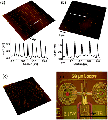 | ||
| Fig. 1 Top: arrays fabricated by DPN on Si/SiO2 substrates. 3-D AFM topography image and height profiles recorded along the white dashed lines in the corresponding AFM images are shown. The specifications for each particular case are: (a) ink composition: Mn12bz (10 mg mL−1) in DMF and 5% v/v of glycerol; (b) ink composition: DMF and 5% v/v of glycerol. Bottom: (c) 3-D AFM topography image of the circular pattern specially designed to fit inside the pickup coil of the susceptometer. The external diameter is 25 μm and the distance between dots is 1 μm. The array was fabricated on Si/SiO2 using the same experimental conditions as in (a). (d) Optical image of the two pickup coils that correspond to the sensitive areas of the microSQUID sensor. The sample to be measured can be located on either the left hand side (A), wherein as an example a sample is indicated with a red circle, or the right hand side (B). | ||
Further control over parameters such as the ink loading of the tip, its movement over the surface and the tip-substrate contact time allowed us to gain control over the deposited structural motifs. As a representative example, Fig. 1c shows a pattern pre-designed to fit inside the internal diameter of the μ-SQUID (27 μm, see Fig. 1d). This pattern consists of concentric circles of dots separated by 1 μm.
Grazing incidence X-ray diffraction (GI-XRD) was used to determine the degree of crystallinity of the deposits. Experiments were performed on two different samples: a thin-film and a structured sample. The thin-film sample was prepared by drop casting Mn12bz ink on a substrate, while the structured sample was fabricated by DPN. For the latter, the size of the droplets was adjusted to ∼1 μm and the deposition process was repeated over extended areas in order to cover up to a few square millimetres, which are required to have enough sensitivity with this experimental technique (see ESI, S4–S5†).
The absence of any clear diffraction peak at low 2θ angles indicates that both samples are amorphous or that they possess a very small degree of crystallinity (see Experimental section). It could also be possible, especially in the case of the structured samples (arrays), that the signal is too small to be detected by the present XRD setup. Further evidence for the amorphous nature of Mn12bz deposits was obtained by high-resolution transmission electron microscopy (HR-TEM) experiments. It should be noted that HR-TEM images were taken with a minimum electron dose, in order to avoid damaging the sample with the beam. Typical HR-TEM images of the arrays are shown in Fig. 2. Even though several dots were inspected over a range of samples, no lattice fringes were observed in any of them (Fig. 2c, inset). These results suggest that Mn12bz droplets deposited on surfaces and exposed to ambient conditions tend to dry as an amorphous material. This is further supported by the presence of a diffuse halo in the selected area electron diffraction (SAED) patterns obtained from regions inside all dots under study (see Fig. 2d).
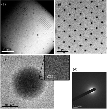 | ||
| Fig. 2 HR-TEM images of (a) three different arrays of Mn12bz fabricated on a carbon-coated TEM grid and (b) magnification view of one of the arrays. Ink composition: Mn12bz (10 mg mL−1) in DMF and 5% v/v of glycerol. (c) Details of one of the dots of the array. (The inset shows the magnification view of a region inside the dot). (d) Electron diffraction pattern obtained from a region inside the dot. | ||
Integration of molecular samples into μ-SQUID sensors
The μ-SQUID susceptometer used for these studies24 consists of the μ-SQUID sensor itself and an ac excitation coil, which generates a close to uniform magnetic field 0.01 Oe < hac < 7 Oe oscillating with time at frequency ω. As Fig. 1d shows, the μ-SQUID has a gradiometric design, with two circular loops wound in opposite directions and linked together by two Josephson junctions. The sensor converts the net magnetic flux through these two coils, which arises from any imbalance between the flux “seen” by each of them, into an output voltage. An ac output voltage can therefore be induced by placing a magnetic sample into one of these coils, and applying an ac magnetic field hac. The areas delimited by the two SQUID coils represent the sensitive, or active, areas of the susceptometer. A small, but unavoidable, imbalance between the two coils gives also rise to a finite output signal for the empty susceptometer. This contribution has been measured independently and can be subtracted from the total output signal, in order to obtain the susceptibility of the sample. Yet, this effect limits the minimum detectable voltage to approximately 10−6 V, as it sets a minimum scale for the lock-in amplifier that is used to read-out the SQUID. Under these conditions, it is crucial to optimize the flux coupling of the sample with the SQUID, as this coupling determines the output signal generated by a given sample. This goal is achieved by uniformly depositing the sample inside the coil. For the measurements on Mn12bz samples, we made use of two devices with the same design but with slightly different background signals. We shall refer to them in what follows as SQUID1 and SQUID2.The two Nb coils forming the SQUID are circular-shaped with external and internal diameters of 35 μm and 27 μm, respectively (see Fig. 3). The coil wire has a cross-section of approximately 5 μm × 450 nm (a more detailed description of the sensor is provided in the ESI†). Five different Mn12bz samples were integrated into one of the μ-SQUID coils. Three of these samples were integrated by DPN, as described below, using the experimental conditions already optimized for the controlled deposition of Mn12bz on bare Si/SiO2 (a mixture of DMF and 5% v/v of glycerol). In addition, two “bulk-like” samples were also measured, for comparison purposes, under the same conditions. The first of these consisted of a micron-sized crystal of Mn12bz placed directly onto the coil (B1). The last sample (B2) was microcrystalline powder obtained after evaporation of a DMF solution of the Mn12bz. These two samples were embedded in apiezon-N grease and placed onto the μ-SQUID with the use of a home-made micromanipulator.
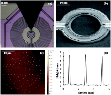 | ||
| Fig. 3 (a) Optical image of the μ-SQUID susceptometer right after the deposition process (b) FE-SEM images taken at 45° tilt angle on one of the susceptometer's pick-up coils after integration of sample DPN1. (c) AFM topography image of a similar array fabricated on Si/SiO2 using the same experimental conditions used for DPN1. (d) Height profile measured by scanning the tip along the black dashed line in image (c). | ||
The first DPN sample (hereafter referred to as DPN1) consisted of a circular pattern of dots deposited inside the μ-SQUID coil of the SQUID1 sensor (see Fig. 3b and c) after completely removing the excess ink at the tip. In order to do so, several spots were fabricated by the freshly coated tip on an auxiliary Si/SiO2 surface until writing uniform dots in a very controllable manner (see Experimental section).
Afterwards, the tip was placed on top of the coil wire to create a circular pattern while keeping the tip-substrate contact time at 0.1 s. The process was repeated 2.5 times to deposit 1320 identical dots inside the coil. After the deposition, the sensor was characterized by scanning electron microscopy (SEM). The images show the effective and regular deposition of the molecular material inside the circular sensing area of the susceptometer (see Fig. 3b). The topography of the array was investigated by performing AFM on a replica fabricated on a bare Si/SiO2 surface (Fig. 3c).
The purpose of this method is to avoid damaging the sensor in the course of the AFM experiments. The analysis of the height profiles, shown in Fig. 3d, reveals the formation of highly uniform in size dots, with an average diameter of 249 ± 9 nm and a height of 8 ± 1 nm. These data suggest that each dot consists of approximately 3–5 Mn12bz layers. Taking into account the size and number of the dots deposited, it can be estimated that about 9.0 × 10⁷ Mn12bz molecules were integrated inside the sensing area of the susceptometer (for more details on the determination of the number of molecules deposited see the ESI†).
In the subsequent deposition of sample DPN2 on sensor SQUID2, the amount of Mn12bz transferred to the device was increased by controlling the amount of ink removed from the tip in the previous step. For this, the freshly coated tip was brought into contact with the auxiliary Si/SiO2 surface for a shorter time than in the previous experiment. Afterwards, the tip was again positioned on the wire of one of the pickup coils by optical control and traversed over the surface, as before, forming a circular pattern with a tip-substrate contact time of 0.1 s.
In this case, the larger volume of the droplets makes them merge together on the substrate, forming a continuous thin film that covers the entire coil (sample DPN2). An optical image of the pickup coil captured during the deposition process is shown in Fig. 4a. The height profile of a replica fabricated under identical conditions but on a bare Si/SiO2 surface indicates a height of ∼8 nm (Fig. 4b). This profile is in agreement with that expected from a Mn12bz multilayer formed by 3–5 molecular layers. The number of molecules deposited on the sensing area is estimated to be of the order of 7.2 × 10⁸ (see ESI†).
 | ||
| Fig. 4 (a) Optical image of the μ-SQUID susceptometer taken after depositing sample DPN2. (b) AFM topography image of a deposit formed on Si/SiO2 under identical conditions to those used for sample DPN2 and (inset) cross-section recorded along the white dashed line in image (b). | ||
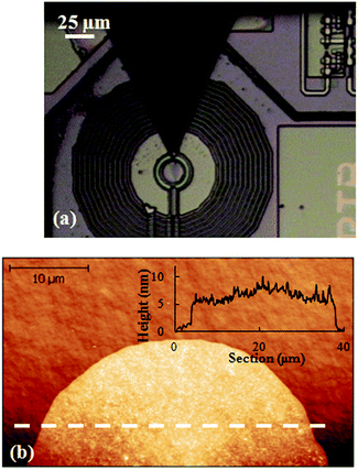
Finally, when the same circular pattern is repeated without previously removing any excess ink from the tip, a large droplet completely covering the coil area with the Mn12bz ink is obtained (sample DPN3). For this, the tip was positioned on the centre of the coil of SQUID1 by optical control and brought into contact with the surface to deliver a sufficient amount of ink in a single step. An image of this “bulky” sample as it looked right after the DPN deposition process is shown in Fig. 5. The topography of the dry droplet was measured by AFM on a similar sample fabricated under identical conditions but on a bare Si/SiO2 surface. The topographic profile shows an average height of ∼15–20 nm, in agreement with the distribution of the molecules into up to 6–8 molecular layers.
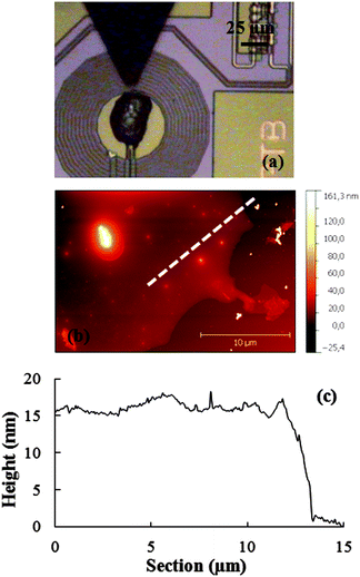 | ||
| Fig. 5 Deposition of a continuous Mn12bz thin-film covering the whole coil area (sample DPN3). (a) Optical image taken during the integration process. (b) AFM topography image of the replica sample fabricated, under the same conditions as in (a), onto a broken μSQUID susceptometer. (d) Height profile measured along the white dashed line in (b). | ||
Magnetic susceptibility measurements
Fig. 6 shows the output signals recorded, at T = 4.2 K and with the μ-SQUID susceptometer SQUID1, from samples B1-2, DPN1 and DPN3. Data measured for sample DPN2 using SQUID2 are given as part of the ESI (Fig. S7†). The response of the crystalline sample (B1) shows the existence of two relaxation processes. The frequency-dependent contribution observed at low frequencies (∼50 Hz) is associated with relaxation of standard (or “slow”) Mn12bz clusters while the second one (∼300 kHz) comes from “fast” relaxing clusters, which represent the majority in this compound.23 The very different relaxation rates observed at T = 4.2 K are in agreement with the different activation energies involved in the spin reversal of these isomers. Similar results were obtained for sample B2 (Fig. 6A and B); the two magnetic relaxation processes remain, that is, Mn12bz clusters largely preserve their magnetic memory. However, the imaginary susceptibility peaks of sample B2, thus also the steps shown by the in phase component, are considerably broader than those of the single crystal, thus suggesting the presence of larger dispersions of relaxation times for both isomers. This is understandable, as the fast recrystallization experienced by sample B2 is bound to increase the density of lattice defects and therefore leads to distribution of molecular environments.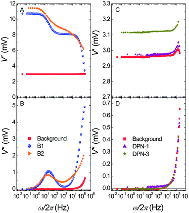 | ||
| Fig. 6 Output signals measured on empty μ-SQUID susceptometer SQUID1 (background) and on the same device after the deposition of several Mn12bz samples. Top: in-phase components. Bottom: out-of-phase components. | ||
The responses of two samples deposited by DPN (DPN-1 and DPN-3) are shown in Fig. 6C and D. The dependence of V′ and V′′ on the frequency differs strikingly from that found for the precursor crystalline material B1. In particular, V′ is close to constant above the background signal of the empty susceptometer, while the imaginary component V′′ vanishes. The same behavior is observed for sample DPN2 (see Fig. S7 of the ESI†).
The upturns observed above 104 Hz can be fully ascribed to the background signal of the μ-SQUID susceptometer. These results show that Mn12bz molecular nanomagnets deposited on silicon substrates remain in equilibrium up to very high frequencies, that is, their magnetic relaxation times become much faster than those in the bulk. It is worth noting that the enhanced magnetic relaxation is not associated with conversion of “slow” into “fast” ones. Instead, the susceptibility data show that drastic changes in the magnetic relaxation mechanisms occur for both isomers.
Before trying to discuss their physical significance, it is important to first make sure that these signals come indeed from the molecular samples. In order to check this question, we have computed, using the commercial simulation software COMSOL, the magnetic flux that an ensemble of Mn12bz molecules couples with one of the μ-SQUID pick-up coils. The model used for these calculations is schematically depicted in Fig. 7A that shows also the spatial distribution of the magnetic field derived from these calculations. The sample is a homogeneous disk, with a density equal to that of Mn12bz but with magnetic easy axes oriented at random, located inside one of the pick-up coils and subjected to the same magnetic field hac = 25 mOe as that used in the experiments. The number of molecules (N) is varied by changing the height h of the disk. For low N (<109), simulations performed on different sample geometries, e.g. on samples formed by discrete dots, give results that are in 30% agreement with those obtained for a continuous disk. Therefore, we conclude that approximating the sample with a continuous disk must be valid for the range of N values that we consider here.
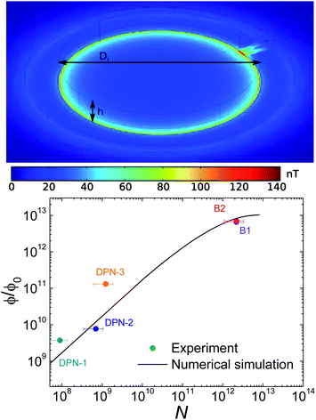 | ||
| Fig. 7 Top: theoretical color plot of the magnetic field intensity generated by a homogeneously magnetized cylinder (height h, diameter Di = 26 μm) located inside one of the μ-SQUID pick-up coils (thin black lines). These numerical calculations are used to determine the magnetic flux ϕ coupled with the device. Bottom: dependence of ϕ as a function of the number of Mn12bz molecules deposited on one of the pick-up coils. The solid line is calculated using the theoretical model described above and varying h between 8 nm (N = 109) and 80 mm (N = 1013). The prediction for N < 109 is a linear extrapolation of these results. | ||
The dependence of the equilibrium magnetic signal on N is shown in Fig. 7. The data are taken from the low-ω limits of frequency-dependent measurements, whereas the solid line represents the results of the above model calculations. In these calculations, the equilibrium susceptibility of each molecule is calculated as χT = g2μB2S2/3kBT, with g = 2 and S = 10. Considering the experimental uncertainties, calculations reproduce very well the measured values. Then, it can be safely concluded that the output signals we measured correspond to the magnetic response of the molecules deposited by DPN. The fact that the equilibrium susceptibility does not change much with respect to that expected for Mn12bz suggests also that the molecular magnetic moments (thus g and S) are preserved.
Discussion
Suitable experimental conditions for the DPN deposition of Mn12bz molecules on Si/SiO2 substrates have been established. Surface characterization techniques show that the molecules retain their structural identity and that there is no significant charge transfer from the surface to the molecules, as previously observed for other Mn12 derivatives deposited on SiO2.27 This has enabled us to integrate such SMMs on the sensitive areas of a μ-SQUID sensor and to directly measure their magnetic relaxation. These measurements reveal that the magnetization relaxation differs from that observed for the bulk material. Similar results were previously observed for a monolayer of Mn12 on silicon (Si) studied using a complementary technique such as β-NMR.28 Since charge transfer effects and/or chemical degradation upon surface deposition can be discarded, environment effects must be considered for a cautious analysis of the drastic changes in spin dynamics. Among them are (I) crystal lattice modifications, i.e. modifications in the acoustic phonon spectrum and/or (II) confinement effects upon nanostructuration. Both possibilities are analyzed in more detail in what follows.(I) Crystal lattice modifications
Modification of spin-phonon relaxation mechanisms may arise from changes in the medium stiffness and density with respect to the bulk sample induced by the amorphous character of the DPN deposits and/or possible solvate molecule remnants.29 However, previously reported Mn12 bulk studies discard this possibility. Indeed, studies performed under two extreme conditions (a crystalline sample and a nearly amorphous material) have shown that long-range crystalline disorder affects little the anisotropy, magnetic relaxation, and magnetic quantum tunneling of these materials.30 In fact, amorphous Mn12-based sub-50 nm spherical particles have been shown to retain the SMM behaviour with an activation energy U = 63(1) K, which is close to the value of U = 65(1) K found in bulk crystals. In both studies, only a subtle influence was detected; the faster tunneling rates measured for the amorphous material can be accounted for by changes in the distribution of dipolar bias and/or by an increase of the density of available vibrations with respect to an ordered solid. These results are not surprising, since previous studies on Mn12 molecules in frozen solutions31 and polymeric dispersions32 already showed a lowering of the magnetization relaxation but never justified the complete disappearance of the SMM behaviour. Finally, experiments performed on recrystallized sample B2 show also minor quantitative changes in the frequency-dependent response (see Fig. 6). Therefore, tentatively we discard acoustic phonon modifications or, in general, the lack of crystalline order, as the dominant physical cause responsible for the loss of SMM behaviour in our Mn12 deposits.(II) Confinement effects upon nanostructuration
Surface effects on the magnetization relaxation of Mn12 SMMs upon surface deposition have already been studied.33,10 This is most likely our case due to the strong interaction of the first molecular layer with the surface and/or molecular strengths appearing at the outmost solid–air interphase. Such interactions prompted modulation of the molecular mechanical properties through structural modifications, as has recently shown by force-volume imaging experiments.19 This in turn will modify the axial anisotropy parameter (D) and their magnetization relaxation properties. Moreover, not only D but also other parameters such as the second-order transverse anisotropy terms (E) have been shown to be influenced. For instance, a recent study showed that the spin reversal time of standard Mn12bz clusters decreases by 13% on reducing the crystal size from 11.5 to 0.4 μm (while maintaining constantly the same crystalline phase). The observed decrease in the effective energy barrier was associated with the existence of a distribution of E parameters, centred at E = 0, which broadens as the crystal size decreases and the surface/volume ratio of the particles increases.34 While such effects are neither dominant in a crystal35 nor in thick films deposited by different lithographic techniques,36 in the case of deposition of a few layers they turn out to be crucial.Conclusions
AFM-based lithography has been shown to be a suitable technique for the controlled integration of SMMs on magnetic sensors. The archetypal Mn12bz system has been selectively deposited on a μ-SQUID sensor allowing for the first time the direct measurement of the frequency-dependent dynamical ac susceptibility of a few SMM layers. The results evidence the loss of the characteristic SMM behaviour, putting into evidence the relevance of nanoscale surface constraint effects when dealing with a few layers thick molecular film. Any future practical application out of SMMs will require overcoming these limitations by the use of more robust SMMs,37 but more importantly, by preventing any modification that results from their deposition on surfaces.Acknowledgements
This work was partly funded through grants MAT2012-38318-C03 of Spanish MINECO and MOLCHIP from Gobierno de Aragón. E.B. thanks the MICINN for a predoctoral grant. We would like to thank Red de Bibliotecas del CSIC for their support to publish this work in open format.Notes and references
- R. Sessoli, D. Gatteschi, A. Caneschi and M. A. Novak, Nature, 1993, 365, 141–143 CrossRef CAS
; R. Sessoli, H. L. Tsai, A. R. Schake, S. Wang, J. B. Vincent, K. Folting, D. Gatteschi, G. Christou and D. N. Hendrickson, J. Am. Chem. Soc., 1993, 115, 1804–1816 CrossRef
-
Magnetochemistry, ed. R. D. L. Carlin, Springer-Verlag, Berlin, 1986 Search PubMed
- J. Gomez-Segura, J. Veciana and D. Ruiz-Molina, Chem. Commun., 2007, 3699–3707 RSC
-
Molecular Nanomagnets, ed. D. Gatteschi, R. Sessoli and J. Villain, Oxford University Press, Oxford, UK, 2006 Search PubMed
- J. R. Friedman, M. P. Sarachik, J. Tejada and R. Ziolo, Phys. Rev. Lett., 1996, 76, 3830–3833 CrossRef CAS
- D. Gatteschi and R. Sessoli, Angew. Chem., Int. Ed., 2003, 42, 268–297 CrossRef CAS PubMed
- N. Domingo, E. Bellido and D. Ruiz-Molina, Chem. Soc. Rev., 2012, 41, 258–302 RSC
- M. Mannini, F. Pineider, P. Sainctavit, C. Danieli, E. Otero, C. Sciancalepore, A. M. talarisco, M.-A. Arrio, A. cornia, D. Gatteschi and R. sessoli, Nat. Mater., 2009, 8, 194–197 CrossRef CAS PubMed
- A. Saywell, A. J. Britton, N. Taleb, M. del Carmen Giménez-López, N. R. Champness, P. H. Beton and J. N. O'Shea, Nanotechnology, 2011, 22, 075704 CrossRef PubMed
- M. Mannini, Ph. Sainctavit, R. Sessoli, Ch. Cartier dit Moulin, F. Pineider, M.-A. Arrio, A. Cornia and D. Gatteschi, Chem.–Eur. J., 2008, 14, 7530–7535 CrossRef CAS PubMed
- U. del Pennino, V. De Renzi, R. Biagi, V. Corradini, L. Zobbi, A. Cornia, D. Gatteschi, F. Bondino, E. Magnano, M. Zangrando, M. Zacchigna, A. Lichtenstein and D. W. Boukhvalov, Surf. Sci., 2006, 600, 4185–4189 CrossRef CAS PubMed
- F. Moro, R. Biagi, V. Corradini, M. Evangelisti, A. Gambardella, V. De Renzi, U. del Pennino, E. Coronado, A. Forment-Aliaga and F. M. Romero, J. Phys. Chem. C, 2012, 116, 14936–14942 CAS
- S. Voss, M. Fonin, U. Rüdiger, M. Burgert, U. Groth and Y. S. Dedkov, Phys. Rev. B: Condens. Matter Mater. Phys., 2007, 75, 045102 CrossRef CAS
- S. Kahle, Z. Deng, N. Malinowski, Ch. Tonnoir, A. Forment-Aliaga, N. Thontasen, G. Rinke, D. Le, V. Turkowski, T. S. Rahman, S. Rauschenbach, M. Ternes and K. Kern, Nano Lett., 2012, 12, 518–521 CrossRef CAS PubMed
- L. Menga, B.-F. Lin, J.-Y. Yang, Y. Sun, R.-F. Dou, L.-X. Mab, Ch. M. Xiong and J.-C. Nie, Chem. Phys. Lett., 2012, 542, 81–84 CrossRef PubMed
- H. Sun, W. Li, L. Wollenberg, B. Li, L. Wu, F. Li and L. Xu, J. Phys. Chem. B, 2009, 113, 14674–14680 CrossRef CAS PubMed
- B. Fleury, V. Huc, L. Catala, P. Jegou, L. Baraton, Ch. David, S. Palacin and T. Mallah, CrystEngComm, 2009, 11, 2192–2197 RSC
- F. Moro, V. Corradini, M. Evangelisti, R. Biagi, V. De Renzi, U. del Pennino, J. C. Cezar, R. Inglis, C. J. Miliosef and E. K. Brechin, Nanoscale, 2010, 2, 2698–2703 RSC
- G. Otero, E. Evangelio, C. Rogero, L. Vázquez, J. Gómez-Segura, J. A. Martín Gago and D. Ruiz-Molina, Langmuir, 2009, 25, 10107–10115 CrossRef CAS PubMed
- M. Mannini,
et al.
, Adv. Mater., 2009, 21, 167 CrossRef CAS
- M. J. Martínez-Pérez, E. Bellido, R. de Miguel, J. Sesé, A. Lostao, C. Gómez-Moreno, D. Drung, T. Schurig, D. Ruiz-Molina and F. Luis, Appl. Phys. Lett., 2011, 99, 032504 CrossRef CAS
- E. Bellido, R. de Miguel, D. Ruiz-Molina, A. Lostao and D. Maspoch, Adv. Mater., 2010, 22, 352–355 CrossRef CAS PubMed
- K. Takeda, K. Awaga, T. Inabe, A. Yamaguchi, H. Ishimoto, T. Tomita, H. Mitamura, T. Goto, N. Mori and H. Nojiri, Phys. Rev. B: Condens. Matter Mater. Phys., 2002, 65, 094424 CrossRef
- S. Bechstein, A. Kirste, D. Drung, M. Regin, O. Kazakova, J. Gallop, L. Hao, D. Cox and T. Schurig, IEEE Trans. Appl. Supercond., 2013, 23, 1602004 CrossRef
- M. J. Martínez-Pérez, J. Sesé, F. Luis, D. Drung and T. Schurig, Rev. Sci. Instrum., 2010, 81, 016108 CrossRef PubMed
- M. J. Martínez-Pérez, J. Sesé, F. Luis, R. Córdoba, D. Drung, T. Schurig, E. Bellido, R. de Miguel, C. Gómez-Moreno, A. Lostao and D. Ruiz-Molina, IEEE Trans. Appl. Supercond., 2011, 21, 345 CrossRef
- R. V. Martínez, F. García, R. García, E. Coronado, A. Forment-Aliaga, F. M. Romero and S. Tatay, Adv. Mater., 2007, 19, 291–295 CrossRef CAS
- Z. Salman, K. H. Chow, R. I. Miller, A. Morello, T. J. Parolin, M. D. Hossain, T. A. Keeler, C. D. P. Levy, W. A. MacFarlane, G. D. Morris, H. Saadaoui, D. Wang, R. Sessoli, G. G. Condorelli and R. F. Kiefl, Nano Lett., 2007, 7, 1551–1555 CrossRef CAS PubMed
- A. R. Farrell, J. A. Coome, M. R. Probert, A. E. Goeta, J. A. K. Howard, M.-H. Lemée-Cailleau, S. Parsons and M. Murrie, CrystEngComm, 2013, 15, 3423–3429 RSC
- C. Carbonera, F. Luis, J. Campo, J. Sánchez-Marcos, A. Camón, J. Chaboy, D. Ruiz-Molina, I. Imaz, J. van Slageren, S. Dengler and M. González, Phys. Rev. B: Condens. Matter Mater. Phys., 2010, 81, 014427 CrossRef
- A. Caneschi, T. Ohm, C. Paulsen, C. Sangregorio and R. Sessoli, J. Magn. Magn. Mater., 1998, 177–181, 1330 CrossRef CAS
- F. El Hallak, J. van Slageren, J. Gómez-Segura, D. Ruiz-Molina and M. Dressel, Phys. Rev. B: Condens. Matter Mater. Phys., 2007, 75, 104403 CrossRef
- L. Bogani, L. Cavigli, M. Gurioli, R. L. Novak, M. Mannini, A. Caneschi, F. Pineider, R. Sessoli, M. Clemente-León, E. Coronado, A. Cornia and D. Gatteschi, Adv. Mater., 2007, 19, 3906–3911 CrossRef CAS
- N. Domingo, F. Luis, M. Nakano, M. Muntó, J. Gómez, J. Chaboy, N. Ventosa, J. Campo, J. Veciana and D. Ruiz-Molina, Phys. Rev. B: Condens. Matter Mater. Phys., 2009, 79, 214404 CrossRef CAS
- L. Chen, W. Wernsdorfer, Ch. Lampropoulos, G. Christou and I. Chiorescu, Nanotechnology, 2010, 21, 405504 CrossRef PubMed
- K. Kim, D. M. Seo, J. Means, V. Meenakshi, W. Teizer, H. Zhao and K. R. Dunbar, Appl. Phys. Lett., 2004, 85, 3872–3874 CrossRef CAS
- M. Mannini, F. Pineider, C. Danieli, F. Totti, L. Sorace, Ph. Sainctavit, M.-A. Arrio, E. Otero, L. Joly, J. C. Cezar, A. Cornia and R. Sessoli, Nature, 2010, 46(8), 417–421 CrossRef PubMed
Footnote |
| † Electronic supplementary information (ESI) available. See DOI: 10.1039/c3nr02359a |
| This journal is © The Royal Society of Chemistry 2013 |