 Open Access Article
 This Open Access Article is licensed under a
 Creative Commons Attribution 3.0 Unported Licence
Incorporation of small BN domains in graphene during CVD using methane, boric acid and nitrogen gas
George
Bepete
ab,
Damien
Voiry
c,
Manish
Chhowalla
c,
Zivayi
Chiguvare†
b and
Neil J.
Coville
*a
aDST/NRF Centre of Excellence in Strong Materials and Molecular Sciences Institute, School of Chemistry, University of the Witwatersrand, WITS 2050, Johannesburg, South Africa. E-mail: neil.covile@wits.ac.za; Fax: +27 11 717 6749
bDST/NRF Centre of Excellence in Strong Materials and Material Physics Research Institute, School of Physics, University of the Witwatersrand, WITS 2050, Johannesburg, South Africa
cMaterials Science and Engineering, Rutgers University, 607 Taylor Road, Piscataway, New Jersey 08854, USA
First published on 29th May 2013
Abstract
Chemical doping of graphene with small boron nitride (BN) domains has been shown to be an effective way of permanently modulating the electronic properties in graphene. Herein we show a facile method of growing large area graphene doped with small BN domains on copper foils using a single step CVD route with methane, boric acid powder and nitrogen gas as the carbon, boron and nitrogen sources respectively. This facile and safe process avoids the use of boranes and ammonia. Optical microscopy confirmed that continuous films were grown and Raman spectroscopy confirmed changes in the electronic structure of the grown BN doped graphene. Using XPS studies we find that both B and N can be substituted into the graphene structure in the form of small BN domains to give a B–N–C system. A novel structure for the BN doped graphene is proposed.
1 Introduction
Since the discovery of atomically thick graphene in 2004,1 it has been considered as one of the most promising candidates for future electronic devices due to its excellent electronic properties2,3 and versatile application possibilities in transparent electronics.4–7 The absence of a band gap in graphene however limits its properties for application in electronic devices and reproducible practical procedures that open a band gap in graphene would widen its applicability. One way of achieving this is by doping.8 Different methods to make doped graphene can introduce these modifications and tune the properties of graphene to render graphene a highly customizable material as has been achieved with carbon nanotubes.9 Making graphene a hole conductor involves the use of electron withdrawing dopants, whilst electron donating dopants are used to make it an electron conductor. Two types of graphene doping have been widely investigated, namely surface transfer doping10 and chemical doping.11 Doping has been achieved by the use of chemical species or an electric field.12 The surface transfer doping methods have been used successfully to modify charge carriers in graphene but the shortcoming of the approach is that the doping is temporary and the doped graphene is difficult to integrate into functional devices. Permanent doping has been achieved in graphene by chemical doping using B for p-type graphene and N for n-type graphene.13 A wide range of precursor materials have been reported to incorporate nitrogen or boron into graphene.14–17Several theoretical studies have shown that simultaneous incorporation of B and N in graphene is thermodynamically possible yielding small planar hexagonal boron nitride (h-BN) domains in graphene and most importantly that this process achieves band gap modulation in graphene.18,19 The band gap opening in graphene, due to doping with small BN domains, has been attributed to the breaking of localized symmetry.20 The tunable electronic properties of graphene material containing BN make this material likely to be useful in electronic devices, composites, energy conversion and storage.21 Indeed, a CVD method has recently been used to grow BN doped graphene on a copper foil using Ar/H2, methane and ammonia borane gases.22 This method produced graphene domains alloyed with discrete large BN domains.
Here we demonstrate a facile, safe process for the chemical vapor deposition synthesis of BN doped graphene on copper using methane, boric acid powder and nitrogen gas. We show that B and N are incorporated and that the N is bonded with the carbon within the graphene structure to make a continuous BN graphene material. Small units of BN in graphene, i.e. one B surrounded by three N and singly occurring hexagonal BN rings containing three B atoms and six N atoms are formed. Three of the N atoms in the hexagonal rings are also bonded to the carbon of the graphene. We provide a simple reproducible experimental method to synthesize large area graphene doped with small BN domains which can be used to make high quality BN doped graphene for possible applications in nanoelectronic devices.
2 Experimental section
2.1 Materials
BN doped graphene was synthesized by a chemical vapor deposition (CVD) method. Copper foil (25 μm thick, Alpha Aesar) was used as the catalyst in this study.23 A 1 cm × 2 cm copper foil was inserted into the centre of a cylindrical quartz tube reactor (22 cm × 100 cm). A copper envelope containing 300 mg boric acid powder was inserted into the quartz tube reactor 4 cm behind the copper foil as shown in Fig. 1. The reactor was evacuated to 30 Torr. A 7% H2 in N2 (H2–N2) gas mixture (Air Gas, batch analyzed grade) was introduced into the reactor at 80 sccm whilst the vacuum was kept at 30 Torr for a further 15 minutes. The reactor was then heated to 995 °C under vacuum. The reactor was held at 995 °C for a further 30 minutes after which methane gas (Air products, Ultrahigh purity) was also introduced at 20 sccm. The reaction was allowed to proceed for 20 minutes. The methane flow was stopped and the reactor was cooled under the H2–N2 gas at 80 sccm. Numerous experiments were conducted to optimize the separation between the boric acid container and the copper foil catalyst. The 4 cm separation distance was found to be the optimal distance for quality graphene growth to take place in the presence of a boric acid source. Methane (20 sccm) and H2–N2 gas (80 sccm) without boric acid was also used to produce undoped graphene using the same procedure. The graphene was transferred onto a silicon substrate with a 300 nm silicon oxide layer (SiO2/Si) as reported in ref. 23. In summary, 5 mm × 5 mm copper foil squares were cut from the 1 cm × 2 cm copper foil catalyst used and poly(methyl methacrylate) (PMMA) (Mico Chem) was spin coated onto the surface of the copper square on a spin coater (3000 rpm). The copper was then etched away from the doped graphene/PMMA layers (3 hours) in a 1 M solution of FeCl3 contained in a Petri dish. After all the copper had been etched away, the graphene/PMMA was left floating in the FeCl3 solution and was then washed several times in a 1 M solution of HCl, followed by washing in water. Lastly the graphene/PMMA was attached to a cleaned SiO2/Si substrate and was left to dry for 2 hours in air at ambient temperature. The PMMA was removed from the graphene by dissolving the PMMA in acetone. This was achieved by placing the PMMA/graphene on the SiO2/Si in a Petri dish containing acetone which was left standing for 15 minutes. The acetone was decanted and replaced by fresh acetone, and the process was repeated 3 times. Lastly the graphene was washed in methanol (to ensure complete removal of PMMA/acetone residues) and left to dry in air under ambient conditions.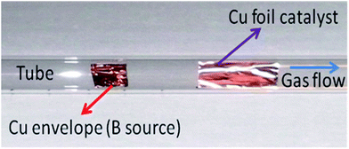 | ||
| Fig. 1 Cylindrical quartz tube reactor showing the inserted copper envelope containing boric acid (boron source) placed 4 cm before the flat copper foil catalyst used for graphene growth. | ||
2.2 Characterization
The doped and undoped graphene samples were characterized on SiO2/Si substrates unless otherwise stated. Optical images of the graphene were recorded using an optical microscope. Surface morphology and graphene thickness characterization studies were conducted by tapping-mode atomic force microscopy (AFM) using a Dimension 3100 from Veeco. Morphological characterization of the BN doped graphene was carried out on graphene transferred onto plain copper grids using a Technai G2 spirit TEM at 120 kV. Raman spectra were measured on an InVia Raman microscope (Reinshaw) at an excitation wavelength of 514 nm. X-ray photoelectron spectroscopy (XPS) measurements were performed with a Thermo Scientific K-Alpha spectrometer. All spectra were recorded using an Al Kα microfocussed monochromatized source (1486.6 eV) with a resolution of 0.6 eV. The spot size was 400 μm and the operating pressure was 5 × 10⁻⁹ Pa.3 Results and discussion
Fig. 2a shows the optical image of the pristine graphene and Fig. 2b shows the optical image of BN doped graphene that was transferred onto SiO2/Si substrates. The images of both the undoped and the BN doped graphene reveal a large area, uniform and continuous material. The pristine graphene in Fig. 2a has a light pink colour while the BN doped graphene (Fig. 2b) is dark pink in colour. The colour contrast suggests that the BN doped graphene could be a single or double layer graphene. Fig. 2c and d show TEM images of a continuous BN doped graphene material on a plain Cu grid. The small dark spots observed are due to residual Cu particles; the holes are due to imperfections in the graphene layer which develop during the transfer process. AFM imaging data revealed a continuous film of BN doped graphene with wrinkles (Fig. 2e) which resulted from the transfer process of the graphene onto the SiO2/Si substrate. The section analysis of the BN doped graphene shown in Fig. 2e revealed a uniform material with a thickness between 1.0 and 1.4 nm indicating that the material was at most a double layer graphene.24 In summary, both AFM and TEM analyses indicate that the BN doped graphene is uniform and of large area (Fig. 2).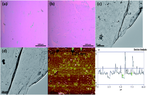 | ||
| Fig. 2 Graphene and BN doped graphene films grown on Cu using boric acid and nitrogen gas. (a) Optical images of pristine graphene transferred onto a SiO2/Si substrate. (b) Optical image of BN doped graphene transferred onto a SiO2/Si substrate. (c) Low-magnification TEM image of BN doped graphene on a plain Cu TEM grid showing a continuous graphene film. (d) High-magnification TEM image of BN doped graphene on a plain Cu grid showing small particles of Cu and Fe remaining after the etching process. (e) AFM image of BN doped graphene showing wrinkled graphene and (f) AFM section analysis of BN graphene showing an average film thickness of 1.25 nm. | ||
Raman spectra of pristine and BN doped graphene were taken from five different regions of both the doped and undoped graphene samples. Fig. 3 shows the comparison of the Raman spectra of one measurement from both the pristine and BN doped graphene. The Raman spectrum of pristine CVD graphene shows three peaks (1347, 1585 and at 2686 cm−1) representing the D, G and the 2D bands respectively (Table 1).25 Compared to the G and the 2D bands the D band has a very small intensity showing that the graphene is of high quality.25 The ratio between the intensity of the G to that of the 2D band (IG/I2D) is ca. 0.3 which suggests that the graphene has properties similar to that of a single layer graphene.24 The Raman spectrum of the BN doped graphene also showed three peaks (1341, 1589 and 2690 cm−1) again representing the D, G and the 2D bands respectively (Table 1).
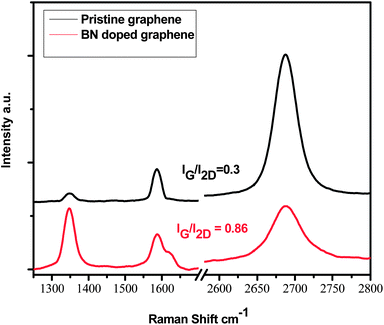 | ||
| Fig. 3 Raman spectra of pristine graphene and BN doped graphene synthesized using the CVD method on copper. | ||
The slight upshift of the G and 2D peaks of the doped graphene is associated with chemical doping into the graphene structure.26 The D band of the doped graphene showed a slight downshift. The doping is further corroborated by a shoulder on the G peak, also known as the D* peak, observed at 1623 cm−1. This split in the G peak of graphene has been reported previously by several authors and has been attributed to localized symmetry breaking in graphene,27–29 as found in BN doped graphene.22 The IG/I2D ratio of the BN doped graphene is 0.86, and the intensity of the 2D band is diminished in the BN doped graphene.
XPS data were recorded on the pristine and BN doped graphene. All spectra were recorded using an Al Kα microfocussed monochromatized source (1486.6 eV) with a resolution of 0.6 eV. The spot size was 400 μm and the operating pressure was 5 × 10⁻⁹ Pa. XPS data for pristine graphene revealed the presence of C and a small amount of O (not shown). The doped graphene by contrast showed peaks in the 400, 190 and 284 eV regions that correspond to N, B and C atoms respectively (Fig. 4). The atomic percentage of C, N and B in the sample was 98.0%, 1.38% and 0.62% respectively. The atomic percentage of the N and B dopants could be increased, but this was accompanied by an increase in the oxygen content and poor quality of the BN doped graphene that was produced.
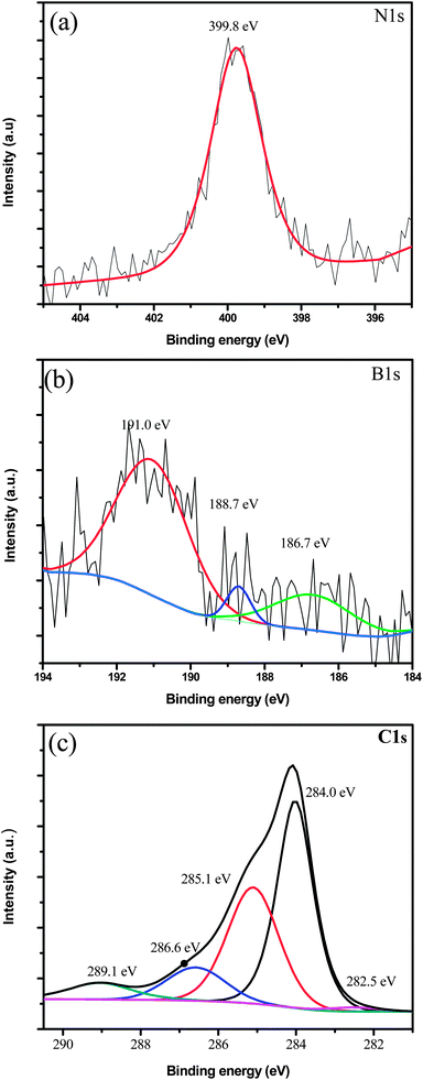 | ||
| Fig. 4 XPS spectra showing the (a) N1s, (b) B1s, and (c) C1s core levels obtained from BN doped graphene. | ||
Fig. 4a shows the N1s spectrum of BN doped graphene and reveals only a single peak at 399.8 eV. Since pure hexagonal boron nitride (h-BN)30 and BN doped graphene with discrete domains of BN alloyed with graphene22 give peaks at 398.1 eV, these types of structures can be ruled out in this new material. The peak at 399.8 eV is close to, but different from, the reported XPS peak energy of ∼401 eV for graphitic/quaternary N in graphene.31 The N1s peak position lies more toward the high binding energy region of a C–N bond. This suggests that there are more C–N bonds around a single N compared to B–N bonds. This is possible in a case where N is bonded to one B atom and two C atoms. These data suggest that the BN is not in the form of discrete domains (Fig. 6c) but is part of the extended graphene structure in the form of small BN domains shown in Fig. 6a and b.20
The B1s profile shown in Fig. 4b suggests that several B species are present and incorporated within the doped graphene product. The three peaks at ca. 191.0, 188.7 and 186.7 eV having different intensities indicate three B containing species with different concentrations. The large B1s peak at 191.0 eV can be associated with a boron atom linked to a nitrogen atom (BN structure).32,33 This is consistent with BN incorporation into graphene. The two boron species in lower concentrations, compared to the B in the BN, could correspond to BC3 at 188.7 eV (ref. 34 and 35) and to B4C at 186.7 eV (ref. 36) suggesting that C–B bonds are also present in the new material. However B–C bonds are very few meaning that, under the reaction conditions we have in this case (methane, boric acid and nitrogen gas), B–N formation is more favourable than B–C formation.
The C1s spectrum of the BN doped graphene (Fig. 4c) shows five peaks after deconvolution. The peak at 284.0 eV corresponds to sp2 hybridized carbon (graphitic carbon) from the undoped region of the graphene material.37 The peak at 285.1 eV can be associated with sp2 hybridized carbon bonded to nitrogen38 and to carbon with defects.39 The two peaks associated with sp2 hybridized carbon bonded to nitrogen and to carbon with defects overlap at 285.1 eV to form one peak. The peak at 285.1 eV likely arises from graphene domain edges and defects. The smaller peak at lower binding energy (282.5 eV) can be associated with B–C bond formation. The higher binding energy peaks at ca. 286.6 and 289.1 eV are attributed to the formation of C–O bonds.40
Fig. 5 shows the comparison of the C1s spectra of the pristine graphene with those of BN doped graphene. The C1s spectrum of pristine graphene has a more symmetrical shape and is very sharp when compared to the C1s spectra of the doped graphene. XPS analysis showed a downshift of 0.6 eV and broadening of the C1s peak after doping with BN. The downshift in the C1s peak of the doped material suggests that the material is a p-type semiconductor as was observed in doped p-type semiconducting carbon nanotubes.41 Experimental studies have shown that carbon films doped with both B and N exhibit p-type semiconducting behavior.42 Ambipolar semiconducting behavior was reported in a h-BNC material which contained discrete domains of graphene and h-BN.21 Analysis of the atomic composition of B and N atoms in our BN doped graphene showed that the B/N ratio was between 0.5 and 0.3, i.e., N was in excess in the graphene. This is possible because the N source in this reaction was nitrogen gas and this was in excess compared to the B from boric acid.
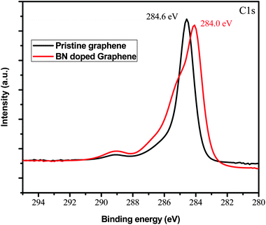
Fig. 6 shows three possible types of BN structures in the graphene matrix. Fig. 6a shows a BN species with a B/N ratio of 0.33 and Fig. 6b shows an h-BN structure with a B/N ratio of 0.5. The B/N ratio expected for Fig. 6c, which shows larger BN domains, is close to 1. The data hence suggest that small BN domains have been incorporated within the graphene matrix but not in large discrete BN domains.
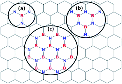 | ||
| Fig. 6 Atomic model of the possible BN species incorporated in BN doped graphene (a) BN with N bonded to 2 carbon atoms, (b) h-BN with the N bonded to one or two carbon atoms and (c) h-BN domains in the graphene matrix. | ||
We propose a mechanism for the formation of small BN domains within the extended graphene structure. Upon heating, H3BO3 in the copper container melts (171 °C) and volatilizes above 300 °C. The N2 carrier gas carries the H3BO3 to the copper foil (catalyst). Here the H3BO3 decomposes to form B2O3. Addition of CH4 at 995 °C results in the formation of reactive carbon species (eqn (1)).43 Reaction of C with B2O3 on the copper catalyst surface generates B–C species. However in the presence of N2, the B–C species are stabilized and form BN species in the graphene matrix (eqn (2)). The two reactions shown in eqn (1) and (2) take place on the copper surface. Reaction (2) is initiated by reaction (1). A similar mechanism has been used to explain the synthesis of BN doped single walled carbon nanotubes.44 Formation of BN in a graphene oxide material using graphene oxide material and B2O3 required a temperature of 1500 °C.33 In our case the reaction took place at 995 °C using the inert N source, N2 gas. The reaction can also be performed at low temperatures <1000 °C if the more reactive NH3 replaces the inert N2.43,45
| CH4(g) + H2(g) → C(s) + H2(g) | (1) |
| B2O3(s) + 3C(s) + N2(g) → BN(s) + 3CO(g) | (2) |
4 Conclusions
In summary, we have synthesized large area graphene incorporating small BN species by a facile and safe process avoiding the use of boranes and ammonia. Raman analysis reveals formation of monolayer (or few layer) BN doped graphene. XPS revealed that several B bonding species were incorporated into graphene with the main product being the small BN domains. The N of the BN is bonded to carbon forming B–N–C systems, showing that we managed to grow continuous BN containing graphene in which BN species were incorporated in the graphene structure. This remarkable finding has led us to synthesize large area graphene incorporating small BN domains. The method is a simple one. Raman data revealed an additional D* band in the BN doped graphene that confirmed possible band gap opening by graphene symmetry breaking. The results presented here are highly relevant to the application of graphene in nano-optoelectronic devices.Acknowledgements
This work was supported financially by the NRF, the DST/NRF Center of Excellence in Strong Materials and the University of the Witwatersrand. MC would like to acknowledge funding from the NSF IGERT (0903661) program. GB would like to acknowledge Dr Johanna Bernstein and Professor Eric Garfunkel for facilitating the IGERT matching support from Rutgers University for his visit to Rutgers University. DV acknowledges funding from Rutgers University. We are in debt to Dr Manoko Maubane and Thuto Makgato for their kind help with TEM and AFM respectively.Notes and references
- K. S. Novoselov, A. K. Geim, S. V. Morozov, D. Jiang, Y. Zhang, S. V. Dubonos, I. V. Grigorieva and A. A. Firsov, Science, 2004, 306, 666–669 CrossRef CAS.
- A. H. Castro Neto, F. Guinea, N. M. R. Peres, K. S. Novoselov and A. K. Geim, Rev. Mod. Phys., 2009, 81, 109–162 CrossRef CAS.
- C. Stamfer, S. Fringes, J. Guttinger, F. Molitor, C. Volk, B. Terres, J. Dauber, S. Engels, S. Schnez, A. Jacobsen, S. Droscher, T. Ihn and K. Ensslin, Front. Phys., 2011, 6, 271–293 CrossRef.
- S. Ghosh, I. Calizo, D. Teweldebrhan, E. P. Pokatilov, D. L. Nika, A. A. Balandin, W. Bao, F. Miao and C. N. Lau, Appl. Phys. Lett., 2008, 92, 151911 CrossRef.
- Y. Zhu, S. Murali, W. Cai, X. Li, J. W. Suk, J. R. Potts and R. S. Ruoff, Adv. Mater., 2010, 22, 3906–3924 CrossRef CAS.
- S. S. Li, K. H. Tu, C. C. Lin, C. W. Chen and M. Chhowalla, ACS Nano, 2010, 4, 3169–3174 CrossRef CAS.
- X. Wang, L. Zhi and K. Müellen, Nano Lett., 2008, 8, 323–327 CrossRef CAS.
- H. Liu, Y. Liu and D. J. Zhu, J. Mater. Chem., 2011, 21, 3335–3345 RSC.
- J. M. Schnorr and T. M. Swager, Chem. Mater., 2011, 23, 646–657 CrossRef CAS.
- W. Chen, S. Chen, D. C. Qi, X. Y. Gao and A. T. S. Wee, J. Am. Chem. Soc., 2007, 129, 10418–10422 CrossRef CAS.
- H. Miao, S. Tongay, M. K. Petterson, K. Berke, A. G. Rinzler, B. R. Appleton and A. F. Hebard, Nano Lett., 2012, 12, 2745–2750 CrossRef.
- K. F. Mak, C. H. Lui, J. Shan and T. F. Heinz, Phys. Rev. Lett., 2009, 102, 256405 CrossRef.
- L. S. Panchakarla, K. S. Subrahmanyam, S. K. Saha, A. Govindaraj, H. R. Krishnamurthy, U. V. Waghmare and C. N. R. Rao, Adv. Mater., 2009, 21, 4726–4730 CAS.
- C. Zhang, L. Fu, N. Liu, M. Liu, Y. Wang and Z. Liu, Adv. Mater., 2011, 23, 1020–1024 CrossRef CAS.
- Y. Wang, Y. Shao, D. W. Matson, J. Li and Y. Lin, ACS Nano, 2010, 4, 1790–1798 CrossRef CAS.
- Z. H. Sheng, H. L. Gao, W. J. Bao, F. B. Wang and W. H. Xia, J. Mater. Chem., 2012, 22, 390–395 RSC.
- S. Suzuki and H. Hibino, Mater. Sci. Eng., B, 2012, 177, 233–238 CrossRef CAS.
- P. P. Shinde and V. Kumar, Phys. Rev. B: Condens. Matter Mater. Phys., 2011, 84, 125401 CrossRef.
- B. Xu, Y. H. Lu, Y. P. Feng and J. Y. Lin, J. Appl. Phys., 2010, 108, 073711–073717 CrossRef.
- X. Fan, Z. Shen, A. Q. Liu and J. Kuo, Nanoscale, 2012, 4, 2157–2165 RSC.
- Y. Lin and J. W. Connell, Nanoscale, 2012, 4, 6908–6939 RSC.
- L. Ci, L. Song, C. Jin, D. Jariwala, D. Wu, Y. Li, A. Srivastava, Z. F. Wang, K. Storr, L. Balicas, F. Liu and P. M. Ajayan, Nat. Mater., 2010, 9, 430–435 CrossRef CAS.
- X. Li, W. Cai, J. An, S. Kim, J. Nah, D. Yang, R. Piner, A. Velamakanni, I. Jung, E. Tutuc, S. K. Banerjee, L. Colombo and R. Ruoff, Science, 2009, 324, 1312–1314 CrossRef CAS.
- C. Mattevi, H. Kim and M. Chhowalla, J. Mater. Chem., 2011, 21, 3324–3334 RSC.
- A. C. Ferrari, J. C. Meyer, V. Scardaci, C. Casiraghi, M. Lazzeri, F. Mauri, S. Piscanec, D. Jiang, K. S. Novoselov, S. Roth and A. K. Geim, Phys. Rev. Lett., 2006, 97, 187401 CrossRef CAS.
- C. Casiraghi, S. Pisana, K. S. Novoselov, A. K. Geim and A. C. Ferrari, Appl. Phys. Lett., 2007, 91, 233108 CrossRef.
- X. Dong, Y. Shi, Y. Zhao, D. Chen, J. Ye, Y. Yao, F. Gao, Z. Ni, T. Yu, Z. Shen, Y. Huang, P. Chen and L. Li, Phys. Rev. Lett., 2009, 102, 135501 CrossRef.
- R. Yang, Q. S. Huang, X. Chen, G. Y. Zhang and H. J. Gao, J. Appl. Phys., 2010, 107, 034305 CrossRef.
- J. Lee, K. S. Novoselov and H. S. Shin, ACS Nano, 2011, 5, 608–612 CrossRef CAS.
- C. Guimon, D. Gonbeau, G. Pfister-Guillouzo, O. Dugne, A. Guette, R. Naslain and M. Lahaye, Surf. Interface Anal., 1990, 16, 440–445 CrossRef CAS.
- J. O. Hwang, J. S. Park, D. S. Choi, J. Y. Kim, S. H. Lee, K. E. Lee, Y. H. Kim, M. H. Song, S. Yoo and S. O. Kim, ACS Nano, 2012, 6, 159–167 CrossRef CAS.
- K. S. Park, D. Y. Lee, K. J. Kim and D. W. Moon, Appl. Phys. Lett., 1997, 70, 315–317 CrossRef CAS.
- T. W. Lin, C. Y. Su, X. Q. Zhang, W. Zhang, Y. H. Lee, C. W. Chu, H. Y. Lin, M. T. Chang, F. R. Chen and L. J. Li, Small, 2011, 8, 1384–1391 CrossRef.
- W. Cermignani, T. E. Paulson, C. Onneby and C. G. Pantano, Carbon, 1995, 33, 367–374 CrossRef CAS.
- L. G. Jacobsohn, R. K. Schulze, M. E. H. Maia da Costa and M. Nastasi, Surf. Sci., 2004, 572, 418–424 CrossRef CAS.
- E. A. Il'inchik, V. V. Volkov and L. N. Mazalov, J. Struct. Chem., 2005, 46, 523–534 CrossRef CAS.
- E. Moreau, F. J. Ferrer, D. Vignaud, S. Godey and S. Wallart, Phys. Status Solidi A, 2010, 207, 300–303 CrossRef CAS.
- Y. Shao, S. Zhang, M. H. Engelhard, G. Li, G. Shao, Y. Wang, J. Liu, I. A. Aksayc and Y. Lin, J. Mater. Chem., 2010, 20, 7491–7496 RSC.
- Z. Q. Luo, J. Z. Shang, S. H. Lim, D. H. Li, Q. H. Xiong, Z. X. Shen, J. Y. Lin and T. Yu, Appl. Phys. Lett., 2010, 97, 233111 CrossRef.
- C. Morant, P. J. Prieto, J. Bareño, M. Sanz and E. Elizalde, Thin Solid Films, 2006, 515, 207–211 CrossRef CAS.
- H. Z. Geng, K. K. Kim, C. Song, N. T. Xuyen, S. M. Kim, K. A. Park, D. S. Lee, K. H. An, Y. S. Lee, Y. Chang, Y. J. Lee, J. Y. Choi, A. Benayad and Y. H. Lee, J. Mater. Chem., 2008, 18, 1261–1266 RSC.
- M. O. Watanabe, S. Itoh, K. Mizushima and T. Sasaki, J. Appl. Phys., 1995, 78, 2880 CrossRef CAS.
- P. Ammendola, R. Chirone, L. Lisi, G. Ruoppolo and G. Russo, J. Mol. Catal. A: Chem., 2007, 266, 31–39 CrossRef CAS.
- W. L. Wanga, J. Q. Bia, W. X. Suna, H. L. Zhua, J. J. Xua, M. T. Zhaoa and Y. J. Bai, Mater. Chem. Phys., 2010, 122, 129–132 CrossRef.
- J. Thomas, N. E. Weston and T. E. O'Connor, J. Am. Chem. Soc., 1962, 84, 4619–4622 CrossRef CAS.
Footnote |
| † Current address: Renewable Energy and Energy Efficiency Institute, Polytechnic of Namibia, 13 Storch Street, Private bag 13388, Windhoek, Namibia. |
| This journal is © The Royal Society of Chemistry 2013 |