DOI:
10.1039/C3NR01419C
(Communication)
Nanoscale, 2013,
5, 6243-6248
Reflective plasmonic color filters based on lithographically patterned silver nanorod arrays
Received
22nd March 2013
, Accepted 19th April 2013
First published on 23rd April 2013
Abstract
We demonstrate reflection-mode plasmonic color filters based on lithographically patterned silver nanorods with ultrasmall inter-rod gaps. Fine and effective tuning of the plasmon resonance is shown by varying array periodicities. We determine the dependence of reflected intensity on diameter/periodicity ratio and then develop reflective plasmonic color filters using dense nanorod arrays. Experimental results agree well with theoretical calculations. Our approach is potentially useful for plasmon-assisted sensing, imaging and displays.
Introduction
Plasmonics provides the unique capability of manipulating light at sub-wavelength scales by using versatile nanostructures, such as cubes,1–3 clusters,4–6 shells,7,8 disks,9–11 holes,12,13 rings,14,15 rods,16–20 and particles with arbitrary shapes.21–23 Many different kinds of plasmonic device have been demonstrated so far, including modulators,24 interferometers,25 switches,26,27 polarizers,28,29 and absorbers.30–33 Color filters are an essential component in imaging sensors, color displays, digital cameras, and other related applications. Recently, interest in plasmon-assisted color filters has greatly increased due to their ultracompact design, ultrahigh resolution, and convenient integration. So far, various plasmonic color filters, such as nanoslits with periodical grooves,34 metal–insulator–metal stacks,35,36 and annular aperture arrays,37–39 have been demonstrated. However, most efforts have been concentrated on transmission-mode color filters instead of reflection-mode ones. Very recently, researchers have shown that it is feasible to control colors using functional “intaglio/bas-relief”40 or nanodisks with backreflector41 under reflection mode.
Metallic nanorod arrays with preferred alignment and periodicities are of particular importance for surface plasmon resonances and couplings, hence affecting photon flow accordingly.42 However, it is very challenging to fabricate a dense nanorod array with ultrasmall gaps and large aspect ratios using normal lift-off methods. In this communication, we fabricate dense silver nanorod arrays with ultrasmall gaps through electron-beam lithography (EBL) followed by ion milling. The effects of periodicity (p) and diameter/periodicity (d/p) ratio of the silver nanorod arrays on the plasmon resonance are investigated. By controlling their geometries, we show that such nanorod arrays are capable of tuning the plasmon resonance and further reflectively filtering out individual colors from a broadband light source. Hence, they can serve as reflective plasmonic color filters, which may find extensive application ranging from color filtering to spectral imaging.
Methods
Fabrication of dense silver nanorod arrays
An optically thick (180 nm) silver film was deposited on a quartz substrate with a 6 nm titanium adhesion layer by electron-beam evaporation. Prior to the film deposition, the substrate was cleaned with acetone followed by deionized water and blown dry with a nitrogen gun. To minimize the roughness introduced by deposition, a low evaporation rate was employed (less than 0.05 nm s−1). Both titanium and silver films were deposited sequentially on the quartz substrate using an Edwards Auto 306 electron-beam evaporator at a base pressure of about 2 × 10⁻⁷ mbar. Negative resist NEB 22 of around 320 nm thickness was selected as the ion milling mask after EBL patterning and development. The area of each array was ∼8 × 8 μm2. During ion milling (INTLVAC NANOQUEST), argon ions impinged upon the sample surface at an angle of 10°. The beam voltage was 300 V with 45 V accelerating voltage and 110 mA beam current. The total milling time was around 4 minutes with the power stabilized around 156 W. Resist residue was removed by Microposit Remover 1165 after ion milling.
Optical characterization
The optical response of the fabricated nanorods was measured using a UV-Vis-NIR microspectrometer (CRAIC QDI 2010™) at normal incidence with a 75 W broadband xenon source. We used a reflecting objective (magnification: 36×; numerical aperture: 0.5) to shine the white light onto the samples and collect the reflected light to both spectrometer and colored CCD simultaneously. The detecting area was limited to 7.1 × 7.1 μm2 using a variable aperture. Reflection and transmission measurements were normalized with respect to an aluminium mirror and a bare quartz substrate, respectively.
FDTD simulations
Finite-difference time-domain (FDTD) simulations were performed using Lumerical packages.43 The dispersion model of silver is based on data from Johnson and Christy44 in the material library of the software. The simulation model was built based on the schematic shown in Fig. 1. One set of four silver nanorods was modelled with thickness ranging from 140 nm to 180 nm, providing a good agreement with experimental results. Note that the 6 nm titanium layer was also taken into account in our simulations. The dimension of the simulation area was set so as to allow two periods of the nanorod structure in the x–y plane and enough space for the light source and power monitors. Auto-nonuniform meshing with the finest meshes (0.25 nm minimum mesh step) was used to achieve the most accurate results. The auto-cutoff was set at 1 × 10⁻⁶ to ensure the convergence of the obtained results. Simulation time was set as 1000 μs with a step of 0.015 μs. The results usually converged before the simulation time ran out. The light source covered wavelengths ranging from 300 nm to 1300 nm with an increasing step of 2 nm. A power monitor was located 300 nm above the silver rods and 100 nm above the light source to collect reflected and scattered modes reaching the detecting region.
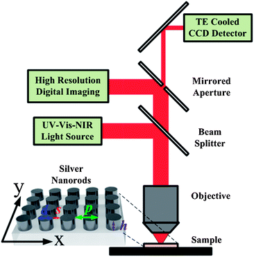 |
| | Fig. 1 Schematic diagram of the color filter working in reflection mode. | |
Results and discussion
Fig. 1 illustrates the schematic view of the optical setup to characterize a reflective plasmonic color filter. Silver nanorod arrays with different periodicities were fabricated on a quartz substrate using standard EBL (Elionix ELS-7000) processes followed by ion milling. Fig. 2a is the scanning electron microscope (SEM) image of a representative sample with the structural parameters: periodicity p = 550 nm in both x- and y-directions (see Fig. 1), rod diameter d = 275 nm (d/p = 0.5), and height h = 180 nm. Fig. 2b plots the measured reflection spectra of nanorod arrays with large inter-rod gaps (s ≥ 200 nm) and varying periodicities from 400 nm (d = 200 nm) to 700 nm (d = 350 nm) in 50 nm increments (i.e., the d/p ratio was kept constant at 0.5). As can be seen from Fig. 2b, the reflection spectra can be tuned across the near infrared range with various array periodicities. A shift in resonance peaks from 750 nm to 1270 nm is observed when the periodicity is increased from 400 nm to 700 nm. The reflected intensity varies within 10% and the full-width at half-maximum (FWHM) decreases noticeably at smaller periodicities. Fig. 2c plots the simulated reflection spectra based on the experimentally achieved structural data using the FDTD method. There are obvious differences between measurements and simulations (see Fig. 2b and c): experimental results show that the main resonance peaks become broader and show lower reflectance with increased periodicity; while simulations show that the FWHM remains almost constant and that reflectance becomes greater. These differences could be attributed to larger scattering in experiments compared to simulations, which causes broader FWHM and lower reflectance with increased periodicity. The larger scattering effect may arise from: (1) shape difference between the simulation model (perfect cylindrical rod) and the real sample (dome-like profile and non-circle shape); (2) surface oxidation of silver nanorods;45,46 (3) nonuniform silver materials properties caused by different grain sizes and distribution during metal deposition. Nevertheless, the simulation results show qualitative agreement with experiments and thus confirm our design concept.
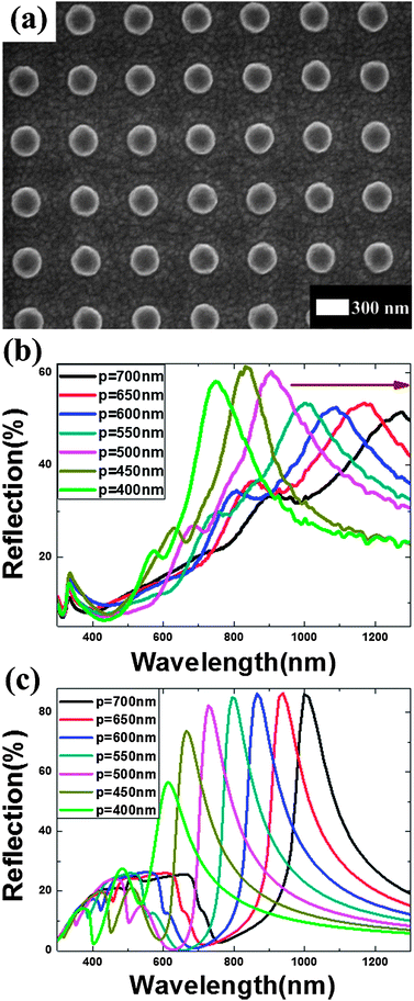 |
| | Fig. 2 (a) SEM image showing the top view of a silver nanorod array with period p = 550 nm. (b) Measured and (c) calculated reflection spectra for nanorod arrays with periodicities from 400 nm to 700 nm. The arrow indicates increasing periodicities. | |
Complex mechanisms are involved when periodical plasmonic nanorod arrays are illuminated with light, including localized surface plasmon resonance (LSPR), Wood's anomalies and Bloch wave surface plasmon polaritons.47 The collective plasmonic resonances at different wavelengths are the combined results of all three effects and their mutual coupling. LSPR can be estimated using the coupling dipole theory, which has been developed and discussed comprehensively elsewhere.48,49 Each single rod can be modelled by a dipole of polarizability α, which can be written as:50
| |  | (1) |
where
εm and
εd are the relative permittivities of metal and surrounding environment, respectively.
χ is the shape factor relating to the physical shape of the
nanorod and
V is the volume of the
nanorod. When the
nanorod array is excited by an electromagnetic field with frequency
ω, the rod dipole will radiate a scattering field in proportion to its dipole moment. The total LSPR field with an effective polarizability
α* is a combined effect of the incident field and radiation from each individual
nanorods, which can be expressed as:
50| |  | (2) |
with the array factor
S denoting the collective effect of all
nanorods and depending only on the geometrical factors of the
nanorods. The
S factor for a square array of
nanorods under normal incidence can be written as:
50| |  | (3) |
A peak in the reflection spectrum can be achieved when the condition S = 1/α is satisfied, which is the theoretical basis upon which to build our color filter since designated wavelengths can be separated by varying the sizes and periods of nanorod arrays.
To further investigate the impact of inter-rod gaps on the optical response of nanorods, we calculate the reflections in the visible range for nanorod arrays with constant periodicity p = 400 nm and varying inter-rod gaps and diameter sizes, as shown in Fig. 3. The peak intensity increases with larger d/p values, which is caused by the reduced distance between adjacent nanorods. As the gap size decreases to several tens of nanometers, the converted surface plasmon waves from the incident light will not enter the structure because the ultrasmall gaps between nanorods allow nothing but zero plasmon modes,51,52 which cannot penetrate the nanorod layers of 180 nm. Most of the waves will only exist at the interface of air/rods and will be decoupled back into propagating electromagnetic waves as the reflection towards the incident direction. Apart from the intrinsic absorption and the damping loss of the surface plasmon waves, most of the input light energy reflects back as resonance peaks where the surface plasmon waves can be excited and the intensity will increase as the size of the gap decreases, which will be confirmed by the following experiments.
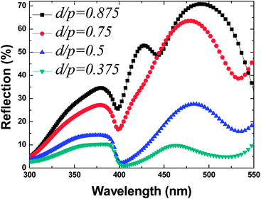 |
| | Fig. 3 Calculated reflection of nanorod arrays with constant periodicity p = 400 nm and varying inter-rod gaps and diameters corresponding to different d/p values ranging from 0.375 to 0.875. | |
To experimentally demonstrate the reflection-mode color filter, we fabricated plasmonic color filters according to the design with different d/p values and dramatically decreased inter-rod gaps. SEM images of nanorods with different inter-rod gaps are shown in Fig. 4. The silver rods have been milled through and very small (20–40 nm) inter-rod gaps can be clearly observed. Using nanorods with different periodicities from 540 nm (Fig. 4a) to 320 nm (Fig. 4e) with a step size of 55 nm, we filtered individual colors out as shown in Fig. 5a. From the top view of the rods (Fig. 4f), ultrasmall inter-rod gap sizes (∼25 nm) can be clearly observed. The structural parameters of the arrays are summarized in Table 1. As expected, strong optical excitations in the visible band of the spectrum are observed. By changing the periodicity of the nanorod arrays, tuning of the resonance peak wavelengths between 480 nm (blue) to 630 nm (red) is achieved, as shown in Fig. 5b. One can see that when the periodicity is 540 nm (s = 40 nm), a broad resonance is located at ∼630 nm. When the periodicity is reduced to 485 nm (s = 35 nm), the resonance peak shifts to about 580 nm, exhibiting a yellow color. Furthermore, when the periodicity is smaller than 430 nm, narrower resonance peaks are distinct and more reflected energies are observed due to stronger coupling in the small cavities, displaying as green, cyan and blue, respectively. Note that more intensity is reflected as the periodicity is decreased. The relatively large FWHM of the curve for the blue color compared to other spectra is due to fabrication imperfections. Some of the rods are touching each other (see Fig. 4e). Once the conductive contact between rods is established, the original surface charge distribution is broken and a different regime is formed. The conductive coupling between nanorods leads to redistribution of surface charges, resulting in the mergence of separate individual modes. Fig. 5c presents the measured transmission spectra which show relatively low intensities (less than 20% in the visible range), leading to a high efficiency reflective color filter.
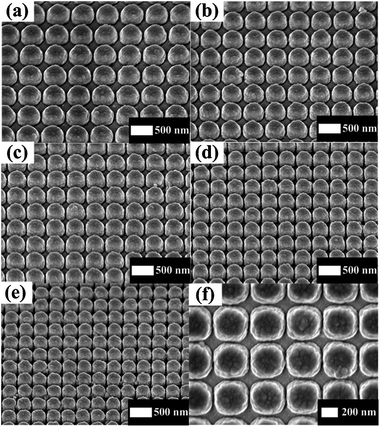 |
| | Fig. 4 SEM images showing oblique views of dense nanorod arrays with different periodicities from (a) 540 nm to (e) 320 nm with a step size of 55 nm. (f) Magnified top view of (d) with p = 375 nm and d = 350 nm. | |
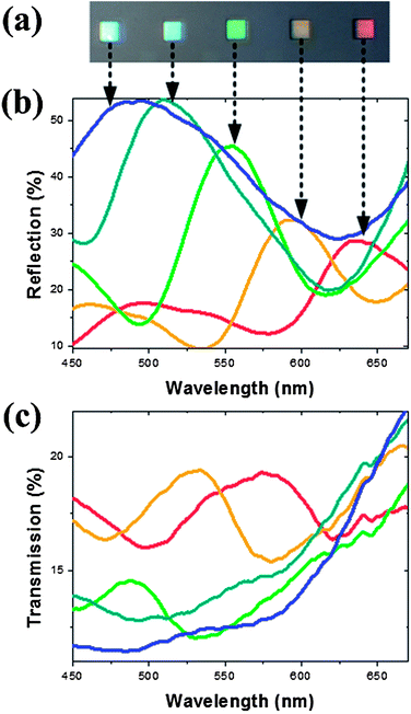 |
| | Fig. 5 (a) Optical image showing the reflective colors from different silver nanorod arrays. Measured reflection (b) and transmission (c) spectra of the corresponding arrays as a function of wavelengths. | |
Table 1 Optimized parameters of the nanorod arrays and the corresponding reflected colors
| Presented color |
Periodicity (nm) |
Rod diameter (nm) |
Gap (nm) |
d/p |
| Red |
540 |
500 |
40 |
0.926 |
| Yellow |
485 |
450 |
35 |
0.928 |
| Green |
430 |
400 |
30 |
0.930 |
| Cyan |
375 |
350 |
25 |
0.933 |
| Blue |
320 |
300 |
20 |
0.938 |
Conclusions
In summary, we have demonstrated tuning of the plasmon resonance using dense plasmonic nanorod arrays. The optical response depends strongly on the periodicity of the arrays and the diameter/periodicity ratio. Effective tuning of surface plasmon resonance peaks is achieved across the near infrared range using plasmonic nanorod arrays with inter-rod gaps larger than 200 nm. The reflection peaks coincide with the plasmon resonance and nanorod arrays with different periodicities can act as color filters suitable for reflection measurement. Individual colors are demonstrated by using dense plasmonic nanorods with ultrasmall inter-rod gaps smaller than 40 nm and different array periodicities. A variety of applications such as sensing, imaging and displays can be readily realized by varying either the geometry or the surrounding media of the nanorods.
Acknowledgements
The authors thank Joey Rufo for helpful discussions. This work was partially supported by A*STAR under grant no. 0921540099, NEU internal funding XNB201302 and Natural Science Foundation of Hebei Province under grant no. A2013501049. N. Xiang thanks the funding support from Singapore Ministry of Education under grant no. MOE2009-T2-1-086.
Notes and references
- H. J. Chen, Z. H. Sun, W. H. Ni, K. C. Woo, H.-Q. Lin, L. D. Sun, C. H. Yan and J. F. Wang, Small, 2009, 5, 2111–2119 CrossRef CAS
 .
.
- X. S. Kou, Z. H. Sun, Z. Yang, H. J. Chen and J. F. Wang, Langmuir, 2009, 25, 1692–1698 CrossRef CAS .
- X. Wu, T. Ming, X. Wang, P. N. Wang, J. F. Wang and J. Y. Chen, ACS Nano, 2010, 4, 113–120 CrossRef CAS .
- J. B. Lassiter, H. Sobhani, J. A. Fan, J. Kundu, F. Capasso, P. Nordlander and N. J. Halas, Nano Lett., 2010, 10, 3184–3189 CrossRef CAS .
- J. A. Fan, C. Wu, K. Bao, J. Bao, R. Bardhan, N. J. Halas, V. N. Manoharan, P. Nordlander, G. Shvets and F. Capasso, Science, 2010, 328, 1135–1138 CrossRef CAS .
- J. A. Fan, K. Bao, C. Wu, J. Bao, R. Bardhan, N. J. Halas, V. N. Manoharan, G. Shvets, P. Nordlander and F. Capasso, Nano Lett., 2010, 10, 4680–4685 CrossRef CAS .
- J. B. Lassiter, J. Aizpurua, L. I. Hernandez, D. W. Brandl, I. Romero, S. Lal, J. H. Hafner, P. Nordlander and N. J. Halas, Nano Lett., 2008, 8, 1212–1218 CrossRef CAS .
- R. Bardhan, N. K. Grady, T. Ali and N. J. Halas, ACS Nano, 2010, 4, 6169–6179 CrossRef CAS .
- I. Zorić, E. M. Larsson, B. Kasemo and C. Langhammer, Adv. Mater., 2010, 22, 4628–4633 CrossRef .
- C. Langhammer, M. Schwind, B. Kasemo and I. Zorić, Nano Lett., 2008, 8, 1461–1471 CrossRef CAS .
- Y. J. Liu, Y. B. Zheng, J. Liou, I.-K. Chiang, I. C. Khoo and T. J. Huang, J. Phys. Chem. C, 2011, 115, 7717–7722 CAS .
- T. W. Ebbesen, H. J. Lezec, H. F. Ghaemi, T. Thio and P. A. Wolff, Nature, 1998, 391, 667–669 CrossRef CAS .
- Y. J. Liu, E. S. P. Leong, B. Wang and J. H. Teng, Plasmonics, 2011, 6, 659–664 CrossRef CAS .
- P. Nordlander, ACS Nano, 2009, 3, 488–492 CrossRef CAS .
- A. R. Halpern and R. M. Corn, ACS Nano, 2013, 7, 1755–1762 CrossRef CAS .
- H. J. Chen, L. Shao, Q. Li and J. F. Wang, Chem. Soc. Rev., 2013, 42, 2679–2724 RSC .
- Y. D. Zheng, M. D. Xiao, S. X. Jiang, F. Ding and J. F. Wang, Nanoscale, 2013, 5, 788–795 RSC .
- G. A. Wurtz, R. Pollard, W. Hendren, G. P. Wiederrecht, D. J. Gosztola, V. A. Podolskiy and A. V. Zayats, Nat. Nanotechnol., 2011, 6, 107–111 CrossRef CAS .
- G. A. Wurtz, W. Dickson, D. O'Connor, R. Atkinson, W. Hendren, P. Evans, R. Pollard and A. V. Zayats, Opt. Express, 2008, 16, 7460–7470 CrossRef CAS .
- D. P. Lyvers, J. M. Moon, A. V. Kildishev, V. M. Shalaev and A. Wei, ACS Nano, 2008, 2, 2569–2576 CrossRef CAS .
- A. M. Kern and O. J. F. Martin, Nano Lett., 2011, 11, 482–487 CrossRef CAS .
- J. P. Kottmann, O. J. F. Martin, D. R. Smith and S. Schultz, Opt. Express, 2000, 6, 213–219 CrossRef CAS .
- A. Lovera and O. J. F. Martin, Appl. Phys. Lett., 2011, 99, 151104 CrossRef .
- J. A. Dionne, K. Diest, L. A. Sweatlock and H. A. Atwater, Nano Lett., 2009, 9, 897–902 CrossRef CAS .
- M. J. Dicken, L. A. Sweatlock, D. Pacifici, H. J. Lezec, K. Bhattacharya and H. A. Atwater, Nano Lett., 2008, 8, 4048–4052 CrossRef CAS .
- Y. J. Liu, Q. Hao, J. S. T. Smalley, J. Liou, I. C. Khoo and T. J. Huang, Appl. Phys. Lett., 2010, 97, 091101 CrossRef .
- R. A. Pala, K. T. Shimizu, N. A. Melosh and M. L. Brongersma, Nano Lett., 2008, 8, 1506–1510 CrossRef CAS .
- X. Zhang, H. Liu, J. Tian, Y. Song and L. Wang, Nano Lett., 2008, 8, 2653–2658 CrossRef CAS .
- Y. Zhao, M. A. Belkin and A. Alù, Nat. Commun., 2012, 3, 870 CrossRef CAS .
- N. Liu, M. Mesch, T. Weiss, M. Hentschel and H. Giessen, Nano Lett., 2010, 10, 2342–2348 CrossRef CAS .
- Y. Wang, T. Sun, T. Paudel, Y. Zhang, Z. Ren and K. Kempa, Nano Lett., 2012, 12, 440–445 CrossRef CAS .
- K. Aydin, V. E. Ferry, R. M. Briggs and H. A. Atwater, Nat. Commun., 2011, 2, 517 CrossRef .
- Y. Zhao, Q. Hao, Y. Ma, M. Lu, B. Zhang, M. Lapsley, I. C. Khoo and T. J. Huang, Appl. Phys. Lett., 2012, 100, 053119 CrossRef .
- E. Laux, C. Genet, T. Skauli and T. W. Ebbesen, Nat. Photonics, 2008, 2, 161–164 CrossRef CAS .
- W. Cai, U. K. Chettiar, H. K. Yuan, V. C. de Silva, A. V. Kildishev, V. P. Drachev and V. M. Shalaev, Opt. Express, 2007, 15, 3333–3341 CrossRef .
- T. Xu, Y. K. Wu, X. G. Luo and L. J. Guo, Nat. Commun., 2010, 1, 59 Search PubMed .
- G. Y. Si, Y. H. Zhao, H. Liu, S. L. Teo, M. S. Zhang, T. J. Huang, A. J. Danner and J. H. Teng, Appl. Phys. Lett., 2011, 99, 033105 CrossRef .
- Y. J. Liu, G. Y. Si, E. S. P. Leong, B. Wang, A. J. Danner, X. C. Yuan and J. H. Teng, Appl. Phys. A: Mater. Sci. Process., 2012, 107, 49–54 CrossRef CAS .
- Y. J. Liu, G. Y. Si, E. S. P. Leong, N. Xiang, A. J. Danner and J. H. Teng, Adv. Mater., 2012, 24, OP131–OP135 CrossRef CAS .
- J. Zhang, J. Ou, N. Papasimakis, Y. Chen, K. F. MacDonald and N. I. Zheludev, Opt. Express, 2011, 19, 23279–23285 CrossRef CAS .
- K. Kumar, H. Duan, R. S. Hegde, S. C. W. Koh, J. N. Wei and J. K. W. Yang, Nat. Nanotechnol., 2012, 7, 557–561 CrossRef CAS .
- G. Y. Si, Y. H. Zhao, J. T. Lv, F. W. Wang, H. L. Liu, J. H. Teng and Y. J. Liu, Nanoscale, 5, 4309–4313 RSC .
- Lumerical FDTD solution: http://www.lumerical.com/.
- P. B. Johnson and R. W. Christy, Phys. Rev. B: Solid State, 1972, 6, 4370–4379 CrossRef CAS .
- E. S. P. Leong, Y. J. Liu, B. Wang and J. H. Teng, ACS Appl. Mater. Interfaces, 2011, 3, 1148–1153 CAS .
-
E. S. P. Leong, Y. J. Liu, C. C. Chum and J. H. Teng, Plasmonics 201381221–1226 Search PubMed.
- K. Lee and P. Wei, Small, 2010, 6, 1900–1907 CrossRef CAS .
- S. Zou and G. C. Schatz, Nanotechnology, 2006, 17, 2813–2820 CrossRef CAS .
- V. A. Markel and A. K. Sarychev, Phys. Rev. B: Condens. Matter Mater. Phys., 2007, 75, 085426 CrossRef .
- B. Auguié and W. L. Barnes, Phys. Rev. Lett., 2008, 101, 143902 CrossRef .
- M. J. Levene, J. Korlach, S. W. Turner, M. Foquet, H. G. Craighead and W. W. Webb, Science, 2003, 299, 682–686 CrossRef CAS .
- M. Foquet, K. T. Samiee, X. Kong, B. P. Chauduri, P. M. Lundquist, S. W. Turner, J. Freudenthal and D. B. Roitman, J. Appl. Phys., 2008, 103, 034301 CrossRef .
Footnote |
| † These authors contributed equally to this work. |
|
| This journal is © The Royal Society of Chemistry 2013 |
Click here to see how this site uses Cookies. View our privacy policy here.  Open Access Article
 This Open Access Article is licensed under a Creative Commons Attribution-Non Commercial 3.0 Unported Licence