 Open Access Article
 This Open Access Article is licensed under a
 Creative Commons Attribution 3.0 Unported Licence
Electrically conductive magnetic nanowires using an electrochemical DNA-templating route†
Scott M. D.
Watson‡
a,
Hasan Daw A.
Mohamed‡
ab,
Benjamin R.
Horrocks
a and
Andrew
Houlton
*a
aChemical Nanoscience Laboratory, School of Chemistry, Newcastle University, Newcastle-Upon-Tyne, NE1 7RU, UK. E-mail: andrew.houlton@ncl.ac.uk
bChemistry Department, Faculty of Arts and Science, Azzaytuna University, P.O. Box 39011/39010, Tarhuna, Libya
First published on 24th April 2013
Abstract
The fabrication of electrically conducting magnetic nanowires has been achieved using electrochemical DNA-templating of iron. In this approach, binding of the Fe2+ cations to the DNA “template” molecules has been utilised to promote growth along the molecular axis. Formation of Fe within the product material was verified by XRD and XPS studies, which confirmed an iron/oxide “core–shell” structure. The effectiveness of the DNA duplex to direct the metal growth in one dimension was highlighted by AFM which reveals the product material to comprise high aspect ratio nanostructured architectures. These “nanowires” were observed to have morphologies consisting of densely packed linear arrangements of metal particles along the template, with wire diameters up to 26 nm. The structures were confirmed to be electrically conductive, as expected for such Fe-based materials, and to display superparamagnetic behaviour, consistent with the small size and particulate nature of the nanowires.
Introduction
The ability to form structurally well-defined materials on the nanometre scale is of great interest within the scientific and technological communities.1,2 The distinct properties which materials exhibit when one or more of their physical dimensions is so reduced presents enormous potential for their exploitation in a variety of applications. The most ambitious of these is their anticipated role as building blocks for the construction of nanoscale devices through so-called “bottom-up” approaches. One-dimensional (1-D) nanostructured materials (e.g. nanowires, nanorods, and nanotubes)2–4 are one such class which has received much attention to date.Electrochemical growth is amongst the most common approaches to the fabrication of 1-D nanostructures. Such methods are useful as they can be carried out under ambient conditions, afford considerable control over material formation, are of low cost in implementation, and have potential for scale-up. They have also been shown to offer good versatility with a wide range of material types being produced, including metals (e.g. Fe, Ni, Co, Pt), inorganic semiconductors (e.g. CdSe, ZnO), and organic conducting polymers (e.g. polyaniline, polypyrrole).5–14 Generally, the application of electrochemical methods for nanowire fabrication has involved the use of a porous membrane such as anodically etched aluminium oxide (AAO),5–7 polycarbonate track membranes,8 or porous silica,10,11 supported upon an electrode at which electrodeposition takes place. In this way the porous membrane confines the material growth from the electrode surface to individual channels resulting in uniaxial growth.
Though less common, alternative strategies for directing material growth have also been reported. Wang et al.15 for example, described the in situ electrochemical fabrication of organic conducting polymer nanowires within an integrated microfluidic system. The fabrication of organic and metallic nanowires has also been demonstrated through carrying out electrodeposition in electrolyte channels positioned between microfabricated electrodes.16–18
Biomolecules are another source of templates for forming nanowires, though examples of them being used in combination with electrochemistry are rare. One such instance was reported by Shi et al.19 in which starch molecules were used to direct the growth of an electrodeposited conducting polymer. Duplex DNA has been shown to be highly effective for promoting the anisotropic growth of a variety of materials such as organic conducting polymers,20–25 metals,26–33 metal oxides,34–37 semiconducting chalcogenides,38,39 and superconducting alloys.40
However, to our knowledge there have been no prior reports of conducting nanostructures formed by electrochemical DNA-templating methods.§
Much attention has already been paid to the development of a variety of Fe-based nanomaterials due to their potential for exploitation in numerous fields such as catalysis, data storage, biotechnology, spintronics, and sensor technologies.6,41–44 It is expected that the 1-D Fe nanostructures reported here may offer similar promise for application within several of these fields. Recently we have begun to consider the use of DNA-templating in the fabrication of 1-D Fe-containing materials.36 The preparation of such nanostructured materials has, to date, focused upon oxide-based structures with early examples being produced through the binding of pre-formed iron oxide particles to DNA templates.45 More recently, we36 and others35 have demonstrated that iron oxide can be grown directly on DNA under the appropriate conditions. No examples of the preparation of alternative Fe-based nanostructures through direct DNA-templating have been described to date.
Here we report, for the first time, the preparation of magnetic nanowires using electrochemical DNA-templating. The use of DNA to direct material growth during the electrochemical process provides a relatively straight-forward route to nanowire fabrication, avoiding the need for an additional post-synthetic step for removal of the template, as required when using porous membranes. It also avoids the need for additional specialised equipment such as is required for the microfluidic and microelectrode based methods previously mentioned.15–18
Results and discussion
The formation of DNA-templated Fe nanowires, via electrochemical reduction of Fe2+cations in the presence of DNA, was carried out according to the experimental setup illustrated in Fig. 1. In this approach, the reaction solution containing the templating duplex DNA strands and Fe2+ cations is supported upon a n-Si〈100〉 wafer which also acts as the working electrode. Prior to applying the reaction solution, the Si wafer was modified with a TMS self-assembled monolayer in order to enhance the hydrophobic properties of the substrate surface (static contact angles ∼ 71°).24 This causes the reaction solution to “bead” on the electrode surface, allowing the counter and reference electrodes to be easily inserted into the solution from above.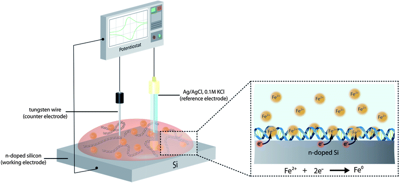 | ||
| Fig. 1 Illustration depicting the electrochemical approach used for the production of the DNA-templated Fe nanowires. An aqueous solution containing λ-DNA and Fe2+ cations is deposited upon an n-doped Si wafer, modified with a TMS SAM, which acts as the working electrode during the electrochemical reduction of the Fe2+ to zerovalent Fe. The DNA acts as a template, facilitating anisotropic growth of the Fe, as a result of the Fe2+ cations associating with the polyanionic DNA duplex structure in solution prior to their reduction. During the electrochemical process, a Ag/AgCl, 0.1 M KCl electrode was used as the reference electrode, and a tungsten wire as the counter electrode. Following nanowire formation, the reaction solution was removed from the Si working electrode, and from which the product material could then be isolated. | ||
The process of nanowire formation can be considered to take place via two distinct stages: the first of these involves association of the Fe2+ cations with the DNA molecules. This plays a key role in the fabrication process, promoting the subsequent formation of the Fe material to take place upon the template. The second stage is the electrochemical reduction of the DNA-bound Fe2+cations to zerovalent Fe, which takes place at the surface of the working electrode. This process results in the growth of an Fe coating around the DNA template molecule to give the final the metal nanowire.
Fourier transform infra-red (FTIR) spectroscopy
As mentioned above, this method for Fe growth relies upon initial association of the Fe2+ cations with the DNA prior to their reduction to the zerovalent state. The rich chemical functionality presented by the DNA offers several different types of site for metal ion interaction. Metal ion binding at the polyanionic phosphodiester backbone for example, can take place through the formation of electrostatic interactions involving the hydrating water molecules around the metal ion or through inner-sphere coordinate bonds directly to the DNA phosphate groups. Alternatively, interactions may also take place through coordination of the metal cations to electron donor sites (e.g. ring nitrogen atoms) within the DNA bases.46,47FTIR spectroscopy was used to probe the interactions between the Fe2+ cations and the DNA. Fig. 2 shows the FTIR spectra of samples of DNA before and after treatment in a solution containing Fe2+ cations. Several changes can be noted following treatment with the Fe2+ solution, indicative of interactions between the DNA and Fe2+ species. The P–O/C–O stretches and PO2− symmetric stretches (1071 cm−1 and 1097 cm−1) originating from the phosphodiester backbone show subtle shifts in frequency upon Fe2+ association (1066 cm−1 and 1103 cm−1). These peaks are also observed to show a relative increase in intensity upon metal binding. A more notable shift in the position of the PO2− asymmetric stretch can also be seen (1244 cm−1 → 1205 cm−1) following Fe2+ treatment. The changes seen in these IR-bands indicate interaction of the Fe2+ cations with the DNA phosphodiester backbone. Similar changes in IR-band positions can also be identified in the nucleobase region (1200–1800 cm−1), indicating the Fe2+ cations also interact with the DNA through coordination to the nucleobases, see ESI.†48
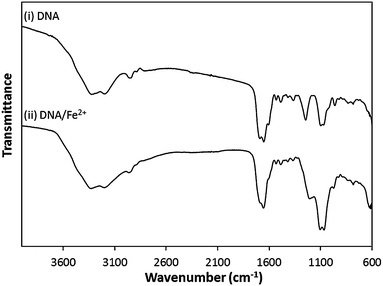 | ||
| Fig. 2 FTIR spectra of (i) “bare” DNA and (ii) DNA following exposure to an aqueous solution of FeSO4 (1 mM). | ||
Cyclic voltammetry
Electrochemical reduction of the DNA-bound Fe2+ species was carried out via a CV approach, adopting the experimental setup previously described, see Fig. 1. A typical voltammogram produced during the nanowire preparation process is shown in Fig. 3. It is characterised by the presence of a single wave, with a cathodic peak potential of E = −1.4 V. This indicates a single irreversible reductive process to be taking place, corresponding to the two-electron reduction of the Fe2+ cations at the n-Si〈100〉 wafer surface.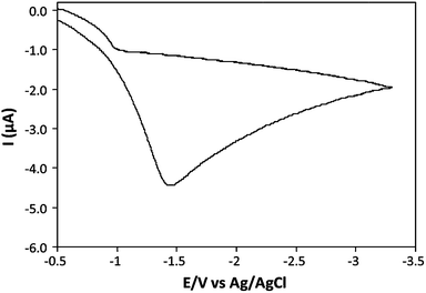 | ||
| Fig. 3 Cyclic voltammogram of the reduction of Fe2+ in a FeSO4 (1 mM)/CT-DNA (500 μg mL−1) aqueous solution at an n-Si〈100〉 electrode. | ||
X-ray diffraction
In order to verify the chemical identity of the material produced during the CV experiments, XRD analysis was performed. To ensure sufficient material was present in the samples to acquire a diffraction pattern, the sample solution was left to dry upon the Si wafer (working electrode) following the electrochemical reaction, and the fabrication process then repeated two further times on the same wafer.The more prominent features in the XRD pattern obtained from the sample (see Fig. 4) are the peaks observed within the 2θ = 10–35° range. These correspond to unreacted starting material (FeSO4) which is present in the sample as a consequence of the manner in which it is required to be prepared in order to obtain meaningful XRD data (i.e. the reaction solution is allowed to dry out upon the substrate support). The presence of FeSO4 within the final product material is simply due to mass transport limitations in solution, which prevent all Fe2+ species being reduced to Fe over the time period which the electrochemical process is carried out.
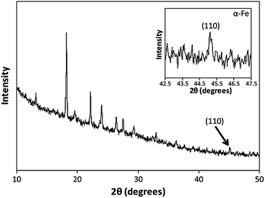 | ||
| Fig. 4 XRD pattern of DNA-templated Fe nanowires, showing the characteristic α-Fe (100) reflection at 2θ = 45°. The series of peaks present at lower 2θ values are attributed to the unreacted FeSO4 starting material present in the sample. | ||
Significantly though, a small peak at 2θ = 45° can also be identified, which is consistent with the (110) reflection of the α-Fe phase (body-centred cubic).49,50 No peaks in the diffraction pattern can be identified which indicate the presence of any iron oxide phases, suggesting the product material is predominantly metallic α-Fe. It should be noted however, (vide infra) that this does not rule out the possibility of the α-Fe possessing an oxide layer at its surface to which XRD is insensitive.
X-ray photoelectron spectroscopy
XPS studies carried out upon the product material not only verified the presence of zerovalent metallic Fe, but also allowed for the surface/core chemical composition of the Fe material to be elucidated through depth profile analysis. Fig. 5a shows a high resolution XP spectrum of the Fe2p region of the product material. The spectrum shows a broad doublet structure with binding energy around Fe2p3/2 = 711.2 eV, and Fe2p1/2 = 724.3 eV. Curve-fitting of the spectrum has not been carried out due to the complex and unreliable nature of accurately assigning Fe2p spectra which potentially contain more than one type of Fe species; as well as requiring to fit each species present, the fit would be further complicated by multiplet splitting of the components due to electrostatic and spin–orbit interactions between the 2p core hole and the unpaired 3d electrons of the photoionised species (characteristic of high-spin Fe2+ and Fe3+ species).51–53 However, despite these complexities, several distinctive features of the spectrum can be identified which allow for different Fe species to be distinguished. Firstly, the measured binding energy of the spectrum (Fe2p3/2 = 711.2 eV) is consistent with the presence of Fe3+ species.53–55 However, the broad nature and overall line shape of the spectrum also suggests a second Fe component to be present. In particular, a broad tail can be seen to the higher binding energy side (∼713 to 717 eV) of the Fe2p3/2 peak, characteristic of a Fe2+ satellite peak.53,54 In addition, the steep shoulder observed on the lower binding energy side of the Fe2p3/2 peak is indicative of an Fe2+ component overlapping with the Fe3+ component at higher binding energy.54 It should also be noted that a shake-up satellite around 719 eV would typically be expected to be seen in the Fe3+ spectrum. However, this cannot be easily distinguished in this case as a result of the overlap with the Fe2+ spectrum.54–56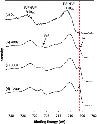 | ||
| Fig. 5 High resolution XPS spectra of the Fe2p region, recorded from a sample of DNA-templated Fe nanowires. The spectra were recorded following etching of the sample material by Ar+ sputtering for (a) 0 s, (b) 400 s, (c) 800 s, and (d) 1200 s, respectively. | ||
The Fe2+ species detected in the sample can be attributed to the presence of FeSO4.53,54 This was further verified by the S2p peak around 168.7 eV, which is consistent with the presence of sulfur in the form of SO42− species,57,58 see ESI.† These findings are in agreement with the XRD data which showed several peaks in the diffraction pattern relating to unreacted FeSO4 due to the manner in which the sample material was prepared.
The presence of Fe3+ is most likely the consequence of surface oxidation of the Fe product material, forming an oxide layer around the Fe metal. The formation of such coatings is generally known to take place at the surface of nanostructured Fe materials, typically in the form of an oxide such as Fe2O3 or Fe3O4, or as oxyhydroxide (FeOOH).59–62 However, the similar binding energies of the Fe2p core level in these two materials, along with the complexities of having multiple components present in the Fe2p envelope, makes it difficult to confirm in which phase the oxide layer is present in this instance.
Another important feature of the spectrum in Fig. 5a is the absence of a doublet peak arising from the zerovalent metallic Fe, expected around 706–708 eV (Fe2p3/2). This confirms there to be no Fe present in the surface layers of the fabricated structures. When it is also considered that the XRD data indicated the product material to be predominantly composed of α-Fe, this suggests that the DNA/Fe structures do indeed possess an iron/oxide core–shell structure. In order to verify this, depth profile XPS analysis was also carried out. Fig. 5 shows a series of XP spectra of the Fe2p region from the DNA/Fe material following etching by Ar+ sputtering for a defined period of time (0–1200 s).
The appearance of an additional doublet at lower binding energy (Fe2p3/2 = 706.9 eV, and Fe2p1/2 = 719.8 eV) relative to the Fe2+/Fe3+ signal is observed in the spectra upon etching, which increases in intensity as a function of the etching time. The binding energy of this doublet is consistent with zerovalent Fe,50,63 confirming that the core of the Fe-based structures are composed of metallic Fe, in agreement with XRD data.¶ Though the DNA/Fe material has been shown to consist of a core–shell structure, for clarity the structures will be referred to as “DNA-templated Fe” from here on.
Atomic force microscopy studies
AFM has been used to evaluate the structure and morphology of individual DNA-templated Fe nanowires formed during the electrochemical process. Nanowires were able to be isolated from the reaction solution through alignment onto a fresh TMS-modified Si substrate via “molecular combing” type processes.31,64Fig. 6a shows an AFM height image of a typical Fe structure aligned upon a TMS-modified Si substrate. The influence of the DNA upon the growth of the electrodeposited Fe is clear with the geometry of the resulting DNA-templated Fe nanostructure retaining the high-aspect ratio dimensions of the template. The Fe appears to form a continuous coating around the DNA with little evidence of gaps in its structure. Upon closer inspection the metal coating can be seen to exhibit a granular morphology (see Fig. 6a, inset), consisting of a linear arrangement of nanoparticles densely packed together along the DNA, i.e. type-(i) structure, Fig. 6b. It cannot be established from the AFM data if these particles are coalesced into a continuous structure or are present as a series of discrete particles, however.|| The morphology associated with the metal coating is most likely a consequence of the Fe formation taking place through a series of nucleation and growth processes on the template, similar to that previously reported in the preparation of other DNA-templated metal structures.26,28,30,33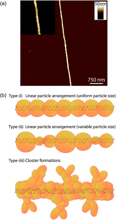 | ||
| Fig. 6 (a) TappingMode™ AFM height image of a DNA-templated Fe nanowire. The inset image shows a zoomed-in region of the nanowire with the image contrast adjusted to highlight the nanowire morphology, which consists of linear arrangements of metal particles packed along the DNA template. (b) Illustrations showing (i) the morphology exhibited by the current DNA-templated Fe nanowires, and (ii and iii) the two general morphology types that have previously been reported following the preparation of various DNA-templated nanowires. | ||
It can also be noted from the nanowire shown in Fig. 6a that the constituent Fe nanoparticles of the metal coating appear highly monodisperse in size. This is in contrast to morphologies seen in previously reported examples of DNA-templated nanostructures, which have typically displayed one of two general types of structure. The first of these can be described as linear arrangements of nanoparticles along the DNA, similar to that shown by the current DNA-templated Fe nanowires, but with greater variation in the constituent particle sizes (type-(ii) structure, Fig. 6b).31,33,38 This variation is proposed to be the result of a progressive nucleation process by which the material growth takes place on the DNA. The second morphology type involves the templated material binding in a much less linear fashion, forming clusters of particles around the DNA, which in some instances produce structures with a dendritic appearance26,29,30 (type-(iii) structure, Fig. 6b). Such structures, which are similar to the well-known diffusion-limited aggregation structures,65,66 arise from a lack of reversibility in the deposition process and the absence of surface tension effects.67 In the case of the DNA-templated Fe nanowires described here, we suggest two factors which may be responsible for the uniform particle growth seen: (a) the electrochemical experiment induces instantaneous nucleation on the template favouring a more uniform particle size compared to progressive nucleation which leads to type-(ii) structures; (b) confinement of nuclei to a 1-D template results in inhibition of the growth of larger particles because they experience overlap with their neighbours sooner. Both factors are likely to narrow the size distributions of particles nucleating and growing on DNA in comparison with the cases of nucleation at a surface or in a bulk phase. These effects are the subject of more detailed theoretical work, which can be found elsewhere.68
Whilst there is a relatively narrow size distribution of the constituent particles associated with any individual nanowire, AFM analysis revealed considerably more variation in the mean diameters between different nanowires in the product material; height measurements showed the nanowires to range in size from 2–26 nm in diameter.
Scanned conductance microscopy
In order to establish that the DNA-templated Fe structures are conducting, i.e. genuine nanowires, SCM has been used, which provides a convenient, qualitative, means of assessing the electrical properties.25,69,70Fig. 7a shows an SCM phase image of two DNA-templated Fe nanowires recorded at an applied bias of +7 V, along with the accompanying AFM height image (Fig. 7b). Information relating to the electrical behaviour of such structures can be elucidated from the phase contrast associated with them in the phase images. Specifically, negative/dark contrast is observed if the nanostructure is electrically conducting, whilst dielectric structures produce only positive/bright contrast.25,69,70 It is clear that the DNA-templated Fe nanowires shown in the AFM height image correspond to the prominent negative/dark contrast seen in the phase image. This was found to be the case over the range of bias potentials used (between −7 V and +7 V), confirming that the structures are electrically conductive. The magnitude of the phase shifts associated with the nanowires (relative to the substrate background) were dependent upon the applied bias, as can be seen by the parabolic trend displayed when plotting the tangent of the phase shifts as a function of the applied bias (Fig. 7c). This relationship between the phase shifts and applied bias is characteristic of the probe–sample interactions being dominated by capacitance effects rather than electrostatic interactions, which are expected to show a linear relation.70–73 This confirmation that the phase shifts are predominantly influenced by the tip/substrate capacitance, rather the presence of static charges on the wire, verifies that the negative phase shift is indicative of the conductive nature of the nanowire.70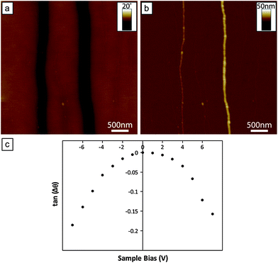 | ||
| Fig. 7 (a) SCM phase image of DNA-templated Fe nanowires supported upon a n-Si〈100〉/200 nm SiO2 wafer, recorded at an applied bias potential of +7 V. The negative phase contrast associated with the nanowires is indicative of structures which are electrically conductive. (b) The corresponding AFM height image of the nanowires featured in (a). The mean diameters of the two nanowires present in the image are 4.7 nm (left) and 12.0 nm (right), respectively. (c) Plot of the tangent of the nanowire phase shifts (measured from the 12.0 nm diameter wire) against the bias potential applied to the sample. The parabolic relationship observed indicates capacitance effects of the conductive wire dominate the probe–sample interactions. | ||
Although the SCM data presented cannot be used to derive the actual conductivity of the nanowires, the technique is very sensitive to low conductivities. The observation of a negative phase shift in the SCM images indicates a lower bound on the conductivity of the order of 10−14 S cm−1, using a calculation analogous to that described by Bockrath et al.69 and taking account of the tapping frequency of the tip.
Magnetic force microscopy
Zerovalent Fe, when in bulk form, is one of the best known examples of a ferromagnetic material. However, magnetic properties are known to be size-dependent,74,75 which can lead to nanomaterials exhibiting quite different magnetic properties compared to the corresponding bulk form. An example of this is the transition from a bulk ferromagnetic to superparamagnetic behaviour when in nanoparticle form, where the particle volume is smaller than the size of a single magnetic domain.74,75 This change is a consequence of the magnetic anisotropy energy being overcome by the thermal energy, and results in randomisation of the magnetic spin direction, leading to a net magnetisation of zero in the absence of any external magnetic field. The geometry of nanostructured materials also plays an important role in determining magnetic character due its high sensitivity towards anisotropic effects.76,77 Hence the nanostructured form in which a material is prepared (e.g. nanoparticles, nanowires/nanorods) can also dictate magnetic character. It was therefore of interest to probe the magnetic behaviour of the Fe structures produced here. In order to achieve this, magnetic force microscopy (MFM) was used. MFM operates in a highly analogous fashion to the SCM technique though in this instance a magnetised AFM probe is used and its response to the magnetic force gradients are monitored as it scans over the sample (cf. the electric force gradients monitored during SCM experiments).36Fig. 8a shows an MFM phase image of a DNA-templated Fe nanowire recorded at a lift height of 18 nm, along with the corresponding height image (Fig. 8b). The position of the nanowire can be clearly seen to correspond to a region of dark contrast in the MFM phase image, indicating the Fe structure to exhibit a room temperature magnetic response to the probe. In addition, the dark contrast indicates that the magnetic interaction between the probe and nanowire is an attractive one, i.e. the magnetic moments of the nanowire and probe are in alignment with one another. The phase signal was found to persist over a range of lift heights, gradually diminishing as the probe–sample separation was increased, see Fig. 8c.
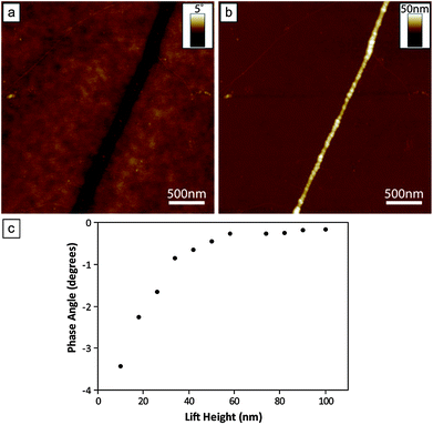 | ||
| Fig. 8 (a) MFM phase image of a DNA-templated nanowire supported upon a n-Si〈100〉/200 nm SiO2 wafer, recorded with the magnetised AFM probe maintained at a lift height of 18 nm. The negative contrast associated with the nanowire indicates attractive magnetic interactions between the structure and the probe. (b) The corresponding AFM height image of nanowire shown in (a). The mean diameter was the nanowire is 17.4 nm. (c) Plot showing the magnitude of the measured nanowire phase shifts as a function of the lift height of the probe. | ||
It is should be noted here that despite the similarities between the MFM and SCM techniques, the phase shifts observed here are able to be distinguished as arising from magnetic interactions between the tip and sample, rather than electrostatic effects. In the previous SCM experiments, phase shifts associated with the nanowires at zero bias were observed to be less than 0.05°, at a lift height of 70 nm (see Fig. 7c). In comparison, the phase signal observed in MFM experiments (which are carried out in the absence of an applied bias), at the same lift height, is substantially larger, at around 0.3° (see Fig. 8c). In addition, the same type of AFM tip (metallic Co/Cr coated n-doped silicon) is used in both SCM and MFM experiments; it can be noted that an electrostatic signal is only observed upon application of a dc bias, whilst a magnetic-based phase response can only be identified when the tip has been magnetized. These observations rule out the MFM phase signals arising as a result of electrostatic effects.
Control experiments were also carried out using non-magnetic Si probes, in which no contrast was seen in the resulting phase images. This again confirms that the phase signals observed are the result of magnetic interactions between the magnetised tip and nanowire.
In order to establish the type of magnetic behaviour displayed by the nanowire, additional MFM experiments were performed in which the direction of the probe's magnetisation was reversed. If the Fe nanowire is ferromagnetic in character (as Fe is in its bulk form) reversing the direction of the probe's magnetisation would be expected to result in the phase signal inverting, i.e. changing from dark contrast to bright contrast, as any probe–nanowire interactions will now be repulsive. However, the dark phase contrast associated with the nanowire was found to persist regardless of the direction of the probe's magnetisation. This behaviour is consistent with the magnetic field of the AFM probe inducing alignment of the magnetic moments within the region of the nanowire over which the probe is positioned at any given time, indicating that the nanowire structure is composed of a series of superparamagnetic Fe particles packed along the DNA template. The proposed structure here is also supported by the morphology of the nanowires, i.e. linear arrangements of Fe nanoparticles, densely packed along the DNA. This finding is similar to that which we recently reported for DNA-templated magnetite (Fe3O4) nanowires, where superparamagnetism was displayed in contrast to the ferrimagnetism observed in the bulk phase.36
Conclusions
For the first time, an electrochemical approach has been demonstrated as a part of a DNA-templating method for the fabrication of magnetic nanowires. The directed growth of the zerovalent Fe produced during the electrochemical reduction process arises from binding to the DNA template, allowing for high aspect ratio nanowires to be formed with diameters up to ∼26 nm. The chemical composition of the nanostructures was determined to consist of a core–shell structure, where an oxide sheath encapsulates the Fe core. The extension of electrochemical methods to DNA-templating3 may offer access to new nanostructured materials such as those not otherwise readily compatible with the typical conditions of chemical routes (e.g. Bi2O3)37 as well as possibly offering an effective means of modifying surface-based template structures for device fabrication.Materials and methods
Materials
All chemicals, unless otherwise stated, were purchased from Sigma-Aldrich Company Ltd., of Analar grade or equivalent, and used as received. Ferrous sulfate heptahydrate (FeSO4·7H2O, 99%) was obtained from BDH Chemicals Ltd. Lambda DNA (λ-DNA, Cat no. N3011S) was purchased from New England Biolabs (UK) Ltd. Calf thymus DNA (CT-DNA, highly polymerised, 6% sodium) was purchased from Sigma-Aldrich Company Ltd. and used as received. n-Si〈100〉 wafers (3 inch diameter, 525 ± 50 μm thickness, polished on one side with reverse etched, phosphorus doped, 1–10 Ω cm resistance) were used as the working electrode in electrochemistry experiments and as substrate supports for AFM imaging of samples. n-Si〈100〉 wafers with a thermally grown SiO2 layer on top (3 inch diameter, 500 ± 25 μm, double side polished, arsenic doped, <0.005 Ω cm resistance, thermal oxide layer 2000 Å ± 10% thickness) were used in scanned conductance microscopy (SCM) and magnetic force microscopy (MFM) experiments. All Si wafers were purchased from Compart Technology Ltd.NANOpure® deionised water (18 M Ω cm resistivity) was obtained from a NANOpure® DIamond™ Life Science ultrapure water system equipped with a DIamond™ RO Reverse Osmosis System (Barnstead International).
Cleaning and oxidation of Si substrates
n-Si〈100〉 wafers were cut into ∼1 × 1 cm2 pieces using a diamond scribe, and treated in “Piranha” solution (4![[thin space (1/6-em)]](https://www.rsc.org/images/entities/char_2009.gif) :1 H2SO4–H2O2) for 45 minutes (Caution! Piranha solution should be handled with extreme care; it is a strong oxidant and reacts violently with many organic materials. It also presents an explosion danger). Upon removal from the Piranha solution, the Si wafers were rinsed with copious amounts of NANOpure® water, and dried in a gentle stream of N2(g) before further drying in an oven for 5–10 minutes.
:1 H2SO4–H2O2) for 45 minutes (Caution! Piranha solution should be handled with extreme care; it is a strong oxidant and reacts violently with many organic materials. It also presents an explosion danger). Upon removal from the Piranha solution, the Si wafers were rinsed with copious amounts of NANOpure® water, and dried in a gentle stream of N2(g) before further drying in an oven for 5–10 minutes.
For n-Si〈100〉/200 nm SiO2 wafers used in SCM and MFM experiments, the thermally grown SiO2 layer was removed from one side of the wafer prior to Piranha treatment. This was carried out through applying a drop of HF solution (48% in H2O) onto the surface of the Si wafer, and left until a change in the surface wetting was observed (i.e. hydrophilic to hydrophobic transition), indicated by a sudden “beading” of the HF solution. The HF solution was removed from the wafer, which was subsequently rinsed with copious amounts of NANOpure® water, followed by treatment in Piranha solution as previously described.
Trimethylsilane modification of Si substrates
Unless otherwise stated, all Si wafers (n-Si〈100〉 and n-Si〈100〉/200 nm SiO2 wafers) were modified with a self-assembled monolayer of trimethylsilane (TMS) prior to use. TMS modification was performed through vapour treatment with Me3SiCl. This was carried out by placing a specimen bottle containing 100 μL of Me3SiCl inside a larger specimen bottle. The Piranha-treated Si wafer was placed on the top of the inner specimen bottle (polished/SiO2 side facing up) and left for 10 minutes at room temperature. TMS modification results in an increase in the hydrophobic character of the substrate surface. Under the conditions employed here, static contact angle measurements typically give values of ∼71° (NANOpure® water as the probe liquid).24Fourier transform infra-red spectroscopy of DNA/Fe2+
All samples for FTIR spectroscopy were prepared as films upon Si wafers in order to ensure sufficient material was present to obtain useful data. Prior to preparation of the samples, the Si wafers were treated with Piranha solution as previously described, but were not subject to TMS modification.Samples of bare DNA (i.e. prior to exposure to the Fe2+ solution) were prepared by depositing 80 μL of an aqueous solution of CT-DNA (1 mg mL−1) upon a n-Si〈100〉 wafer and allowing the solvent to evaporate at room temperature. Samples of DNA/Fe2+ were prepared by adding 60 μL of an aqueous solution of FeSO4·7H2O (1 mM) to 30 μL of an aqueous solution of CT-DNA (1 mg mL−1), and left to stand for 10 minutes. 80 μL of the resulting DNA/Fe2+ solution was deposited upon a n-Si〈100〉 wafer, and the solvent allowed to evaporate at room temperature. FTIR spectra were acquired using a Bio-Rad Excalibur FTS-40 spectrometer (Varian Inc.). Spectra were recorded in the range 400–4000 cm−1, with 128 scans at 4 cm−1 resolution. The spectra shown have been offset and scaled for clarity.
Preparation of DNA/Fe material for X-ray diffraction and X-ray photoelectron spectroscopy studies
The DNA/Fe material for X-ray diffraction (XRD) and X-ray photoelectron spectroscopy (XPS) was required to be prepared in a manner which ensured sufficient product material could be obtained to allow for meaningful data to be acquired. Samples were prepared by adding 200 μL of an aqueous solution of FeSO4·7H2O (1 mM) to 100 μL of an aqueous solution of CT-DNA (500 μg mL−1) and leaving to stand for 10 minutes. 40 μL of the resulting DNA/Fe2+ reaction solution was then drop-cast onto a TMS-modified n-Si〈100〉 substrate for electrochemical reduction of the Fe2+ species to be carried out. The electrochemical process was carried out via a cyclic voltammetry (CV) approach, in which the TMS-modified n-Si〈100〉 substrate was used as the working electrode, and the counter and reference electrodes were tungsten wire (diameter = 0.25 mm) and Ag/AgCl bridged by a saturated KCl (0.1 M) solution, respectively. The hydrophobic nature of the TMS-modified substrate results in “beading” of the deposited DNA/Fe2+ solution, enabling the counter and reference electrodes to be easily inserted into the solution droplet without contacting substrate surface. CV measurements, and electrochemical reduction of the Fe2+, was performed using a computer-interfaced SECM CHI 900 electrochemical microscope system (CH Instruments), sweeping the potential between E = +0.3 V and E = −3.3 V, with a scan rate of v = 0.1 V s−1, quiet time of t = 2.0 seconds, and sweep segments = 2. Following the electrochemical process, the reaction solution was allowed to dry upon the working electrode at room temperature in order to maximise the amount of product material present for subsequent analysis. In the case of samples prepared for XRD, this procedure was repeated a further two times on the same Si substrate in order to provide sufficient of the product material for a diffraction pattern to be acquired.Preparation and alignment of DNA-templated Fe nanowires for scanning probe microscopy studies
Whilst CT-DNA was used in the preparation of the DNA-templated Fe where large amounts of material were required for investigation (FTIR, XRD, XPS), λ-DNA was employed as the templating agent in the preparation of Fe nanowires fabricated for SPM studies. Molecules of λ-DNA are of a consistent length (16.2 μm), allowing for the formation of well-defined nanowire structures, highly suited for investigation by SPM.Samples were prepared by adding 10 μL of an aqueous solution of FeSO4·7H2O (1 mM) to 5 μL of an aqueous solution of λ-DNA (500 μg mL−1), which was left to stand for 10 minutes. 5 μL of the DNA/Fe2+solution was deposited upon a TMS-modified n-Si〈100〉 wafer. CV was subsequently carried out at the surface of the wafer as previously described. Following the electrochemical process, the reaction solution, containing the newly formed DNA-templated Fe nanowires, was removed from the Si working electrode by micropipette. The nanowires were then isolated from the reaction solution by immobilisation upon a fresh TMS-modified n-Si〈100〉 wafer, using a process loosely based upon spin-coating methods: the DNA/Fe solution was applied to a TMS-modified n-Si〈100〉 wafer whilst spun at 125 rpm. The substrate was spun for a further 2 minutes at 250 rpm before the residual solution was withdrawn from the substrate surface by micropipette. This procedure results in the nanowires being stretched out across the substrate surface, as directed by the action of the receding meniscus of the solution droplet as it withdraws from the surface.
X-ray diffraction
XRD data was acquired using of a PANalytical X'Pert Pro diffractometer (PANalytical) using Cu Kα radiation source (λ = 1.540Å).X-ray photoelectron spectroscopy
XPS was carried out using a Thermo Scientific K-Alpha X-ray photoelectron spectrometer (Thermo Electron Corp., East Grinstead, UK), equipped with an Al Kα X-ray source (1486.6 eV) with a variable spot size of 30–400 μm. A take-off angle of 90° was used during data acquisition, and a charge neutralisation gun used to compensate for surface charging. All spectra were referenced to hydrocarbon C1s peak at 285.0 eV. Survey spectra were acquired using a pass energy of 150 eV, whilst high resolution region spectra were acquired using a pass energy of 50 eV. For depth profiling experiments, an Ar+ ion gun (200 eV) was used for sputter etching of samples. Data analysis was carried out using CasaXPS software (Casa Software Ltd.). The Fe2p spectra shown have been offset and scaled for clarity.Atomic force microscopy
AFM data was acquired using Multimode Nanoscope IIIa and Dimension Nanoscope V AFM systems (Veeco Instruments Inc., Metrology Group). Both were operated in TappingMode™, using TESP (n-doped Si cantilevers, resonant frequency range = 230–410 kHz, force constant range = 20–80 N m−1) (Veeco Instruments Inc., Metrology Group) and Tap300Al-G (Si cantilevers, resonant frequency range = 200–400 kHz, force constant range = 20–75 N m−1) (BudgetSensors) model AFM probes. Data acquisition was carried out using Nanoscope versions 5.12b36, and 7.00b19 software (Veeco Instruments Inc., Digital Instruments) for the Multimode IIIa and Dimension V systems, respectively. For decreasing vibrational noise an isolation table/acoustic enclosure was used (Veeco Inc., Metrology Group).Scanned conductance microscopy (SCM) and magnetic force microscopy (MFM)
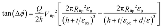
SCM is a variant of electric force microscopy (EFM) in which the force gradient above the sample is mapped; a dc potential bias is applied between the sample and the tip, and the phase angle between the driving force applied to the cantilever and the tip response is monitored. This technique has been called scanned conductance microscopy because conductive objects on a dielectric film modify the capacitance between the tip and the substrate in a manner distinct from that due to polarisable insulators.69,70,78 SCM is implemented as a two-pass technique in which the first scan across a line records the topography in TappingMode™ operation, and this information is used to lift the tip a defined height above the sample in the second pass to record the phase response.The electrostatic force is negligible compared to the short range forces in the first pass, but the electrostatic force dominates in the second pass.79 As shown by previous workers,69,70 negative phase shifts (with respect to the background) are only observed when imaging structures that are conductive. The phase shift is proportional to the second derivative of the tip/surface capacitance with respect to the lift height because ∂2E/∂z2, where E is the energy stored in the capacitance and z is the coordinate normal to the surface, is equivalent to a change in the spring constant of the cantilever. The capacitance is the series combination of the tip/nanowire and nanowire/surface capacitors. The phase shift, Δϕ, for an insulating object may be estimated using a model geometry in which the nanowire is represented by the area of a thin dielectric strip directly under the tip, itself modelled as a disc of radius, Rtip:70
 | (1) |
Quantitative calculations of the phase shift as a function of nanowire length have been previously been described by others;69,70 in this work we use the method in a qualitative fashion to demonstrate the conductive nature of our nanowires. EFM provides a complementary way to image conductance in a convenient contactless imaging experiment.
The MFM technique operates in an analogous manner to EFM; in this case a magnetised AFM tip is used which allows for the magnetic force gradients above a sample to be mapped through monitoring the phase response of the tip during its second pass over each scan line.
SCM and MFM data was acquired with a Dimension Nanoscope V system, using MESP (metallic Co/Cr coated n-doped silicon cantilevers, resonant frequency range = 60–100 kHz, spring constant range = 1–5 N m−1) model AFM probes (Veeco Instruments Inc., Metrology Group). Data acquisition was carried out with the use of Nanoscope Version 7.00b19 software (Veeco Instruments Inc., Digital Instruments). Vibrational noise was again reduced using an isolation table/acoustic enclosure.
Both SCM and MFM measurements were conducted using the “two-pass” approach described earlier, with lift heights in the range of 40–100 nm (SCM) and 10–100 nm (MFM) used during the second pass of the tip over each scan line. A scan rate of 0.5 Hz was employed during data acquisition in both SCM and MFM experiments.
During SCM measurements an electrostatic field was generated between the probe and sample using an independently controlled direct current (dc) bias applied to the sample, while the probe was grounded. SCM experiments typically involved a series of phase images of the same sample area being acquired at a range of different of dc bias potentials (between −7 and +7 V), whilst keeping the lift height constant.
Immediately prior to MFM measurements, the MESP probes were magnetised using a permanent magnet for ∼2 minutes. MFM experiments typically involved recording a series of phase images of the same sample area, at a range of different lift heights.
Acknowledgements
The National EPSRC XPS User's Service (NEXUS), at Newcastle University, Newcastle-Upon-Tyne, UK is acknowledged for technical assistance with XPS. This work was financially supported by One North East, EU-FP7 project LAMAND (Contract no. 245565), Newcastle University, Azzaytuna University, Tarhuna, Libya, and the Libyan Government.Notes and references
- G. A. Ozin and A. C. Arsenault, Nanochemistry: A Chemical Approach to Nanomaterials, Royal Society of Chemistry, Cambridge, 2005 Search PubMed.
- The Chemistry of Nanomaterials. Synthesis Properties and Applications, ed. C. N. R. Rao, A. Müller and A. K. Cheetham, Wiley-VCH, Weinheim, 2004 Search PubMed.
- A. Houlton and S. M. D. Watson, Annu. Rep. Prog. Chem., Sect. A: Inorg. Chem., 2011, 107, 21–42 RSC.
- Y. Xia, P. Yang, Y. Sun, Y. Wu, B. Mayers, B. Gates, Y. Yin, F. Kim and H. Yan, Adv. Mater., 2003, 15, 353–389 CrossRef CAS.
- D. Borissov, S. Isik-Uppenkamp and M. Rohwerder, J. Phys. Chem. C, 2009, 113, 3133–3138 CAS.
- M.-M. Song, W.-J. Song, H. Bi, J. Wang, W.-L. Wu, J. Sun and M. Yu, Biomaterials, 2010, 31, 1509–1517 CrossRef CAS.
- Q. Wang, G. Wang, B. Xu, J. Jie, X. Han, G. Li, Q. Li and J. G. Hou, Mater. Lett., 2005, 59, 1378–1382 CrossRef CAS.
- J. Verbeeck, O. I. Lebedev, G. Van Tendeloo, L. Cagnon, C. Bougerol and G. Tourillon, J. Electrochem. Soc., 2003, 150, E468–E471 CrossRef CAS.
- T. M. Whitney, J. S. Jiang, P. C. Searson and C. L. Chien, Science, 1993, 261, 1316–1319 CAS.
- D. Wang, H. P. Jakobson, R. Kou, J. Tang, R. Z. Fineman, D. Yu and Y. Lu, Chem. Mater., 2006, 18, 4231–4237 CrossRef CAS.
- D. Wang, H. Luo, R. Kou, M. P. Gil, S. Xiao, V. O. Golub, Z. Yang, C. J. Brinker and Y. Lu, Angew. Chem., Int. Ed., 2004, 43, 6169–6173 CrossRef CAS.
- Y. Cao and T. E. Mallouk, Chem. Mater., 2008, 20, 5260–5265 CrossRef CAS.
- C. R. Martin, Chem. Mater., 1996, 8, 1739–1746 CrossRef CAS.
- S. J. Hurst, E. K. Payne, L. Qin and C. A. Mirkin, Angew. Chem., Int. Ed., 2006, 45, 2672–2692 CrossRef CAS.
- J. Wang, Y. L. Bunimovich, G. Sui, S. Savvas, J. Wang, Y. Guo, J. R. Heath and H.-R. Tseng, Chem. Commun., 2006, 3075–3077 RSC.
- M. A. Bangar, K. Ramanathan, M. Yun, C. Lee, C. Hangarter and N. V. Myung, Chem. Mater., 2004, 16, 4955–4959 CrossRef CAS.
- K. Ramanathan, M. A. Bangar, M. Yun, W. Chen, A. Mulchandani and N. V. Myung, Nano Lett., 2004, 4, 1237–1239 CrossRef CAS.
- Y. Hu, A. C. To and M. Yun, Nanotechnology, 2009, 20, 285605 CrossRef CAS.
- W. Shi, P. Liang, D. Ge, J. Wang and Q. Zhang, Chem. Commun., 2007, 2414–2416 RSC.
- Y. Ma, J. Zhang, G. Zhang and H. He, J. Am. Chem. Soc., 2004, 126, 7097–7101 CrossRef CAS.
- L. Dong, T. Hollis, S. Fishwick, B. A. Connolly, N. G. Wright, B. R. Horrocks and A. Houlton, Chem.–Eur. J., 2007, 13, 822–828 CrossRef CAS.
- J. Hannant, J. H. Hedley, J. Pate, A. Walli, S. A. Farha Al-Said, M. A. Galindo, B. A. Connolly, B. R. Horrocks, A. Houlton and A. R. Pike, Chem. Commun., 2010, 46, 5870–5872 RSC.
- R. Hassanien, M. Al-Hinai, S. A. Farha Al-Said, R. Little, L. Šiller, N. G. Wright, A. Houlton and B. R. Horrocks, ACS Nano, 2010, 4, 2149–2159 CrossRef CAS.
- S. M. D. Watson, J. H. Hedley, M. A. Galindo, S. A. Farha Al-Said, N. G. Wright, B. A. Connolly, B. R. Horrocks and A. Houlton, Chem.–Eur. J., 2012, 18, 12008–12019 CrossRef CAS.
- S. Pruneanu, S. A. Farha Al-Said, L. Dong, T. A. Hollis, M. A. Galindo, N. G. Wright, A. Houlton and B. R. Horrocks, Adv. Funct. Mater., 2008, 18, 2444–2454 CrossRef CAS.
- E. Braun, Y. Eichen, U. Sivan and G. Ben-Yoseph, Nature, 1998, 391, 775–778 CrossRef CAS.
- K. Keren, M. Krueger, R. Gilad, G. Ben-Yoseph, U. Sivan and E. Braun, Science, 2002, 297, 72–75 CrossRef CAS.
- W. E. Ford, O. Harnack, A. Yasuda and J. M. Wessels, Adv. Mater., 2001, 13, 1793–1797 CrossRef CAS.
- J. Richter, R. Seidel, R. Kirsch, M. Mertig, W. Pompe, J. Plaschke and H. K. Schackert, Adv. Mater., 2000, 12, 507–510 CrossRef CAS.
- J. Richter, M. Mertig, W. Pompe, I. Mönch and H. K. Schackert, Appl. Phys. Lett., 2001, 78, 536–538 CrossRef CAS.
- Z. X. Deng and C. D. Mao, Nano Lett., 2003, 3, 1545–1548 CrossRef CAS.
- C. F. Monson and A. T. Woolley, Nano Lett., 2003, 3, 359–363 CrossRef CAS.
- S. M. D. Watson, N. G. Wright, B. R. Horrocks and A. Houlton, Langmuir, 2010, 26, 2068–2075 CrossRef CAS.
- R. Hassanien, S. A. Farha Al-Said, L. Šiller, R. Little, N. G. Wright, A. Houlton and B. R. Horrocks, Nanotechnology, 2012, 23, 075601 CrossRef.
- D. Sarkar and M. Mandal, J. Phys. Chem. C, 2012, 116, 3227–3234 CAS.
- H. D. A. Mohamed, S. M. D. Watson, B. R. Horrocks and A. Houlton, Nanoscale, 2012, 4, 5936–5945 RSC.
- M. G. Hale, R. Little, M. A. Salem, J. H. Hedley, B. R. Horrocks and L. Šiller, Thin Solid Films, 2012, 520, 7044–7048 CrossRef CAS.
- L. Dong, T. Hollis, B. A. Connolly, N. G. Wright, B. R. Horrocks and A. Houlton, Adv. Mater., 2007, 19, 1748–1751 CrossRef CAS.
- W. U. Dittmer and F. C. Simmel, Appl. Phys. Lett., 2004, 85, 633–635 CrossRef CAS.
- D. S. Hopkins, D. Pekker, P. M. Goldbart and A. Bezryadin, Science, 2005, 308, 1762–1765 CrossRef CAS.
- L. Vayssieres, L. Rabenberg and A. Manthiram, Nano Lett., 2002, 2, 1393–1395 CrossRef CAS.
- S. C. Tsang, V. Caps, I. Paraskevas, D. Chadwick and D. Thompsett, Angew. Chem., Int. Ed., 2004, 43, 5645–5649 CrossRef CAS.
- D. L. Huber, Small, 2005, 1, 482–501 CrossRef CAS.
- L. Mohaddes-Ardabili, H. Zheng, S. B. Ogale, B. Hannoyer, W. Tian, J. Wang, S. E. Lofland, S. R. Shinde, T. Zhao, Y. Jia, L. Salamanca-Riba, D. G. Schlom, M. Wuttig and R. Ramesh, Nat. Mater., 2004, 3, 533–538 CrossRef CAS.
- J. M. Kinsella and A. Ivanisevic, Langmuir, 2007, 23, 3886–3890 CrossRef CAS.
- Nucleic Acid – Metal Ion Interactions, ed. T. Spiro, John Wiley & Sons, New York, 1980 Search PubMed.
- G. L. Eichhorn and Y. A. Shin, J. Am. Chem. Soc., 1968, 90, 7323–7328 CrossRef CAS.
- L. Berti and G. A. Burley, Nat. Nanotechnol., 2008, 3, 81–87 CrossRef CAS.
- V. G. Pol, M. Motiei, A. Gedanken, J. Calderon-Moreno and Y. Mastai, Chem. Mater., 2003, 15, 1378–1384 CrossRef CAS.
- K.-C. Huang and S. H. Ehrman, Langmuir, 2007, 23, 1419–1426 CrossRef CAS.
- R. P. Gupta and S. K. Sen, Phys. Rev. B: Solid State, 1975, 12, 15–19 CrossRef CAS.
- N. S. McIntyre and D. G. Zetaruk, Anal. Chem., 1977, 49, 1521–1529 CrossRef CAS.
- A. P. Grosvenor, B. A. Kobe, M. C. Biesinger and N. S. McIntyre, Surf. Interface Anal., 2004, 36, 1564–1574 CrossRef CAS.
- A. T. Kozakov, A. G. Kochur, K. A. Googlev, A. V. Nikolsky, I. P. Raevski, V. G. Smotrakov and V. V. Yeremkin, J. Electron Spectrosc. Relat. Phenom., 2011, 184, 16–23 CrossRef CAS.
- T. Fujii, F. M. F. de Groot, G. A. Sawatzky, F. C. Voogt, T. Hibma and K. Okada, Phys. Rev. B: Condens. Matter Mater. Phys., 1999, 59, 3195–3202 CrossRef CAS.
- T. J. Daou, S. Begin-Colin, J. M. Grenèche, F. Thomas, A. Derory, P. Bernhardt, P. Legaré and G. Pourroy, Chem. Mater., 2007, 19, 4494–4505 CrossRef CAS.
- B. J. Lindberg, K. Hamrin, G. Johansson, U. Gelius, A. Fahlman, C. Nordling and K. Siegbahn, Phys. Scr., 1970, 1, 286–298 CrossRef CAS.
- R. V. Siriwardane and J. M. Cook, J. Colloid Interface Sci., 1985, 104, 250–257 CrossRef CAS.
- X.-Q. Li and W.-X. Zhang, J. Phys. Chem. C, 2007, 111, 6939–6946 CAS.
- X.-Q. Li and W.-X. Zhang, Langmuir, 2006, 22, 4638–4642 CrossRef CAS.
- A. P. Grosvenor, B. A. Kobe and N. S. McIntyre, Surf. Sci., 2004, 572, 217–227 CrossRef CAS.
- C. Wang, D. R. Baer, J. E. Amonette, M. H. Engelhard, J. Antony and Y. Qiang, J. Am. Chem. Soc., 2009, 131, 8824–8832 CrossRef CAS.
- P. Mills and J. L. Sullivan, J. Phys. D: Appl. Phys., 1983, 16, 723–732 CrossRef CAS.
- J. Li, C. Bai, C. Wang, C. Zhu, Z. Lin, Q. Li and E. Cao, Nucleic Acids Res., 1998, 26, 4785–4786 CrossRef CAS.
- T. A. Witten and L. M. Sander, Phys. Rev. Lett., 1981, 47, 1400–1403 CrossRef CAS.
- P. Meakin, Phys. Rev. Lett., 1983, 51, 1119–1122 CrossRef.
- P. Meakin, Fractals, scaling and growth far from equilibrium, Cambridge University Press, Cambridge, 1998 Search PubMed.
- S. M. D. Watson, A. Houlton and B. R. Horrocks, Nanotechnology, 2012, 23, 505603 CrossRef.
- M. Bockrath, N. Markovic, A. Shepard, M. Tinkham, L. Gurevich, L. P. Kouwenhoven, M. W. Wu and L. L. Sohn, Nano Lett., 2002, 2, 187–190 CrossRef CAS.
- C. Staii, A. T. Johnson and N. J. Pinto, Nano Lett., 2004, 4, 859–862 CrossRef CAS.
- T. S. Jespersen and J. Nygard, Nano Lett., 2005, 5, 1838–1841 CrossRef CAS.
- R. M. Nyffenegger, R. M. Penner and R. Schierle, Appl. Phys. Lett., 1997, 71, 1878–1880 CrossRef CAS.
- B. D. Terris, J. E. Stern, D. Rugar and H. J. Mamin, Phys. Rev. Lett., 1989, 63, 2669–2672 CrossRef CAS.
- Y.-W. Jun, J.-W. Seo and J. Cheon, Acc. Chem. Res., 2008, 41, 179–189 CrossRef CAS.
- M. Colombo, S. Carregal-Romero, M. F. Casula, L. Gutiérrez, M. P. Morales, I. B. Böhm, J. T. Heverhagen, D. Prosperi and W. J. Parak, Chem. Soc. Rev., 2012, 41, 4306–4334 RSC.
- H.-L. Sun, H. Shi, F. Zhao, L. Qi and S. Gao, Chem. Commun., 2005, 4339–4341 RSC.
- Q. Song and Z. J. Zhang, J. Am. Chem. Soc., 2004, 126, 6164–6168 CrossRef CAS.
- Y. Zhou, M. Freitag, J. Hone, C. Staii, A. T. Johnson, N. J. Pinto and A. G. MacDiarmid, Appl. Phys. Lett., 2003, 83, 3800–3802 CrossRef CAS.
- M. Yan and G. H. Bernstein, Surf. Interface Anal., 2007, 39, 354–358 CrossRef CAS.
Footnotes |
| † Electronic supplementary information (ESI) available. See DOI: 10.1039/c3nr00716b |
| ‡ SMDW and HDAM contributed equally to this work. |
| § We have recently reported the growth of the wide band gap material Bi2O3 on DNA using an electrochemical route.37 |
| ¶ It should be noted that the Fe2p signal from the oxide material is still observed following etching, as the sample is not deposited as a homogenous film, and will consist of a multilayer network of DNA-templated Fe nanostructures. |
| || The coalescence of such particles on DNA has recently been modelled and found to be the equilibrium state under appropriate conditions of low material:template stoichiometry.66 |
| This journal is © The Royal Society of Chemistry 2013 |