 Open Access Article
 This Open Access Article is licensed under a
 Creative Commons Attribution 3.0 Unported Licence
Structural and electronic properties of a large-scale Moiré pattern of hexagonal boron nitride on Cu(111) studied with density functional theory†
Ralph
Koitz
*,
Ari P
Seitsonen
,
Marcella
Iannuzzi
and
Jürg
Hutter
Physikalisch-Chemisches Institut, University of Zurich, Winterthurerstrasse 190, 8057 Zurich, Switzerland. E-mail: r.koitz@pci.uzh.ch
First published on 24th April 2013
Abstract
Hexagonal boron nitride (h-BN) adsorbed on metal surfaces shows great promise for applications in nanoscience. Depending on the nature of the substrate, effects such as an extended corrugation of the monolayer can be observed and utilized, e.g. for the patterning of adsorbed molecules. Here we present an in-depth computational study of the structural and electronic properties of a 6 nm Moiré pattern formed by a rotated layer of h-BN on a Cu(111) surface. In contrast to related systems, the h-BN layer undergoes only minute structural changes upon adsorption. Nevertheless, the projected density of states at various atoms in the cell and the electrostatic potential above the surface are periodically modulated, leading to the experimentally observed electronic corrugation. We rationalize this observation with the variation in adsorption registry resulting in periodic changes of the lateral, rather than vertical, h-BN–Cu distances.
1 Introduction
Two-dimensional molecular sheets adsorbed on metallic substrates have received a lot of attention in recent years.1 Such materials have shown promise for applications in nanoscience, particularly for nanoelectronics,2 chemical sensing,3 and as template surfaces for molecular assembly.4,5 Frequently graphene adsorbed on metals is studied in this context, but its isoelectronic analog hexagonal boron nitride (h-BN) exhibits equally interesting and versatile properties. Both the lattice mismatch between h-BN and the substrate surface and the interaction strength have a strong influence on the structural and electronic properties of the adsorption system. Thus h-BN forms the strongly corrugated nanomesh on a Rh(111) surface6 but flat layers on Ni(111) and Cu(111).7As an infinite layer is adsorbed onto a substrate with a sufficiently different lattice constant, the mismatch results in the formation of approximate superstructures with large unit cells.8 In such a system the position of atoms in the overlayer relative to those of the substrate (adsorption registry) is not uniform, but varies periodically. If no buckling or reconstruction of the monolayer occurs, this lateral variation results in a Moiré pattern on the surface, i.e. a two-dimensional array of so-called moirons.8 In addition to the mismatch of lattice constants, a rotation of the layers relative to each other also influences the periodicity of such patterns. An example of a long-range Moiré lattice was reported for graphene on Ru(0001), which forms a 25 × 25 unit cell on a 23 × 23 Ru unit.9 Subsequent Density Functional Theory (DFT) calculations of this system (modelled as a 12-on-11 superstructure) elucidated its structure in great detail.10–12 In particular, it was found that the corrugation observed in scanning tunneling microscopy (STM) experiments originated mainly from a substantial structural buckling of the monolayer, which led to a lateral variation of the graphene electronic structure.
Although so far not exhaustively investigated, Cu(111) is a promising surface for h-BN adsorption. During the last decade, a number of theoretical and experimental studies have been published.7,13,14 Technologically, large-scale growth of h-BN on Cu is important for the mass production of foils used as substrates for graphene-based devices.14,15 Most recently, the h-BN/Cu system was studied in great detail with STM.16 It was found that, although the monolayer is flat and resides at a relatively large distance from the metal surface (3 Å), the system exhibits periodic patterns with large planar periodicities of 5 to 14 nm. This corrugation was found to be predominantly electronic in nature, and tentatively rationalized with the modulation of the positions of B and N relative to the Cu atoms over the supercell. However, to thoroughly understand this system, further insight at the atomic level is needed.
In this work we present an in-depth study of a rotated 24 × 24 h-BN layer on a 23 × 23 Cu(111) surface, forming the unit cell of a Moiré pattern with a periodicity of 5.9 nm, closely related to the experimentally observed structures. The large cell size and accordingly high number of electrons make this – to our knowledge – the largest first-principles simulation of such a system to date. We aim to complement the recently published results on the electronic corrugation of h-BN on Cu(111)16 by providing insight into the geometric and electronic structure of the system as obtained from DFT calculations. In the first section we describe structural and energetic properties, subsequently present simulated STM and electronic structure data and in the final section we discuss the connection between adsorption registry and the electronic structure.
2 Computational details
Our computational set-up is analogous to the one we have successfully validated and used also for other h-BN–metal systems.17 We only briefly summarize the essential points here. All calculations are carried out using DFT within the Gaussian-plane wave formalism as implemented in the Quickstep module18 of the CP2K19 program package. The valence electrons (11, 5, and 3 electrons for Cu, N, and B respectively) are described using Double-Zeta Valence Polarized basis sets of the MOLOPT20 type. Goedecker–Teter–Hutter pseudopotentials21 are used to approximate the atomic cores. The exchange-correlation energy is treated using the revised PBE functional,22 and the DFT-D3 dispersion correction23 is applied to take into account long-range van der Waals interactions. The electron density is expanded in plane waves up to a cut-off energy of 500 Ry. Projected Density of States (PDOS) plots are smoothed using a convolution with Gaussian functions with a width of 0.03 eV for better readability and comparability. Simulated STM images are produced using the Tersoff–Hamann approximation24,25 with an s-type tip at an isolevel of 5 × 10⁻⁷ electrons per Å3. Here, the topography of the isocurrent surface is determined by calculating the height at which the local electron density, modulated by an exponential of the local work function, remains constant.12The system consists of a hexagonal 4-layer slab of Cu(111) of 23 × 23 atoms, with the bottom layer fixed at the bulk interatomic distances. The h-BN overlayer contains 24 × 24 BN units and is rotated by 2.11 degrees relative to the metal. This rotation causes a number of atoms along the cell boundary to overlap with their periodic replicas. These excess atoms are therefore removed, giving a total of 553 BN units in the monolayer. In total, the system consists of 3222 atoms, with 27![[thin space (1/6-em)]](https://www.rsc.org/images/entities/char_2009.gif) 700 explicitly treated electrons. The planar lattice constant of h-BN is 2.515 Å and that of Cu is 2.571 Å, slightly adjusted from the one previously used17 for Cu so as to make the two layers fully commensurable. The mismatch of lattice constants (2%) is compensated by the larger number of BN units with respect to the number of substrate units and the monolayer rotation.
700 explicitly treated electrons. The planar lattice constant of h-BN is 2.515 Å and that of Cu is 2.571 Å, slightly adjusted from the one previously used17 for Cu so as to make the two layers fully commensurable. The mismatch of lattice constants (2%) is compensated by the larger number of BN units with respect to the number of substrate units and the monolayer rotation.
3 Results and discussion
3.1 Adsorption energetics and the adsorbate structure
Table 1 summarizes some energetic and structural results determined for the system at hand. We define the interaction energy Eint according to eqn (1), where Emopt refers to the total energy of the relaxed Moiré system, while EBN and ECu are the total energies of the monolayer and metal, respectively, with atomic coordinates equal to those in the optimized full system.| Eint = Emopt − (EBN + ECu) | (1) |
| Interaction energy, Eint, eV/BN | −0.243 |
| van der Waals correction in Eint, eV/BN | −0.351 |
| h-BN reorganization energy EBNr, eV/BN | 0.001 |
| Cu reorganization energy, ECur, eV/BN | −0.017 |
Average h-BN–Cu separation, ![[d with combining macron]](https://www.rsc.org/images/entities/i_char_0064_0304.gif) BNCu, Å BNCu, Å |
3.006 |
| Average B–N buckling, dBNb, Å | 0.013 |
| Difference min–max height, ΔdBNCu, Å | 0.120 |
| B–N bond length min/avg/max, dBN, Å | 1.450/1.452/1.454 |
The energy differences due to the structural changes caused by the adsorption are characterized by reorganization energies EBNr and ECur, following eqn (2).
| EBN,Cur = EBN,Cuopt − EBN,Cu0 | (2) |
E BN,Cu0 refers to the energies of the respective subsystems with unoptimized, i.e. bulk, geometries.
Our results indicate that there is a substantial binding interaction between the h-BN layer and the substrate. However, the main component thereof is the van der Waals energy contributed by the D3 correction, without which the interaction would be repulsive at the distance obtained from the DFT-D3 optimization. On the one hand, this fact underlines the known11,17 importance of taking into account dispersion effects in such systems. On the other hand, one expects therefore that monolayer–surface interactions will be laterally mostly unspecific and uniform. As is evident from the much smaller values of the reorganization energies, the structures of h-BN and Cu undergo only small changes upon adsorption.
The small magnitude of the changes upon adsorption is also directly seen from the optimized structure of the system. The average vertical monolayer–surface distance BNCu is rather large, while the buckling of the h-BN layer, dBNb, is negligible. We define the latter quantity as the average vertical displacement of a B atom from the plane of its three surrounding N atoms and vice versa. The maximum difference in the h-BN–surface distance, ΔdBNCu, is also small compared to the large lateral dimensions of the cell. Interestingly, this difference originates not only from a change of the vertical B and N positions, but to a lesser extent also from a corrugation of the Cu surface on the order of 0.1 Å. ΔdBNCu is smaller by a factor of 10 compared to the equivalent distance in graphene/Ru(0001), 1.5 Å,10 and h-BN/Rh(111), 1.0 Å.17 All these quantities indicate that the monolayer remains flat both locally and over the entire supercell despite the variation of the registry. We attribute this to the mostly unspecific and weak h-BN–metal interaction, leading to a lack of preferential attraction of particular regions of the cell. Similar systems of both large and small lattice mismatches tend to be either periodically corrugated (h-BN nanomesh6) or locally buckled (h-BN/Ni(111)26).
Laterally, the B–N bond lengths, dBN, are narrowly distributed around an average value of 1.452 Å, corresponding to a planar lattice constant of 2.515 Å. The additional unit cell compared to the metal (24-on-23) and the rotation of the monolayer thus make it possible to retain a commensurate lattice without an appreciable stretching of bonds to accommodate the 2% mismatch with Cu(111). Also, dBN remains uniform across the entire surface area, exhibiting an almost negligible modulation.
We have previously reported results from calculations of commensurate 1 × 1 h-BN on Cu.17 The monolayer can be placed in six different high-symmetry registries relative to the substrate: NtopBfcc, NtopBhcp, NhcpBfcc, and three that result from these upon exchange of B and N. For these systems, Eint ranges from −0.262 to −0.298 eV/BN, slightly larger than what we obtain for the Moiré cell. However, the monolayer has to stretch by 2% in order to remain commensurate in that case. For free-standing h-BN this stretching energy amounts to 0.045 eV/BN, shifting the Eint range to bracket the Moiré value. Structural parameters of the large system, such as BNCu and dBNb, are also within the spread of values from the various 1 × 1 calculations. Thus, it seems that the Moiré cell as a whole averages properties of the different single-registry structures (which are locally present in the supercell). Commensurate adsorption, however, necessitates a much stronger stretching of the overlayer and does not yield the intermediate adsorption registries of the extended Moiré cell.
Based on the mathematical relations for Moiré patterns derived by Hermann,8 the lattice mismatch and overlayer rotation in our system give rise to a “Moiré factor” κ of 23.05, which is in very good agreement with the actual dimensions of the supercell. Due to the misalignment of the layers, the adsorption registry of h-BN varies across the surface of the cell. An atom in the monolayer can occupy positions above one in the first (top registry), second (hcp), or third (fcc) substrate layer, as well as intermediate (bridging) sites. In Fig. 1 we indicate the registry of each atom in the N- and B-sublattices of the monolayer by color. The lateral distance of an atom to its closest partners in the first three layers is plotted as the red, green, and blue components, respectively. Thus, points with the brightest shade of red indicate atoms closest to top positions, hcp are green and so forth. This allows for a straightforward view of the registries occurring in the supercell.
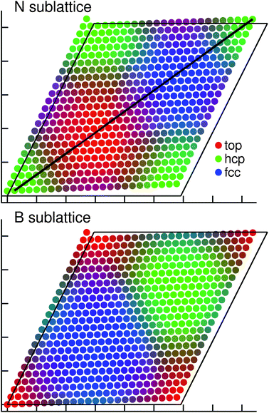 | ||
| Fig. 1 Registry of the N and B atoms in the corresponding sublattices relative to the metal substrate. The top, hcp and fcc registries are shown as the red, green and blue components of the point colors, respectively. Mixed colors indicate intermediate and bridging positions. The black line indicates the (11) diagonal of the monolayer surface from the top-right N atom, used for later evaluation (cf.Fig. 5). The frame shows the unit cell of the metal substrate for reference. Axis ticks at intervals of 10 Å. | ||
It is immediately evident that both B and N atoms occupy all three adsorption registries relative to Cu in approximately equal proportions. Additionally, there are boundary regions (3 to 4 BN units wide). They indicate atoms in bridging and intermediate sites. Note furthermore the differences between the two sublattices, which follow a cyclic pattern; regions with Btop contain Nhcp, Bhcp contain Nfcc, and Bfcc contain Ntop. The strongest variation of the adsorption registry occurs along the cell diagonal. Here, both atom species occupy all three registries and the corresponding transition zones. We indicate in the figure the diagonal starting at the top-right nitrogen atom, which we will refer back to in later sections.
3.2 Simulated STM images and electronic structure
STM experiments have revealed numerous interesting aspects of the h-BN–Cu system. In particular, it was observed that the surface shows a pattern of apparent height characterized by hills and valleys, which inverts at an applied bias voltage of 4.5 V. The fact that the topography varies strongly with the voltage indicates that the observed corrugation is predominantly electronic and not structural.16Fig. 2 shows a simulated STM image for the h-BN–Cu Moiré system at a bias of +1.0 V. The image shows a pattern of rounded hexagonal regions with a higher STM topography profile (brighter color) surrounded by darker, lower areas. The area directly above the elevated “hill” region contains more pronounced atom-like points with slightly greater height than the rest of the dark areas. The hill is surrounded by a fringe of lower elevation.
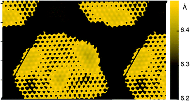 | ||
| Fig. 2 Simulated STM using Tersoff–Hamann approximation at a bias of +1.0 V. Color bar is in units of Å relative to the topmost Cu layer, the x and y axis ticks at intervals of 10 Å. Black lines indicate the unit cell. | ||
The central hill area corresponds approximately to the region with mostly NtopBfcc adsorption registry. The other two discernible areas are those with NfccBhcp (dark) and NhcpBtop (faint yellow points) registries. The overall variation of apparent height is approximately 0.3 Å, comparable to what is found experimentally for these bias voltages. As the topographic height is calculated from both the electron density and the electrostatic potential, the structural and electronic corrugations are convoluted. Therefore, the peak-to-peak height difference is larger in the simulated STM than in the optimized structure.
The electrostatic potential (ESP) above the surface can give further insight into the electronic structure of the studied system. Expressed relative to the Fermi energy, it reflects the local work function Φ. Fig. 3 shows a map of the ESP-derived work function across the surface of the supercell, cut at a height of about 3.4 Å above the h-BN layer. The potential varies in a range of 0.14 eV, showing an approximately circular minimum in the region of NtopBfcc configurations and a maximum further along the cell diagonal, around the NfccBhcp atoms. The other areas (of different registry) show roughly intermediate values for the ESP.
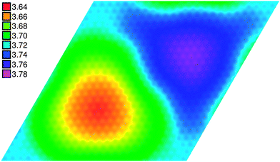 | ||
| Fig. 3 Lateral map of the electrostatic potential relative to the Fermi energy (eV) at constant height, approx. 3.4 Å above the h-BN layer. The area is the same as the unit cell drawn in Fig. 2. | ||
The three distinct regions of ESP are largely coincident with the three main areas of different contrast in the simulated STM images, although their shapes tend to be more rounded. The lateral variation in Φ we find is smaller than indicated by experiments (0.3 eV (ref. 16)), but qualitatively comparable as the hill is characterized by a lower work function than the valley. We find values of 3.64 eV and 3.78 eV for the minimum and maximum work functions, respectively. These values are also somewhat smaller than what is found experimentally (3.8 and 4.1 eV).
Fig. 4 shows plots of the projected densities of states (PDOS) on various atoms on the cell diagonal. We only indicate those states that are most strongly involved in the metal–substrate bonding, i.e. the pz states of B and N and the dz2 states of Cu. We focus on two regions of differing adsorption registry, Ntop and Nfcc and indicate for comparison the PDOS of these atoms in the isolated BN or metal. The lower panels in Fig. 4 show the PDOS from 1 × 1 calculations of NtopBfcc and NfccBhcp arrangements.
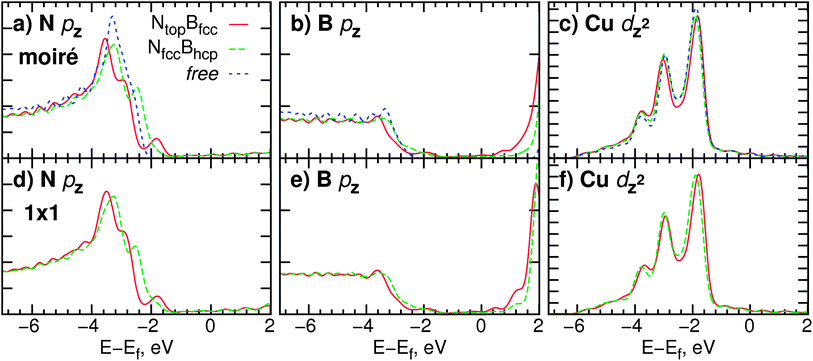 | ||
| Fig. 4 (a–c) Projected densities of states (PDOS) for N, B, and Cu (surface layer) atoms on the diagonal of the Moiré supercell (in the Ntop and Nfcc regions, cf.Fig. 1). The corresponding PDOS in a free-standing h-BN layer and bare Cu surface are plotted for comparison. (d–f) PDOS for corresponding atoms in 1 × 1 calculations of h-BN–Cu in NtopBfcc and NfccBhcp registries (bottom row). Vertical axis ticks indicate intervals of 0.05 states eV−1. | ||
The PDOS on nitrogen appears to be the one most affected by binding to the substrate. Compared to the pz states of the free layer, the main band at approx. −3 eV broadens upon adsorption and the magnitude of the PDOS is lowered, indicating some polarization away from N. An additional peak at about −1.9 eV appears in the PDOS of N in the fcc position, absent from both the free and the fcc curves. As this N atom is closest to the underlying Cu in the topmost layer, this peak presumably appears due to the increased interaction with the metal orbitals. Besides the emergence of this new feature, the pz bands are also shifted by approximately 0.2 eV. The fcc curve remains closer to the Fermi level, and is even somewhat up-shifted from the band of the free monolayer. Note, however, that the Ntop region of the cell has a lower work function. This can be rationalized with the shift of the main bands to lower energies. The down-shift of the Ntop band and the emergence of the additional small peak can also be seen in the corresponding 1 × 1 PDOS data. This would indicate that the local environment within the Moiré pattern is the major influence on the PDOS.
The PDOS for the B atoms in the same regions are shown in Fig. 4b. Here, amplitudes are lower by approximately a factor of 2 from the nitrogen case, and the curves are generally flat, with a gentle onset between −2 and −4 eV. The effect due to the adsorption is less visible, but we still observe a lowering and broadening of the PDOS curve. It should be noted that here B is found in Bfcc and Bhcp positions, being in both cases laterally distant from the topmost Cu, which presumably leads to weaker interactions. Close similarities with the 1 × 1 PDOS are also evident here, such as the relative shift of peaks and the position and width of the band gap.
The metal dz2 states (Fig. 4c) appear to be least affected by the adsorption of the monolayer. The bands largely retain their double-peak structure and do not shift. Only a small depletion may be observed in the Ntop case, hinting perhaps at the polarization from N to Cu noted above. By and large, the situation on the Moiré is comparable to the 1 × 1 case, with some small changes in the finer structure of the features.
It has been suggested7 that the Cu dz2 orbitals are largely unaffected by the h-BN–substrate interaction, which is instead dominated by pz–4s hybridization. Our data support this notion, showing on the one hand only marginal changes in the dz2 bands, and on the other hand a lowering and broadening of the 4s states in the range between −4 and −2 eV (see Fig. S1 in the ESI†). This is indeed evidence of some s–pz hybridization, which, although subtle, is the major contribution to the binding between the monolayer and substrate aside from the van der Waals interaction. Also these states, however, remain mostly unaffected by a change of the N registry, showing only very slight broadening in the Ntop configuration, compared to the Nfcc case.
Our results are in good agreement with electronic-structure data published by Laskowski and co-workers.13 Qualitatively, our data confirm the notion that the DOS of the metal surface remains mostly unchanged upon adsorption and that changes are subtle also in the adlayer. However, they only report adsorption in one registry, so that the effect of the relative placement of h-BN cannot be directly compared. Also quantitatively our results are similar to theirs, with Cu-dz2 band onsets just above −2 eV, a N-pz peak at roughly the same position, and the gentle B-pz onset between −4 and −2 eV.
Having presented the geometric and electronic properties of this Moiré system, we now relate the two in the next section.
3.3 Relationship between the geometric and electronic structure
As shown in the preceding sections, the electronic structure varies across the Moiré supercell, while the adsorbed monolayer is largely flat throughout. Our results are thus in contrast to previous studies of related adsorption systems, which have commonly rationalized a corrugation of the electronic structure with the pronounced concomitant corrugation of the monolayer.10,12,27 From a comparison of Fig. 2 and 3 with Fig. 1 it becomes evident that the patterns of the electronic structure resemble those produced by the lateral variation of the adsorption registry. It has already been suggested16 that the modulation of the registry is responsible for the observed electronic corrugation of the surface. In this context our calculations serve to provide an atomic-scale rationalization for this observation.The most pronounced variation of the adsorption registry occurs along the diagonal of the surface (vide supra), which we therefore examine in greater detail as a model for the entire supercell. In the top panel of Fig. 5 we plot the lateral distance of N atoms to their closest partners in the top, hcp and fcc layers along the diagonal (the black line in Fig. 1). For comparison, the vertical distance dCu to the metal surface is also plotted on the same vertical scale (shifted down by 2.5 Å). This plot illustrates the registry variation in greater detail than Fig. 1; the lower a point, the closer is a particular N atom to the ideal registry of that layer. We observe three minima, corresponding to almost “pure” Ntop, Nhcp, and Nfcc sites and three intersections of curves indicating interstitial positions. Over the same lateral distance, the topographic height remains largely unchanged, with a peak-to-peak difference of 0.12 Å. Fig. S2 in the ESI† shows the analogous plots for the registry of B along the same diagonal. The same picture emerges, with the exception of a phase shift, putting the Bfcc minimum at the position of the Ntop minimum, corresponding to the co-occurrence of these registries noted above.
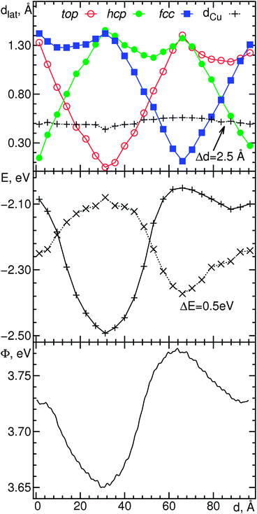 | ||
| Fig. 5 Relationship between the geometric and electronic structure in h-BN Moiré on Cu(111), along the cell diagonal indicated in Fig. 1. (a) Lateral distance (Å) of N atoms to the closest Cu atoms in the underlying top, hcp and fcc layers and vertical distance dCu to the surface (secondary vertical axis). Lines drawn to guide the eye. (b) Energy (eV) of the pz flank (continuous line) and peak (dashed line, secondary vertical axis) onsets of PDOS projected on N atoms along the cell diagonal. Lines drawn to guide the eye. (c) Approximate work function (eV) from electrostatic potential at 3.40 Å above the surface. Horizontal axis shows distance (Å) from the bottom left N atom in the cell. | ||
In the preceding discussion of the pz PDOS of nitrogen, we remarked the shift of the band onset and emergence of a small secondary peak for two registry extremes. Fig. 5b shows the position (in eV) of the flank of the band onset and the position of the peak in the PDOS projected on each atom along the diagonal. For this purpose, we have arbitrarily defined the onset of the flank (Efl) as the point where the value of the PDOS is equal to 0.040 states per eV, and the onset of the peak (Ep) as the point with a value of 0.020 states per eV. Efl varies in a range greater than 0.4 eV, with one pronounced minimum, while Ep follows an inverted trend with a somewhat smaller range of onset energies. By comparing this plot with the variation of the surface registry, it is obvious that Efl closely tracks the curve of the top registry, and Ep follows it with the opposite sign. Thus, at the point where the N atoms are closest to an underlying Cu, their pz flanks are most strongly shifted to lower energies, while the smaller feature is closest to the Fermi level. In the opposite extreme of a large lateral N–Cu separation, the two features are closest together and the peak disappears into the flank (note the shift of curves in Fig. 5b).
Evidently, the distance between a N atom and its closest Cu strongly influences the local electronic structure of that atom. In the present system, however, it is the lateral rather than the vertical distance which is responsible for the shift of the PDOS features, as it is much more strongly modulated along the cell diagonal. Additionally, when the metal slab is removed, the variation of the electrostatic potential is reduced by a factor of 3.5, confirming that the monolayer corrugation plays a minor role in modulating the electronic structure.
Fig. 5c shows a cut through the electrostatic potential (cf.Fig. 3) on the cell diagonal, 3.4 Å above the surface. While the variation is smaller than that based on the PDOS features, it also follows the same characteristic variation related to the Ntop registry. Thus, the work function reaches a minimum at Ntop and a maximum at Nfcc positions. We relate this to the trend of Efl, indicating that the conduction band is down-shifted furthest exactly at positions of smallest Φ, and vice versa. The absolute value of the work function should decrease as cuts of the electrostatic potential are considered further away from the surface. This is also the reason why the peak-to-peak difference of the ESP gets progressively smaller at larger distances, as the local features of the electronic structure are increasingly smeared out. A difference of 0.14 eV at 3.4 Å is reduced to 0.092 eV at 4.8 Å and 0.073 eV at 6.3 Å.
Based on these data, it becomes evident that the adsorption registry connects the electronic structure with the underlying geometry. The lattice mismatch and rotation of the monolayer cause a modulation of the adsorption registry over the cell. This in turn results in a periodic variation of the (lateral) B,N–Cu distances, changing the hybridization between metal and BN. Consequently, features of the PDOS change depending on the position of each atom, resulting finally in a modulated electrostatic potential at considerable distance above the surface. Therefore, the experimentally observed electrostatic corrugation can originate without significant structural changes.
4 Conclusions
Our results support the previously reported notion that the interaction between h-BN and Cu is rather weak7,13 and causes only minute structural changes in both the adsorbate and substrate. Over short length scales, the small mismatch between the two lattices facilitates the formation of quasi-commensurate 1 × 1 structures. Depending on the relative placement of the layers, these can differ with regard to energetic and electronic properties, but variations are generally small. We attribute this to the weak electronic interaction between the substrate and monolayer, resulting in a predominantly physisorption-like binding governed by van der Waals interactions. This inertness of Cu to h-BN can be favorable for applications where it is desirable to decouple an adsorbate from the metal surface or when the monolayer is to be detached from the substrate after formation.However, experimental evidence16 combined with theoretical knowledge about the formation of Moiré patterns on surfaces8 suggests that there is more to the story of h-BN on Cu(111). Our results confirm and substantiate the observations of electrostatic corrugation in h-BN–Cu without concomitant structural deformations. Such patterns could be utilized to preferentially adsorb molecules on particular areas of the surface and thus assemble well-defined two-dimensional arrangements. As the h-BN layer in the present system remains flat, adsorption of large two-dimensional molecules should be facilitated since there are no pores that impose steric constraints on the adsorbate. One could envision tuning the periodicity of the electrostatic corrugation by modifying the rotation angle and lattice mismatch in order to obtain fine control over adsorbate placement.
In summary, our study has led to a deeper understanding of a large h-BN–Cu Moiré system at the atomic-scale. As we analyze the electronic structure of the surface (using simulated STM images, projected densities of states, and the electrostatic potential) it becomes apparent that these features are correlated with the distance between B or N and the topmost metal atoms. We show that, as the monolayer remains structurally uncorrugated, the lateral modulation of the adsorption registry is the main factor responsible for the change in interatomic distances, thus affecting hybridization and with it aspects of the electronic structure.
Acknowledgements
We thank Willi Auwärter, Johannes V. Barth, and co-workers for fruitful discussions and valuable input from the experimental perspective. We gratefully acknowledge financial support from the Swiss National Science Foundation under grant no. 20021-140441 and generous computing resources from the Swiss National Supercomputing Center (project ID: S89).References
- T. Greber and C. Oshima, J. Phys.: Condens. Matter, 2012, 24, 310201 CrossRef.
- F. Schwierz, Nat. Nanotechnol., 2010, 5, 487–496 CrossRef CAS.
- J. D. Fowler, M. J. Allen, V. C. Tung, Y. Yang, R. B. Kaner and B. H. Weiller, ACS Nano, 2009, 3, 301–306 CrossRef CAS.
- H. Ma, T. Brugger, S. Berner, Y. Ding, M. Iannuzzi, J. Hutter, J. Osterwalder and T. Greber, ChemPhysChem, 2010, 11, 399–403 CrossRef CAS.
- B. Wang and M.-l. Bocquet, J. Phys. Chem. Lett., 2011, 2, 2341–2345 CrossRef CAS.
- M. Corso, W. Auwärter, M. Muntwiler, A. Tamai, T. Greber and J. Osterwalder, Science, 2004, 303, 217–220 CrossRef CAS.
- A. B. Preobrajenski, A. S. Vinogradov and N. Martensson, Surf. Sci., 2005, 582, 21–30 CrossRef CAS.
- K. Hermann, J. Phys.: Condens. Matter, 2012, 24, 314210 CrossRef.
- D. Martoccia, P. Willmott, T. Brugger, M. Björck, S. Günther, C. Schlepütz, A. Cervellino, S. Pauli, B. Patterson, S. Marchini, J. Wintterlin, W. Moritz and T. Greber, Phys. Rev. Lett., 2008, 101, 1–4 CrossRef.
- B. Wang, M.-L. Bocquet, S. Marchini, S. Günther and J. Wintterlin, Phys. Chem. Chem. Phys., 2008, 10, 3530–3534 RSC.
- D. Stradi, S. Barja, C. Díaz, M. Garnica, B. Borca, J. Hinarejos, D. Sánchez-Portal, M. Alcamí, A. Arnau, A. Vázquez de Parga, R. Miranda and F. Martín, Phys. Rev. Lett., 2011, 106, 186102 CrossRef CAS.
- M. Iannuzzi and J. Hutter, Surf. Sci., 2011, 605, 1360–1368 CrossRef CAS.
- R. Laskowski, P. Blaha and K. Schwarz, Phys. Rev. B, 2008, 78, 045409 CrossRef.
- K. K. Kim, A. Hsu, X. Jia, S. M. Kim, Y. Shi, M. Hofmann, D. Nezich, J. F. Rodriguez-Nieva, M. Dresselhaus, T. Palacios and J. Kong, Nano Lett., 2012, 12, 161–166 CrossRef.
- L. Song, L. Ci, H. Lu, P. B. Sorokin, C. Jin, J. Ni, A. G. Kvashnin, D. G. Kvashnin, J. Lou, B. I. Yakobson and P. M. Ajayan, Nano Lett., 2010, 10, 3209–3215 CrossRef CAS.
- S. Joshi, D. Ecija, R. Koitz, M. Iannuzzi, A. P. Seitsonen, J. Hutter, H. Sachdev, S. Vijayaraghavan, F. Bischoff, K. Seuferd, J. V. Barth and W. Auwärter, Nano Lett., 2012, 12, 5821–5828 CrossRef CAS.
- J. Gomez-Diaz, Y. Ding, R. Koitz, A. P. Seitsonen, M. Iannuzzi and J. Hutter, Theor. Chem. Acc., 2013, 132, 1–17 CrossRef CAS.
- J. VandeVondele, M. Krack, F. Mohamed, M. Parrinello, T. Chassaing and J. Hutter, Comput. Phys. Commun., 2005, 167, 103–128 CrossRef CAS.
- CP2K developers group under the terms of the GNU General Public Licence; see http://www.cp2k.org, 2012.
- J. VandeVondele and J. Hutter, J. Chem. Phys., 2007, 127, 114105 CrossRef.
- S. Goedecker, M. Teter and J. Hutter, Phys. Rev. B, 1996, 54, 1703–1710 CrossRef CAS.
- Y. Zhang and W. Yang, Phys. Rev. Lett., 1998, 80, 890–891 CrossRef CAS.
- S. Grimme, J. Antony, S. Ehrlich and H. Krieg, J. Chem. Phys., 2010, 132, 154104 CrossRef.
- J. Tersoff and D. R. Hamann, Phys. Rev. Lett., 1983, 50, 1998–2001 CrossRef CAS.
- D. R. Hamann, Phys. Rev. B, 1985, 31, 805–813 CrossRef.
- G. Grad, P. Blaha, K. Schwarz, W. Auwärter and T. Greber, Phys. Rev. B, 2003, 68, 1–7 CrossRef.
- T. Brugger, H. Ma, M. Iannuzzi, S. Berner, A. Winkler, J. Hutter, J. Osterwalder and T. Greber, Angew. Chem., Int. Ed., 2010, 49, 6120–6124 CrossRef CAS.
Footnote |
| † Electronic supplementary information (ESI) available. See DOI: 10.1039/c3nr00709j |
| This journal is © The Royal Society of Chemistry 2013 |