 Open Access Article
 This Open Access Article is licensed under a Creative Commons Attribution-Non Commercial 3.0 Unported Licence
Ultrasonic-assisted self-assembly of monolayer graphene oxide for rapid detection of Escherichia coli bacteria
Jingbo Changa, Shun Maoa, Yang Zhanga, Shumao Cuia, Guihua Zhoua, Xiaogang Wub, Ching-Hong Yangb and Junhong Chen*a
aDepartment of Mechanical Engineering, University of Wisconsin-Milwaukee, 3200 North Cramer Street, Milwaukee, WI 53211, USA. E-mail: jhchen@uwm.edu
bDepartment of Biological Science, University of Wisconsin-Milwaukee, 3200 North Cramer Street, Milwaukee, WI 53211, USA
First published on 6th March 2013
Abstract
Due to potential risks to the environment and human health arising from pathogens/chemical contaminants, novel devices are being developed for rapid and precise detection of those contaminants. Here, we demonstrate highly sensitive and selective field-effect transistor (FET) sensor devices for detection of Escherichia coli (E. coli) bacteria using thermally reduced monolayer graphene oxide (TRMGO) sheets as semiconducting channels. The graphene oxide (GO) sheets are assembled on the aminoethanethiol (AET)-functionalized gold (Au) electrodes through electrostatic interactions with ultrasonic assistance. Anti-Escherichia coli (anti-E. coli) antibodies are used as receptors for selective detection of E. coli cells and integrated on the FET device through covalent bonding with Au nanoparticles on the GO surface. The TRMGO FET device shows great electronic stability and high sensitivity to E. coli cells with a concentration as low as 10 colony-forming units (cfu) per mL. The biosensing platform reported here is promising for large-scale, sensitive, selective, low-cost, and real-time detection of E. coli bacteria.
1 Introduction
Escherichia coli (E. coli) bacteria are among the most prevalent infectious organisms that exist widely in the environment and can spread quickly and easily through water and food at an appropriate temperature.1–4 The worst type of E. coli, known as E. coli O157:H7, is a major food-borne and water-borne pathogen that causes bloody diarrhea, hemorrhagic colitis, and hemolytic uremic syndrome.5–7 In serious conditions, E. coli O157:H7 can sometimes cause kidney failure and may lead to death. Real-time monitoring of this pathogen in food production and in water is critical to prevent its spread, and many methods have been developed to detect E. coli O157:H7, such as the culture and colony counting method,8 polymerase chain reaction (PCR),9–12 and the immunological method.13,14 These methods have limitations with respect to low sensitivity and less specificity, and are time-consuming.Stimuli-responsive field-effect transistors (FETs) are very attractive for sensing applications due to their rapid response, high sensitivity, and real-time monitoring.15 Because of small sensor-to-sensor variations and high reproducibility, integrating a material as an active channel into an FET device is a practical approach for sensing applications. Due to the high sensitivity of devices to the gating effect, carbon nanomaterials show great promise for applications as transducer components of various chemical and biological sensors. Graphene, a single layer of carbon atoms packed into a two-dimensional honeycomb lattice, is a promising semiconducting channel material for FETs due to its unique electrical, physical, and optical properties.16–19 Intrinsic graphene is a zero-gap semiconductor that has remarkably high electron mobility (100 times greater than that of silicon), making it ideally suitable for electronic devices, energy storage, and atomic-scale, high-speed chemical/biological sensors.20 Graphene can be prepared at a low cost by reducing graphene oxide (GO). In particular, thermally reduced graphene oxide (TRGO)-based biological sensing systems have been developed with advantages such as tunable electronic properties (ambipolar, n- or p-type semiconducting behavior), simple device structure, and label-free detection.21,22 Fabrication of TRGO devices has been demonstrated using the drop-casting method or the spin-coating method;23,24 alternatively, dielectrophoresis has been used to trap GO sheets at predefined locations (e.g., electrodes).25 By using simple solution processes to prepare GO films, the single-layer GO sheets tend to fold and wrinkle at edges to resist collapsing into multilayers or randomly overlaying monolayers during the evaporation of solvents.26 In our previous report, we have successfully fabricated a highly sensitive and selective thermally reduced GO FET biosensor platform using the drop-casting method;27 however, the sensing performance of the resulting GO FETs can be significantly affected by the number of GO sheets in the device, e.g., GO sheet–sheet screening effects.28
Here we report the self-assembly of monolayer GO nanosheets on the photolithographically patterned gold (Au) electrodes for highly sensitive detection of E. coli O157:H7. Our strategy uses the electrostatic interaction between the reactive oxygen-containing functional groups (oxygen epoxide groups, carboxyl, and carbonyl groups decorated on the sheet edges) of fully exfoliated individual GO sheets and amino group (NH2)-functionalized electrodes, to selectively immobilize GO sheets on the electrode. This fabrication method by a solution process is suitable for mass-production of GO FET sensors. Due to the strong electrostatic adsorption between the NH2-modified electrodes and the first layer of the deposited GO sheet,29 excessive GO sheets from the multilayer can be easily removed by rinsing and sonication in deionized water. The deposited monolayer GO sheets are subsequently reduced by the thermal annealing process to convert the insulating GO into semiconducting thermally reduced monolayer graphene oxide (TRMGO). The obtained TRMGO-FET devices can be configured into electrical biosensors based on the top gating structure. Because the target biomolecules are charged, sensor sensing signals can be monitored directly by the change in FET electrical properties (e.g., current or conductance). Our results show that TRMGO-based FET immunosensors have high sensitivity for detecting E. coli cells with short response time and high reproducibility.
2 Materials and methods
2.1 Materials
GO was ordered from ACS MATERIAL, which was synthesized by using the modified Hummer's method. First, 2-aminoethanethiol (AET) and glutaraldehyde (GA) were purchased from Sigma-Aldrich. Tween 20 and cold water fish gelatin were ordered from Tedpella. Anti-E. coli O157:H7 antibodies and E. coli O157:H7 cells were purchased from KPL, Inc. PBS (pH 7.4, ×1) (Fisher BioReagents) was used as the solvent for anti-E. coli O157:H7 antibodies. All solutions were prepared with deionized (DI) water (Cellgro). Cell culture grade water was purchased from Mediatech, Inc.2.2 Device fabrication
TRMGO FETs were fabricated by self-assembly of GO sheets on the AET-modified Au interdigitated electrodes with both finger-width and inter-finger spacing (source and drain separation) of about 2 μm and a thickness of 50 nm. The electrodes were fabricated using a photolithography process on a highly doped Si wafer with a top layer of dry-formed SiO2 (thickness of 200 nm). The prepared electrodes were immersed in AET (1 mg mL−1) solution at a concentration of 10 mM for 10 min and a monolayer of AET was assembled on the electrodes. The modified device was immersed in a GO dispersion with the assistance of sonication (Bransonic 1510-DTH); without sonication, the multilayer or folded layers of GO will form on the electrodes. After 1 min, a monolayer of the GO film was deposited on the electrodes due to electrostatic interactions. The device was next annealed in an argon flow (1 liter per minute) for 1 h at 400 °C to reduce oxygen-containing groups in order to improve the semiconducting property and to reduce the junction barriers between the Au electrodes and TRMGO. Isolated Au nanoparticles (NPs) as scaffolds for immobilizing special probes were deposited on the TRMGO using an RF (60 Hz) Emitech K550x sputter coater apparatus with an Au target (99.999% purity) at an Ar pressure of 0.03 mbar. The deposition time was 2 s with a working current of 10 mA.2.3 Immobilization
The prepared device was immersed in an AET (1 mg mL−1) solution with a concentration of 10 mM for 1 h. After being thoroughly rinsed with DI water and dried under a stream of nitrogen gas, the modified device was treated with a 25% GA solution at 25 °C for 1 h. After that, the device was incubated in the PBS containing anti-E. coli O157 (10 μg mL−1) antibodies at 4 °C for 12 h. Finally, the device was incubated with a blocking buffer (0.1% Tween 20) for 2 h at room temperature and then washed with the cell culture water.2.4 Characterization
Electrical measurements were performed on TRMGO sensors using a Keithley 4200 semiconductor characterization system at room temperature. The sensing signal of the device was recorded by monitoring the change in the drain current (ISD) for a given source–drain voltage (VSD) when the device was exposed to different concentrations of target materials.3 Results and discussion
To control the device-to-device variation and electronic stability of devices, it is crucial to form a uniform GO film on the device. Our strategy is to employ an electrostatic self-assembly method to deposit GO sheets on the amino-terminated Au electrodes.30Fig. 1a illustrates the chemical anchoring procedure for modifying Au electrodes with AET (see Experimental section), leading to the formation of a thin AET film. AET was assembled on the Au surface because of the strong affinity of sulfur in the thiol functional groups.31 The monolayer of AET packs tightly due to van der Waals interactions, thereby reducing its own free energy. The amino groups of AET can interact with the functional groups (e.g., carboxylic acid) on the GO surface, leading to self-assembly of the GO sheets on the electrodes as shown in Fig. 1b. The first GO layer is strongly adhered to the electrodes by electrostatic adsorption, but the excessive GO sheets from multilayers can be removed under well-controlled sonication.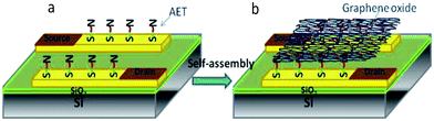 | ||
| Fig. 1 Schematic illustration of (a) a layer of AET coating on the electrode surface and (b) self-assembly of GO sheets on the AET-modified electrodes. | ||
To investigate the topographies of self-assembled TRMGO sheets on the electrodes, scanning electron microscopy (SEM) and atomic force microscopy (AFM) were employed. Fig. 2a shows SEM images of TRMGO distribution on Au electrodes. The lateral dimensions of TRMGO sheets typically ranged from several hundred nanometers to several micrometers on the devices with largest TRMGO sheets exceeding 3 μm (Fig. 2a). The area density of TRMGO sheets across electrodes was evaluated as approximately 5 sheets per 10 μm2, which confirms that TRMGO sheets were uniformly distributed on the modified electrodes.
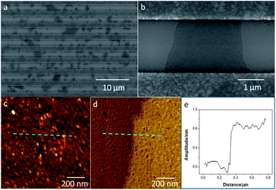 | ||
| Fig. 2 (a and b) SEM images of TRMGO sheets across the electrode gaps. AFM data (tapping mode) of TRMGO on the silicon wafer: (c) height and (d) phase images of the same zone at a cross-sectional area. The dashed line indicates a scanning trace of the TRMGO. (e) Height profile of TRMGO obtained by scanning from bare silicon wafer to TRMGO. | ||
Fig. 2b shows an individual transparent TRMGO sheet on the electrodes, which indicates that the GO sheet is comfortably positioned across the gap between the electrodes. Fig. 2c and d show AFM images of a TRMGO sheet on the device. The thickness of the sheet measured through the cross-sectional height profiles from AFM data is 0.8–0.9 nm, which is consistent with monolayer TRMGO sheets.32 Recent studies have shown that GO sheets in aqueous solution readily form crumpled graphene on substrates under the action of water surface tension during aerosol microdroplet drying.26,33 In this study, both SEM and AFM images show that GO monolayers are morphologically stable with respect to the thermal reduction process. The self-assembly mechanism with the assistance of sonication is electrostatic attraction through surface chemical modification, which can prevent the GO sheet from crumpling on the devices.
For FET sensors, the field effect responses of TRMGO devices should be rapid and sensitive. To investigate the electrical properties of TRMGO FET devices, measurements were carried out in air at room temperature using the back-gated FET devices. Fig. 3a shows the typical ISD–VG characteristics of a TRMGO FET device, in which VG is the gate voltage and ISD is the drain current. While the gate bias was varied from −40 to +40 V, the current of the device decreased from 139 to 59 nA. The decrease in conductivity with increasing voltage indicates that the TRMGO sheets are p-type semiconducting materials. More importantly, the proposed TRMGO device shows good switching performance with an on/off current ratio of 2.35. We have repeated more than one hundred devices, which show similar electrical properties such as conductivity (∼140 kΩ) and current on/off ratio (∼2.3). This result implies that our electrostatic self-assembly method with the assistance of ultrasonication can be used to form stable, uniform devices over a large area without aggregation.
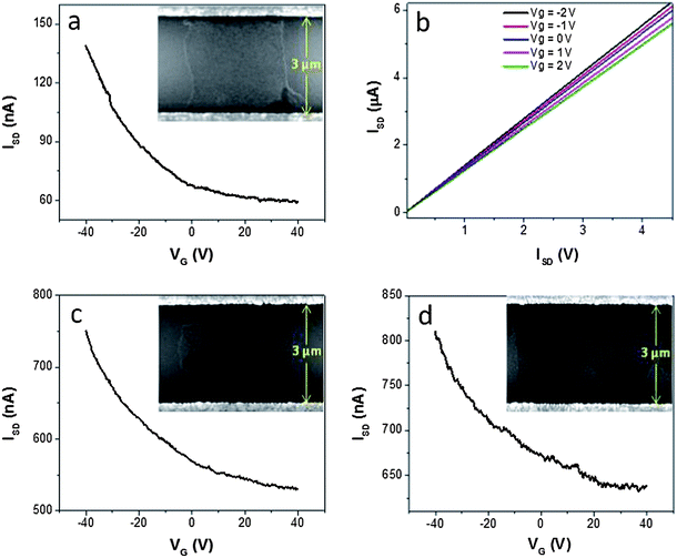 | ||
| Fig. 3 (a) The FET I–V curve of TRMGO on a SiO2/Si substrate (ISD = 100 mV). The inset shows an SEM image of a monolayer GO sheet bridging the electrode gap. (b) ISD–VSD output characteristics of the TRMGO FET device at different bottom-gate VG from −2 to 2 V with an interval of 1 V. (c) The FET I–V curve of the crumpled GO FET device. The inset shows an SEM image of a crumpled GO across the electrode gap. (d) The FET I–V curve of the multilayer GO FET device. The inset shows an SEM image of multilayer GO sheets across the electrode gap. | ||
To further examine the electrical characteristics of TRMGO FET devices, a bottom-gate voltage was applied on the devices from −2 to 2 V with an interval of 1 V. The drain–source current decreased with increasing gate voltage, as shown in Fig. 3b, which indicates that the device response is sensitive to the gate voltage. Moreover, devices displayed an Ohmic-contact behavior, indicating that the sensing mechanism in the TRMGO FET system is dominated by electrostatic gating. In the sonication–fabrication process of the device, GO sheets deposited on the electrodes by the self-assembly method are monolayer and transparent, and the GO-based FET device shows good semiconducting properties. Without sonication, GO sheets deposited on the electrodes are likely to form folded or multilayer GO films (insets of Fig. 3c and d), leading to devices with a lower on/off current ratio (1.41 and 1.27 for folded and multilayer GO, respectively). For FET biosensor applications, it is generally believed that the sensitivity has a strong dependence on the on/off current ratio of sensors,34 especially on the subthreshold slope.35 To achieve higher-performing FET biosensors, TRMGO devices are promising candidates compared with multilayer or folded GO devices according to the FET sensor mechanism.
The sensing performance of TRMGO FET devices was investigated using anti-E. coli antibodies as probes. The device was exposed to various concentrations of E. coli cells in the cell culture grade water. The changes in transfer curves of the FET sensor after adding selected concentrations of E. coli cells (10, 102, 103, and 104 cfu mL−1) have been investigated. It can be observed that the conductance of the devices continued to increase with increasing concentrations of E. coli cells (Fig. 4a). As the TRMGO FET was operated in the p-type region (VG = 0 V), the device conductance increase is due to increased hole concentration, which is induced by the highly negatively charged bacterial wall and is in agreement with previous reports.28,36
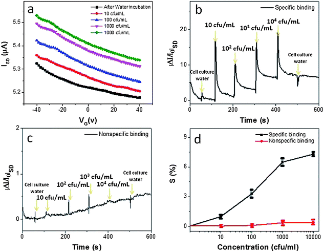 | ||
| Fig. 4 (a) Typical gate voltage dependence (VSD = 0.1 V) of ISD upon the introduction of E. coli cells of different concentrations. (b) Dynamic response of the devices exposed to different concentrations of E. coli cells for specific binding in the TRMGO FET device. (c) Non-specific binding in the TRMGO FET device (without anti-E. coli antibody probes). (d) The calibration curve of the TRMGO FET device (sensitivity S = ΔI/I0vs. concentration). Error bars were obtained through multiple measurements. | ||
The dynamic response of TRMGO-based devices for detecting E. coli cells was measured with the specific binding as shown in Fig. 4b and non-specific binding as shown in Fig. 4c, respectively. The conductance of the device with specific binding increased correspondingly with the addition of E. coli cell solution, and the current change of the device was around 1.1% with the introduction of 10 cfu mL−1. For comparison, a control experiment was carried out on a device without modification of anti-E. coli antibody probes. In contrast, controlled injection of E. coli cells had almost no effect on the conductance of the TRMGO devices in the absence of probes (Fig. 4c). Therefore, it is confirmed that the conductance increase is solely attributed to the specific binding between probes and target materials.
The sensor sensitivity (relative conductivity change, %) is presented as a function of E. coli cell concentration in Fig. 4d. The TRMGO device had a higher sensitivity for all E. coli cell concentrations than that of the device with non-specific binding. For specific binding, the sensitivity gradually increased linearly for E. coli cell concentrations from 10 cfu mL−1 to 103 cfu mL−1 and the response amplitude depends on the E. coli cell concentration. If more E. coli cells bind to anti-E. coli antibodies on the devices, a larger gating effect will be introduced and more significant carrier concentration change will result,37 thereby leading to more conductivity change in the sensor. This sensing mechanism was also confirmed by transfer curves in a previous report;36 however, at a higher concentration of 104 cfu mL−1, the sensor signal was not directly proportional to the increased cell concentration because the sensor became saturated. This phenomenon indicates that most of the binding sites on the devices are occupied by target analytes at the 104 cfu mL−1 concentration level. For non-specific binding (without anti-E. coli cell probes), the TRMGO device showed only a very weak response, because the blocking buffer can effectively block physical adsorption of E. coli cells on the device. The concentration-dependent responses of TRMGO devices can be analyzed using the Langmuir isotherm model according to a previous report.38 Thus, the normalized sensitivity N can be written as
| N = c(1/k + c)−1 |
To establish the sensor's specificity for E. coli cells, the sensor was interrogated with the non-pathogenic E. coli strain DH5a (104 cfu mL−1) and the plant-pathogenic bacterium Dickeya dadantii 3937 (104 cfu mL−1) with the same procedure as that used for specific detection of the E. coli O157:H7 cells. The performance evaluation of the sensor's specificity is summarized in Fig. 5. It indicates that the sensor sensitivity from the E. coli DH5α (1.4%) and Dickeya dadantii 3937 (1.3%) is significantly smaller than that from the E. coli O157:H7 (7.3%). This result further confirms that the sensor response is from the binding of E. coli cells to anti-E. coli antibodies and the target materials can be selectively detected by the TRMGO FET sensor.
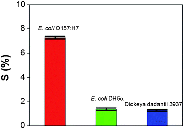 | ||
| Fig. 5 Comparison of the sensor sensitivity in response to E. coli O157:H7 (104 cfu mL−1), E. coli DH5α (104 cfu mL−1), and Dickeya dadantii 3937 (104 cfu mL−1). Error bars were obtained through multiple sample measurements. | ||
Recently, several research groups also attempted to enhance sensor sensitivity for detecting E. coli cells. Huang et al. reported that they developed a nanoelectronic biosensor for detecting E. coli bacteria with high sensitivity (10 cfu mL−1) using chemical-vapor-deposition-grown large-sized graphene as the active FET channel material.37 Wang et al. presented surface plasmon resonance biosensors based on the spectroscopy of grating-coupled long-range surface plasmons combined with magnetic nanoparticle assay for rapid and highly sensitive detection of bacterial E. coli cells with a detection limit of 50 cfu mL−1.39 Our sensor platforms have shown a comparable detection limit (10 cfu mL−1). Furthermore, in the device fabrication process, the number of GO layers on the electrodes can be controlled by the self-assembly method with sonication, which will lead to high reproducibility in the device fabrication and highly stable electrical properties of devices.
Understanding the sensing mechanism for E. coli cell detection can lead to better designs of TRMGO sensor devices and more reliable sensor fabrication procedures. In the case of FET biosensor devices, proposed mechanisms include charge-induced electrostatic gating and the Schottky barrier effect. Due to the high temperature (400 °C) during the annealing process, the Schottky barrier effect can be neglected, as reflected in Fig. 3b. From the above discussion of sensor response from specific and non-specific bindings, it is believed that the gate modulation (FET performance) leads to the sensor signal by capturing negatively charged E. coli cells. And the device conductivity change is attributed to the direct electrostatic gating effect from the accumulation of negatively charged E. coli cells on the gate electrode. Ishikawa et al. reported on the dependence of FET biosensor performance on the carbon nanotube density due to percolation and tube–tube screening effects, and demonstrated that the control of the nanotube density is critical to achieve high/reliable performance (e.g., high sensitivity, uniformity, and reproducibility).30 In our experiments, it is easy to control the quality of GO deposition on the devices, such as coverage fraction by adjusting the assembly time, monolayer deposition by varying the sonicator power, and selected-area deposition by electrode surface design and modification. The monolayer TRMGO devices can effectively avoid the layer–layer charge screening effect and maximize the performance of TRGO-based sensors.
4 Conclusion
We have demonstrated ultra-sensitive detection of E. coli cells using TRMGO FET devices. Fabricating the TRMGO devices can be easily scaled up with good reproducibility and high electrical stability. Monolayer GO sheets were selectively deposited on the electrodes by the self-assembly method with a density of 5 sheets per 10 μm2. Using a thermal annealing step, the GO can be reduced and the contact between GO and electrodes could be improved to anchor GO sheets on the electrodes. The TRMGO sensor platform with immobilized anti-E. coli antibodies demonstrated real-time, label-free, step-wise, target-specific, and highly sensitive electrical detection of E. coli cells at concentrations as low as 10 cfu mL−1, and the sensitivity increases with increasing E. coli concentrations up to 103 cfu mL−1. Our sensor platform offers a promising route for large-scale, high-performance chemical sensor and biosensor applications.Acknowledgements
Financial support for this work was provided by the U.S. National Science Foundation through Industry/University Cooperative Research Center on Water Equipment & Policy located at the University of Wisconsin-Milwaukee and Marquette University (IIP-0968887) and a fundamental research grant (IIP-1128158), and the University of Wisconsin-Milwaukee Research Foundation Bradley Catalyst Grant. The e-beam lithography was performed at the Center for Nanoscale Materials of Argonne National Laboratory, which is supported by the U.S. Department of Energy, Office of Science, Office of Basic Energy Sciences, under Contract no. DE-AC02-06CH11357. The authors thank Dr H. A. Owen for technical support with SEM analyses and Dr S. E. Hardcastle for help with AFM analyses.Notes and references
- M. S. Cheng, S. H. Lau, V. T. Chow and C. S. Toh, Environ. Sci. Technol., 2011, 45, 6453–6459 CrossRef CAS.
- A. K. Singh, D. Senapati, S. G. Wang, J. Griffin, A. Neely, P. Candice, K. M. Naylor, B. Varisli, J. R. Kalluri and P. C. Ray, ACS Nano, 2009, 3, 1906–1912 CrossRef CAS.
- K. Sen, J. L. Sinclair, L. Boczek and E. W. Rice, Environ. Sci. Technol., 2011, 45, 2250–2256 CrossRef CAS.
- E. Majid, K. B. Male and J. H. T. Luong, J. Agric. Food Chem., 2008, 56, 7691–7695 CrossRef CAS.
- S. D. Richardson, Anal. Chem., 2012, 84, 747–778 CrossRef CAS.
- S. D. Richardson and T. A. Ternes, Anal. Chem., 2011, 83, 4614–4648 CrossRef CAS.
- Z. B. Bahsi, A. Buyukaksoy, S. M. Olmezcan, F. Simsek, M. H. Aslan and A. Y. Oral, Sensors, 2009, 9, 4890–4900 CrossRef CAS.
- K. S. Gracias and J. L. McKillip, Can. J. Microbiol., 2004, 50, 883–890 CrossRef CAS.
- P. M. Fratamico and C. DebRoy, Food Anal. Methods, 2010, 3, 330–337 CrossRef.
- J. Singh, V. K. Batish and S. Grover, Foodborne Pathog. Dis., 2009, 6, 1195–1201 CrossRef CAS.
- S. Kawasaki, P. M. Fratamico, N. Horikoshi, Y. Okada, K. Takeshita, T. Sameshima and S. Kawamoto, Foodborne Pathog. Dis., 2009, 6, 81–89 CrossRef CAS.
- J. Singh, V. K. Batish and S. Grover, Foodborne Pathog. Dis., 2009, 6, 395–400 CrossRef CAS.
- L. X. Wang, C. S. Wu, X. D. Fan and A. Mustapha, Int. J. Food Microbiol., 2012, 156, 83–87 CrossRef CAS.
- Z. Y. Li, L. He, N. Y. He, Z. Y. Shi, H. Wang, S. Li, H. N. Liu and Y. B. Dai, Acta Chim. Sin., 2010, 68, 251–256 CAS.
- T. Q. Trung, N. T. Tien, D. Kim, J. H. Jung, O. J. Yoon and N. E. Lee, Adv. Mater., 2012, 24, 5254–5260 CrossRef CAS.
- A. H. Loo, A. Bonanni and M. Pumera, Nanoscale, 2012, 4, 143–147 RSC.
- F. N. Xia, D. B. Farmer, Y. M. Lin and P. Avouris, Nano Lett., 2010, 10, 715–718 CrossRef CAS.
- L. Vicarelli, M. S. Vitiello, D. Coquillat, A. Lombardo, A. C. Ferrari, W. Knap, M. Polini, V. Pellegrini and A. Tredicucci, Nat. Mater., 2012, 11, 865–871 CrossRef CAS.
- F. N. Xia, T. Mueller, Y. M. Lin, A. Valdes-Garcia and P. Avouris, Nat. Nanotechnol., 2009, 4, 839–843 CrossRef CAS.
- P. Avouris, Nano Lett., 2010, 10, 4285–4294 CrossRef CAS.
- W. W. Li, X. M. Geng, Y. F. Guo, J. Z. Rong, Y. P. Gong, L. Q. Wu, X. M. Zhang, P. Li, J. B. Xu, G. S. Cheng, M. T. Sun and L. W. Liu, ACS Nano, 2011, 5, 6955–6961 CrossRef CAS.
- O. S. Kwon, S. J. Park, J. Y. Hong, A. R. Han, J. S. Lee, J. S. Lee, J. H. Oh and J. Jang, ACS Nano, 2012, 6, 1486–1493 CrossRef CAS.
- S. Y. Bae, I. Y. Jeon, J. Yang, N. Park, H. S. Shin, S. Park, R. S. Ruoff, L. M. Dai and J. B. Baek, ACS Nano, 2011, 5, 4974–4980 CrossRef CAS.
- O. C. Compton and S. T. Nguyen, Small, 2010, 6, 711–723 CrossRef CAS.
- B. R. Burg, F. Lutolf, J. Schneider, N. C. Schirmer, T. Schwamb and D. Poulikakos, Appl. Phys. Lett., 2009, 94, 053110 CrossRef.
- X. F. Ma, M. R. Zachariah and C. D. Zangmeister, Nano Lett., 2012, 12, 486–489 CrossRef CAS.
- S. Mao, G. H. Lu, K. H. Yu, Z. Bo and J. H. Chen, Adv. Mater., 2010, 22, 3521–3526 CrossRef CAS.
- N. J. Lee, J. W. Yoo, Y. J. Choi, C. J. Kang, D. Y. Jeon, D. C. Kim, S. Seo and H. J. Chung, Appl. Phys. Lett., 2009, 95, 222107 CrossRef.
- T. Kurkina, S. Sundaram, R. S. Sundaram, F. Re, M. Masserini, K. Kern and K. Balasubramanian, ACS Nano, 2012, 6, 5514–5520 CrossRef CAS.
- T. Kobayashi, N. Kimura, J. B. Chi, S. Hirata and D. Hobara, Small, 2010, 6, 1210–1215 CrossRef CAS.
- P. Carro, D. Torres, R. Diaz, R. C. Salvarezza and F. Illas, J. Phys. Chem. Lett., 2012, 3, 2159–2163 CrossRef CAS.
- S. Gilje, S. Han, M. Wang, K. L. Wang and R. B. Kaner, Nano Lett., 2007, 7, 3394–3398 CrossRef CAS.
- S. Mao, Z. H. Wen, H. Kim, G. H. Lu, P. Hurley and J. H. Chen, ACS Nano, 2012, 6, 7505–7513 CrossRef CAS.
- F. N. Ishikawa, M. Curreli, C. A. Olson, H. I. Liao, R. Sun, R. W. Roberts, R. J. Cote, M. E. Thompson and C. W. Zhou, ACS Nano, 2010, 4, 6914–6922 CrossRef CAS.
- A. R. Gao, N. Lu, Y. C. Wang, P. F. Dai, T. Li, X. L. Gao, Y. L. Wang and C. H. Fan, Nano Lett., 2012, 12, 5262–5268 CrossRef CAS.
- N. Mohanty and V. Berry, Nano Lett., 2008, 8, 4469–4476 CrossRef CAS.
- Y. X. Huang, X. C. Dong, Y. X. Liu, L. J. Li and P. Chen, J. Mater. Chem., 2011, 21, 12358–12362 RSC.
- B. Y. Lee, M. G. Sung, J. Lee, K. Y. Baik, Y. K. Kwon, M. S. Lee and S. Hong, ACS Nano, 2011, 5, 4373–4379 CrossRef CAS.
- Y. Wang, W. Knoll and J. Dostalek, Anal. Chem., 2012, 84, 8345–8350 CrossRef CAS.
| This journal is © The Royal Society of Chemistry 2013 |