TiO2 nanotube (T_NT) surface treatment revisited: Implications of ZnO, TiCl4, and H2O2 treatment on the photoelectrochemical properties of T_NT and T_NT–CdSe†
Bratindranath
Mukherjee
a,
Winn
Wilson
b and
Vaidyanathan (Ravi)
Subramanian
*a
aDepartment of Chemical and Materials Engineering, University of Nevada, Reno, 89557. Tel: (775) 784 4686; Fax: (775) 327 5059; E-mail: ravisv@unr.edu
bCivil and Environmental Engineering Department, University of Nevada, Reno
First published on 2nd October 2012
Abstract
The surface treatment of an anodized TiO2 nanotube (T_NT) is very desirable for enhancing its photoelectrochemical properties and often is a prerequisite to deposition of any overlying layer for photoactivity efficiency improvement. This study provides a comparative analysis of the effects of such surface treatments and the mechanistic insights behind the observed improvements in the performance of the treated T_NTs. T_NT surface treatment using three approaches, viz., TiCl4, Zn(NH3)42+, and H2O2 is examined. TiCl4 and Zn(NH3)42+ treatment results in the formation of discontinuous islands of the respective oxides with 5–10 nm and 15–20 nm diameter particles. TiCl4 treatment demonstrates an increase of 7.4% in photovoltage and is the most effective of the three approaches. Zn(NH3)42+ treatment also results in an ∼2% increase in photovoltage. However, a surface treatment of T_NT using H2O2 results only in a favourable shift in flatband potential (80 mV). The T_NTs are rendered ineffective as H2O2 treatment causes the destabilization of the T_NT at the base. Finally, the activity of an overlying chalcogenide layer is improved with the TiCl4 and Zn(NH3)42+ treatment (and not with H2O2) as evident from the photoelectrochemical responses: (JT_NT–TiO2–CdSe > JT_NT–ZnO–CdSe > JT_NT–CdSe > JT_NT–H2O2–CdSe).
1D vertically aligned nanotubes of TiO2 grown using the process of anodization have gathered significant attention as a critical base material in multiple applications such as optoelectronics, photovoltaics, photo(electro)catalysis, and other unrelated (non-solar based) energy conversion processes such as fuel cells.1,2 This is mainly because such TiO2 nanotube arrays (T_NT) demonstrate fewer grain boundaries and far lower structural disorder when compared with a mesoporous anatase film of similar thickness. The aforementioned features are expected to facilitate better charge transport by reducing grain boundary back scattering and/or localization of electrons from structural disorder.3,4 In the specific area of solar energy utilization, the possibility to tune the application specific optical, electronic, and photo(electro)catalytic properties of T_NT without disrupting its structural integrity has made it a leading candidate material for next generation PV cells, green fuel (hydrogen) generation, CO2 control, and environmental remediation.5–9
However, despite these perceived benefits, studies suggest that T_NT has not shown significant enhancements in photoelectrochemical properties over its nanoparticulate mesoporous film counterpart. In fact, recent accounts point to similar electron transport properties for T_NT and nanoparticulate electrodes.10,11 The mechanism proposed to explain these observations, particularly the lack of improvement, is fundamentally based on the synthesis-dependent compositional uniqueness of the T_NT. A major issue appears to be the presence of surface states such as oxygen vacancies and Tin+ states caused by the choice of the electrolyte and/or the annealing conditions used during the T_NT synthesis.12 Anion doped T_NTs function as a compensated n-type semiconductor with a more negative shifted Fermi level and become responsible for reduction of photovoltage whereas donor levels contribute to the Fermi level pinning13 or impediment of the electron mobility through creation of exciton-like states.14 As a result, trapping–detrapping of electrons in these surface states slows down the electron transport and leads to increased recombination of these electrons on the T_NT surface.
Such surface states also exist in nanoparticles as well as particulate films produced using oxide precursors. A facile strategy adapted to reduce these states in particulates is to perform surface treatment using one of two approaches: (i) TiCl4 or Zn(NH3)42+ treatment or (ii) H2O2 treatment. The adaptation of these techniques has resulted in the improvement of the photoelectrochemical responses of nanoparticulate films and also such film-based dye and quantum dot nanocrystal sensitized solar cells.15–18 While there are sporadic references19–23 to the application of such surface treatment techniques to anodized films, a comparative study that highlights the mechanistic insights of such treatment effects and their corresponding benefits is lacking. Therefore of interest in this work is: (i) how do the surface treatment techniques compare in altering the photoelectrochemical performance of T_NT? (ii) Can the photoelectrochemical responses of T_NT be improved using such treatments? And (iii) is it possible to probe the fundamental effects of the different treatment techniques on the electrochemical responses of the T_NT? This work addresses these questions by using a series of agents including TiCl4, Zn(NH3)42+, and H2O2 to treat T_NT and systematically probe the morphological and electron transport properties with an array of optical, electrochemical, and (photo)electrochemical techniques including microscopy, absorbance spectroscopy, Mott-Schottky, and chronopotentiometry. Further, the comparison of the effects the two treatment approaches have on altering the photoelectrochemical responses of T_NT deposited with a representative visible light harvesting agent, CdSe chalcogenide, is also discussed.
The synthesis details of the T_NT, procedure for surface treatment, and the method used for CdSe deposition are discussed in ESI S1.† The details of the instruments used for characterization are provided in ESI S2.† Surface treatment of the T_NT samples with Zn(NH3)42+and TiCl4 with a loading amount of <1% cannot be detected by XRD. Therefore to validate the formation of ZnO and TiO2 from the respective precursors they were separately deposited on glass using the same method and characterized. Zn–ammonia complex formation is followed by thermal decomposition results in hexagonal ZnO (JCPDS card # 80-0075). The corresponding XRD plots are shown in Fig. 1A.
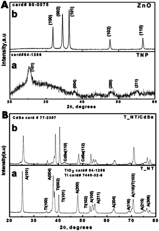 | ||
| Fig. 1 The surface characterization using XRD analysis of the (A, a) T_NP and (A, b) ZnO on glass slides and (B, a) T_NT and (B, b) T_NT–CdSe. | ||
TiCl4 treatment followed by annealing at 450 °C for 30 min forms anatase phase TiO2 nanoparticles (JCPDS card no 84-1286). Thus the formation of the respective oxides using the two treatment approaches is validated. The complete characterization of T_NT is discussed elsewhere.24 The additional peaks other than the anatase phase can be assigned to the Ti background (JCPDS card #7440-32-6). The CdSe deposits can be identified as cubic forms with (110) and (112) peaks (JCPDS card# 77-2307) as shown in Fig. 1B.
The optical absorption spectra can be used to distinguish the difference between TiO2 nanoparticles and unique features of T_NT samples as shown in Fig. 2A. TiO2 has a bandgap of 3.2 eV and therefore cannot absorb in the visible region of the solar spectrum and consequently appears white. However most T_NTs appear off-white (from yellow to blue depending on the annealing condition or defects introduced during synthesis such as Tin+ states and oxygen vacancies25). This change in absorbance in clearly noticed in the DRUV-Vis absorbance spectra of the treated T_NT samples. The as-prepared T_NT arrays appear muddy yellow and absorbance spectra indicate a distinct onset at ∼380 nm corresponding to their bandgap of 3.2 eV and a broad absorbance band centered at ∼500 nm.
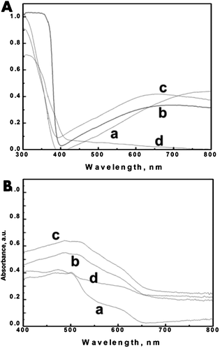 | ||
| Fig. 2 The absorbance spectra of (A, a) T_NT, (A, b) T_NT–T_NP, (A, c) T_NT–ZnO, and (A, d) T_NT–H2O2 and (B, a) T_NT–CdSe, (B, b) T_NT–T_NP–CdSe, (B, c) T_NT–ZnO–CdSe, and (B, d) T_NT–H2O2–CdSe. | ||
After annealing at 450 °C for 2 hours in air it darkens to a bluish color with the band center showing a slight redshift. This absorbance feature does not change with TiCl4 or Zn(NH3)42+ treatment. It has been shown elsewhere that the absorbance band appearing at <600 nm can be ascribed to O vacancy in the bulk and surface of metal oxide framework whereas the presence of Tin+ is responsible for absorbance >600 nm (ref. 26). This suggests that mainly oxygen vacancies are responsible for the band in as-prepared T_NT arrays but darkening of the samples with annealing converts them partially to Ti3+ states.
The outcome of the treatment of these samples in basic hydrogen peroxide is also shown in Fig. 2A. It indicates that hydrogen peroxide can bleach the T_NT close to an almost white color. Note that there is no significant absorbance in the visible part of the spectrum. This observation points to the reduction and possibly complete removal of the Tin+ states. ESI S3† provides the photographs of the T_NT before and after the surface treatment using all these methods.
Fig. 2B shows the DRUV-Vis absorbance spectra of the untreated and treated T_NT samples followed by CdSe deposition. The clear indication of visible light absorbance by all the samples confirms the XRD results which conclude that CdSe deposits are present on the T_NT. All the samples show an absorbance in the visible range confirming the deposition of CdSe. The T_NT–T_NP and T_NT–ZnO show almost similar absorbance traces. The H2O2 treated samples show a very small absorbance in the visible region, suggesting limited loading of CdSe. ESI S3† also provides the photographs of the samples after CdSe deposition.
The surface morphology of all the samples was examined using SEM. Representative images of the samples are compiled together and are shown in ESI S4.† The key highlights from the analysis of the SEM images are discussed below. The TiCl4 and Zn(NH3)42+ treatments result in the formation of discontinuous islands of nanoparticle clusters as an overlayer with higher surface roughness on T_NT. The clusters are noted to contain particles of size ranging from 5–10 nm for TiO2 and 15–20 nm for ZnO. These particles facilitate better loading of the CdSe compared to pristine T_NT. H2O2 bleached T_NTs are partly corroded with thinned walls and did not demonstrate very good CdSe adherence. In fact it shows lesser CdSe loading and corroborates the observations made during the spectroscopic analysis.
The effects of the two treatment methods applied to the T_NT were examined using three mutually complementing approaches including electrochemical (Mott Schottky), photoelectrochemical (chronopotentiometry), and optical (absorbance). Mott-Schottky (MS) analysis can be used to provide fundamental insights into the flatband potential and charge carrier density in a film. In this work the application of the MS technique is limited to determining the changes in the flat band potential of the T_NT-based samples before and after treatment. A larger or more negative flatband potential suggests better band bending resulting in an improved charge separation, while an increase in carrier density can be attributed to a greater presence of surface states. Fig. 3A shows the MS plots of T_NT with the T_NP and ZnO. A thermal annealing at 450 °C is required to form TNP and ZnO deposits after the TiCl4 and Zn(NH3)42+ treatment respectively. Following heat treatment, the flat band potential is observed to be −0.34 V with both oxides. Alternately, the MS plot of the T_NT after chemical treatment with H2O2 (Fig. 3B) shows a flat band potential at −0.47 V. The base line T_NT samples are annealed at two temperatures, 350 °C and 450 °C. Note that the T_NT shows flat band potentials of −0.39 V and −0.362 V (Table 1). It is also worth mentioning that dual slopes in the MS plots of all the electrodes can be observed, as marked in Fig. 3A and B. These slopes are attributable to the overlying hollow nanotube structure and the underlying compact oxide layer in between the nanotube and the Ti base.
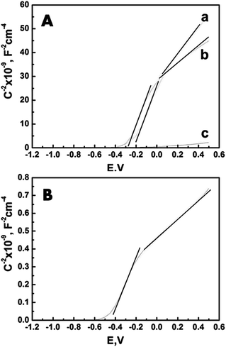 | ||
| Fig. 3 The results of the Mott Schottky analysis of (A, a) T_NT–T_NP, (A, b) T_NT–ZnO, (A, c)T_NT, and (B) T_NT–H2O2 performed in a 0.1 M aqueous solution of tetrabutyl ammonium hydroxide (TBAH) as the electrolyte. | ||
| Electrode | Flatband potential | Photo-voltage |
|---|---|---|
| T_NT (350C) | −0.39 V | 0.54 V |
| T_NT (450C) | −0.36 V | |
| T_NT–TNP | −0.34 V | 0.58 V |
| T_NT–ZnO | −0.34 V | 0.55 V |
| T_NT–H2O2 | −0.47 V | 0.52 V |
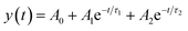
Photoelectrochemical measurements were performed by illuminating the samples with UV-vis light. Upon photo-illumination an instantaneous response is noted via an increase in the potential. Table 1 lists the values of the photovoltage measured after the increase in potential stabilizes. T_NT shows a photovoltage of 0.54 V. TNP or ZnO formation causes an increase in the photovoltage while the H2O2 treatment results in a decrease in photovoltage with respect to the untreated T_NT. Once illumination is turned off, a decay in the photovoltage is noted. The decay rate is a good measure of the presence of trap states in the photoanode material. Since a rapid decay is indicative of lower trap sites, the average time was estimated by fitting an exponential with two time constants to the V–t profile of each sample once the illumination is switched off. These values are estimated using the exponential relationship shown in eqn (1) and (2):
 | (1) |
| τm = (τ1τ2)/(τ1 + τ2) | (2) |
A simple optical approach to track the effects of electron trapping/detrapping in particulate films and TiO2 solutions consists of monitoring the color change. For example, a bluish color is generally indicative of electron trapping as per eqn (3):
 | (3) |
Along the same lines, the treatment effects applied on T_NT can also be co-related to the color of the samples (ESI Fig. S3†). It is known that heat treatment can cause such trap sites to increase.27 In fact, after heat treatment the change in the color of T_NT to a bluish tinge provides evidence for this effect. The deposition of ZnO or T_NP does not result in any change in color, indicating that it does not cause any trap sites to be passivated. Alternately, an H2O2 treatment results in the transformation of this bluish tinge to a white color. To further qualitatively corroborate the color effects, a closer examination of the absorbance onset was carried out. The absorbance shows almost complete removal of the absorption band in the visible region with H2O2 treatment and no shift with the T_NP or ZnO deposits.
Thus, the MS, chronopotentiometry, and absorbance studies provide the following results. First, the presence of oxides shows a shift of ∼50 mV towards the positive direction in the values of the flat band potential compared to the baseline material T_NT, while the H2O2 treatment results in a negative shift. Second, the chronopotentiometry results indicate a higher open circuit potential with the deposition of the secondary layer while the H2O2 treatment results in a decrease in photovoltage with respect to the base T_NT. Third, the absorbance studies indicate that H2O2 treatment results in passivation of the surface states while the addition of oxides does not make any significant alternations to the surface states. A schematic summarizing these observations, particularly indicating the effects of oxide treatment on the energetics of the composite, is shown in Fig. 4.
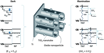 | ||
| Fig. 4 (Left) The schematic illustrates the change in the Fermi-levels (Ef1, Ef2) of the electrodes as a result of the shallow (ets) and deep (etd) surface states and (right) the UV-vis illumination of the different electrodes creates photogenerated charge pairs (e–h) that results in a change in the open circuit potential (ΔV1, ΔV2). | ||
The electron pumping using an external source (as it occurs in MS analysis) elevates the overall Fermi level towards the conduction band. However, the movement of the Fermi level is limited by the (i) presence, (ii) extent, and (iii) position of the surface states (ets,etd) below the conduction band giving rise to the different flat band potential for the differently treated samples. In the case of H2O2 the lower photovoltage and partial flaking of T_NT (as shown in ESI S4†) are indicative of a weak interface between the T_NT base and the underlying compact oxide. However, the H2O2 treated T_NT can be potentially beneficial once it is removed from the substrate and used (as a stand-alone membrane or as a layer deposited on another substrate such as an ITO glass plate).
Next, the presence of an overlying layer on the photoelectrochemical properties of bare- and treated T_NT were examined. The T_NTs were used as substrates for depositing a representative visible light harvesting agent: the chalcogenide CdSe. The successive ionic layer adsorption and reaction (SILAR) method was used to form the chalcogenide (ESI S1†). CdSe forms as a result of the electrostatic interaction between the Cd2+ and Se2− counter ions when the T_NT is dipped alternately into the respective salt solutions.28 Varying density of the CdSe coating can be prepared by simply repeating the SILAR process multiple times, leading to a high degree of surface coverage. Fig. 5A shows the current–voltage (J–V) characteristics of the various electrodes prepared by deposition of CdSe nanoparticles. The bare T_NT–CdSe nanotubes showed a current density of 2.4 mA cm−2. The T_NT–T_NP–CdSe electrodes show the highest photocurrent of ∼4.3 mA cm−2 and the largest zero current potential among all the T_NT electrodes. This was followed by ZnO, bare T_NT, and H2O2 treated T_NT. The time dependent photocurrent and photovoltage response of the electrodes were examined as well and are shown in Fig. 5B and C. These experiments were repeated several times and an average of the multiple runs are reported in the table shown in Table 2. It should be noted that the mean deviation in the data is ±5%. Since the photoelectrochemical results are of relevance in photovoltaic applications, of key interest is the relative trend in the magnitudes of the photocurrent in these electrodes. To this end, the effects of the CdSe presence on the various T_NTs indicate the following order: JT_NT–TiO2–CdSe > JT_NT–ZnO–CdSe > JT_NT–CdSe > JT_NT–H2O2–CdSe.
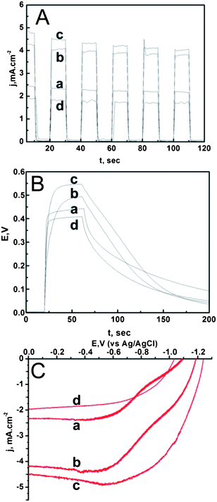 | ||
| Fig. 5 The photoelectrochemical measurements performed on the T_NT after CdSe deposition include (A) voltammetry (J–V), (B) chronoamperometry (J–t), and (C) chronopotentiometry (V–t). Each of these graphs shows the responses of (a) T_NT–CdSe, (b) T_NT–T_NP–CdSe, (c) T_NT–ZnO–CdSe, and (d) T_NT–H2O2–CdSe electrodes in the presence of 0.1 M aqueous tetrabutyl ammonium sulfide (TBAS) as the electrolyte performed under UV-vis illumination. | ||
| Electrode | Na2S | TBAS | ||
|---|---|---|---|---|
| V oc | J sc | V oc | J sc | |
| T_NT | 0.33 | 4.19 | 0.45 | 2.34 |
| T_NT–TNP | 0.39 | 8.86 | 0.55 | 4.68 |
| T_NT–ZnO | 0.37 | 8.44 | 0.49 | 4.15 |
| T_NT–H2O2 | 0.27 | 1 | 0.41 | 1.97 |
It is well understood that photogenerated electrons produced by visible light absorbance in the conduction band of the CdSe are injected into the conduction band of TiO2 using the following staircase-type hoping mechanism as shown in eqn (4):
CdSe(ecb) + TiO2 ![[thin space (1/6-em)]](https://www.rsc.org/images/entities/char_2009.gif) → CdSe + TiO2(ecb) → CdSe + TiO2(ecb) | (4) |
Under this scenario, it is reasonable to expect that the varying levels of trap states in the T_NT can potentially alter the path and/or the mobility of these externally injected electrons. However the V–t results of the treated T_NT (Table 1) and the V–t results after CdSe deposition on the treated T_NT (Table 2) demonstrate a similar trend. In general, photoelectrochemical response is adversely affected by H2O2 treatment while the oxide deposits are noted to improve it. This observation qualitatively indicates that the externally produced electrons are minimally affected by the alternations at the T_NT surface. Further, higher voltages (and photocurrent) are noted in the presence of oxide deposits. The oxide deposits on the T_NT surface favorably promote an increase in the dispersion of the chalcogenide, resulting in this observed outcome. ESI S5† provides a schematic of the relative energy levels and the corresponding electron transfer mechanism.
Another key aspect that influences the photoelectrochemical properties is the electrolyte. The electrolyte effect, specifically its dimensions and the charge associated with it, can determine the extent of redox activity at the electrode–electrolyte interface. In fact, it is reported that Na2S interferes with T_NT while the tetrabutyl ammonium ion of tetrabutyl ammonium sulfide (TBAS) has a significantly reduced intercalation in T_NT by virtue of its larger cation size.13 The article further goes on to describe that the use of TBAS allows for determining the true effects of the electrode on a photoelectrochemical process. Since the T_NT surface treatment effects are of primary interest in this work, it is pertinent to avoid any other interference such as ion intercalation (should they exist). With this objective, a TBAS was synthesized with modification of an earlier reported method29 and used as an electrolyte to test the photoelectrochemical responses of the various electrodes. The results of this comparative analysis are shown in Table 2. This preliminary experiment demonstrates that not only the trends in the photoelectrochemical responses are similar in the presence of both electrolytes but also the absence of any potential interference from the Na+ (lower size) allows for deciphering the true magnitudes of the photoelectrochemical response. Further work is needed to understand the reasons for these effects and the complete potential of alternate electrolytes and the viability of such replacements in an actual photocell configuration.
Conclusions
Surface treatment of T_NT, a critical step that influences photovoltaic, photoluminescence, and photocatalytic properties, has been examined using two approaches, viz., treatment with oxide precursors and peroxide. The treatment effects have been systematically probed using complementary surface, electrochemical, photoelectrochemical, and optical studies. Using an oxide precursor results in the formation and distribution of respective oxide nanoparticles (ϕ = 5–10 nm for TiCl4 treatment and 15–20 nm for Zn(NH3)42+ treatment respectively) on the T_NT. An increase of 7.4% and 1.8% in photovoltage compared to untreated T_NT is noted with T_NP and ZnO respectively. Alternately, peroxide treatment results in the passivation of the surface states but destabilization of the base leading to a reduction in photocurrent and photovoltage. Finally, the performance of the treated T_NT with an overlying representative chalcogenide deposit (for visible light absorption) has been studied. Photocurrent (photovoltage) values of 4.68 mA (0.549 V), 4.15 mA (0.490 V), and 2.34 mA (0.445 V) are noted with TiCl4, Zn(NH3)42+ and bare T_NT with CdSe respectively.Acknowledgements
This work was made possible due to the funding from the Department of Energy. RSV would also like to thank the Office of the Vice-President for Research for partial support. The funding from DOE through grant DE-EE0000272 is also appreciated.References
- J. M. Macak, H. Tsuchiya, A. Ghicov, K. Yasuda, R. Hahn, S. Bauer and P. Schmuki, Curr. Opin. Solid State Mater. Sci., 2007, 11, 3–18 CrossRef CAS.
- P. Roy, S. Berger and P. Schmuki, Angew. Chem., Int. Ed., 2011, 50, 2904–2939 CrossRef CAS.
- G. K. Mor, O. K. Varghese, M. Paulose, K. Shankar and C. A. Grimes, Sol. Energy Mater. Sol. Cells, 2006, 90, 2011–2075 CrossRef CAS.
- G. M. Turner, M. C. Beard and C. A. Schmuttenmaer, J. Phys. Chem. B, 2002, 106, 11716–11719 CrossRef CAS.
- S. Liang, J. He, Z. Sun, Q. Liu, Y. Jiang, H. Cheng, B. He, Z. Xie and S. Wei, J. Phys. Chem. C, 2012, 116, 9049–9053 CAS.
- V. K. Mahajan, M. Misra, K. S. Raja and S. K. Mohapatra, J. Phys. D: Appl. Phys., 2008, 41, 125307 CrossRef.
- K. Shankar, J. I. Basham, N. K. Allam, O. K. Varghese, G. K. Mor, X. Feng, M. Paulose, J. A. Seabold, K.-S. Choi and C. A. Grimes, J. Phys. Chem. C, 2009, 113, 6327–6359 CAS.
- O. K. Varghese, M. Paulose and C. A. Grimes, Nat. Nanotechnol., 2009, 4, 592–597 CrossRef CAS.
- D. Wang, Y. Liu, B. Yu, F. Zhou and W. Liu, Chem. Mater., 2009, 21, 1198–1206 CrossRef CAS.
- J. R. Jennings, A. Ghicov, L. M. Peter, P. Schmuki and A. B. Walker, J. Am. Chem. Soc., 2008, 130, 13364–13372 CrossRef CAS.
- K. Zhu, N. R. Neale, A. Miedaner and A. J. Frank, Nano Lett., 2006, 7, 69–74 CrossRef.
- A. Muñoz, Q. Chen and P. Schmuki, J. Solid State Electrochem., 2007, 11, 1077–1084 CrossRef.
- F. Fabregat-Santiago, E. M. Barea, J. Bisquert, G. K. Mor, K. Shankar and C. A. Grimes, J. Am. Chem. Soc., 2008, 130, 11312–11316 CrossRef CAS.
- C. Richter and C. A. Schmuttenmaer, Nat. Nanotechnol., 2010, 5, 769–772 CrossRef CAS.
- B. C. O'Regan, J. R. Durrant, P. M. Sommeling and N. J. Bakker, J. Phys. Chem. C, 2007, 111, 14001–14010 CAS.
- P. M. Sommeling, B. C. O'Regan, R. R. Haswell, H. J. P. Smit, N. J. Bakker, J. J. T. Smits, J. M. Kroon and J. A. M. van Roosmalen, J. Phys. Chem. B, 2006, 110, 19191–19197 CrossRef CAS.
- S. Wu, H. Han, Q. Tai, J. Zhang, B. L. Chen, S. Xu, C. Zhou, Y. Yang, H. Hu and X.-Z. Zhao, Appl. Phys. Lett., 2008, 92, 122106–122108 CrossRef.
- X.-L. Yu, J.-G. Song, Y.-S. Fu, Y. Xie, X. Song, J. Sun and X.-W. Du, J. Phys. Chem. C, 2010, 114, 2380–2384 CAS.
- C. Chen, X. Yi, A. Ghafar, Y. Seung Hwa and C. Sung Oh, Nanotechnology, 2011, 22, 015202 CrossRef.
- S. H. Kang, J.-Y. Kim, Y. Kim, H. S. Kim and Y.-E. Sung, J. Phys. Chem. C, 2007, 111, 9614–9623 CAS.
- C. Rho, J.-H. Min and J. S. Suh, J. Phys. Chem. C, 2012, 116, 7213–7218 CAS.
- J. Wang and Z. Lin, Chem. Mater., 2009, 22, 579–584 CrossRef.
- Y. R. Smith and V. Subramanian, J. Phys. Chem. C, 2011, 115, 8376–8385 CAS.
- Y. S. Sohn, Y. R. Smith, M. Misra and V. Subramanian, Appl. Catal., B, 2008, 84, 372–378 CrossRef CAS.
- Y.-C. Nah, I. Paramasivam and P. Schmuki, ChemPhysChem, 2010, 11, 2698–2713 CrossRef CAS.
- V. N. Kuznetsov and N. Serpone, J. Phys. Chem. C, 2009, 113, 15110–15123 CAS.
- S. P. Albu, H. Tsuchiya, S. Fujimoto and P. Schmuki, Eur. J. Inorg. Chem., 2010, 4351–4356 CrossRef CAS.
- H. J. Lee, J. Bang, J. Park, S. Kim and S.-M. Park, Chem. Mater., 2010, 22, 5636–5643 CrossRef CAS.
- L. Li, X. Yang, J. Gao, H. Tian, J. Zhao, A. Hagfeldt and L. Sun, J. Am. Chem. Soc., 2011, 133, 8458–8460 CrossRef CAS.
Footnote |
| † Electronic supplementary information (ESI) available. See DOI: 10.1039/c2nr31660a |
| This journal is © The Royal Society of Chemistry 2013 |