DOI:
10.1039/C3LC50922B
(Paper)
Lab Chip, 2014,
14, 237-243
Nanoslit membrane-integrated fluidic chip for protein detection based on size-dependent particle trapping†
Received
7th August 2013
, Accepted 17th October 2013
First published on 18th October 2013
Abstract
This paper describes the fabrication of a nanoslit membrane-integrated fluidic chip (Nanoslit-Chip) used for trapping and concentrating micro-/nano-particles of desired size and its application in detecting biological molecules based on target-induced particle aggregation. To trap particles of a specific size, a large scale uniform sized nanoslit fluid channel array is fabricated on a silicon dioxide membrane. A small number of fluorescence labeled particles in a large volume of solution are concentrated into a monolayer of particles in a small nanoslit membrane, which enables us to effectively quantify them via fluorescence intensity. In addition, the particles of desired size (1.8 μm) are readily separated from the mixture of particles with a different size (450 nm) in Nanoslit-Chip size, and then quantified via fluorescence measurements. Finally, the Nanoslit-Chip is successfully applied to the sensitive detection of proteins by target-induced particle aggregation, trapping, and quantification. This shows its potential as a biological and clinical device for quantitative and sensitive detection of biological molecules.
Introduction
Nanoparticle-based assays have received a lot of attention for the in vitro detection of target molecules because its unique properties allow signal amplification for sensitive detection.1–4 The critical issues in nanoparticle-based assays are the spatial localization, separation, and concentration of a very small subpopulation of interesting nanoparticles that bear target molecules for sensitive and quantitative detection.5 One conventional method for separating and concentrating a nanoparticle–target complex is magnetic separation using magnetic micro/nanoparticles.6–11 Magnetic separation and concentration have the advantages of being simple and quick to isolate, as well as being easy to integrate into microfluidic devices. However, the magnetic particles are limited to concentration in very small areas, and signal collections are hindered by the inhomogeneous mixture of the probe nanoparticles and magnetic particles for ultra-sensitive detection.9,12 Therefore, effective strategies for the separation and concentration of nanoparticle–target complexes in a small area remain important for sensitive and quantitative analysis.
Nanofluidic devices that are integrated with nanostructures including channels, pores, and slits become promising platforms for handling nanoparticles and biological samples that can be spatially confined.13–15 The cross-section in nanostructures allows subpopulation collection from a polydispersed mixture after passing through the nanochannels.16,17 So far, various nanofluidic devices have been developed with various materials and structures.18,19 In terms of the types of physical structures, nanochannels are classified into horizontal and vertical ones. A horizontal nanochannel has a parallel orientation to its substrate surface while a vertical nanochannel has a vertical orientation. Horizontal nanochannels are not suitable for a nanoparticle-based assay due to low fluid transport and non-specific clogging of the nanochannels by nanoparticles.15,19,20 The flow resistance of nanofluidic devices is determined by the total cross sectional area and dimensions of nanochannels.21 The total cross sectional area of a horizontal nanochannel is generally very small because the nanochannel can be fabricated only in one-dimensional arrays on the substrate surface. Vertical nanofluidic devices could solve the issues faced by horizontal devices. A large number of vertical nanochannels can be fabricated in a two-dimensional array, which allows a fluid to flow through the nanochannels with low flow resistance. Various high resolution lithography technologies have been reported to fabricate nanochannels such as electron beam lithography (EBL),22,23 focused ion beam (FIB) milling,24,25 and nano-imprint lithography (NIL).26,27 The high resolution lithography technologies are able to fabricate precise and reliable nanochannels, but they require high costs and long fabrication times for patterning a large number of nanochannels. Polymer-based nanochannels have been fabricated by using the polymer's deformability. However, this approach can produce only horizontal nanochannels.13,28 Anodic aluminium oxide (AAO) is one of the useful technologies for fabricating vertical nanochannel arrays.29–31 However, the shape is limited to circular patterns, and fabrication of a highly ordered nanopore array is limited to several micrometres without pre-patterning the aluminium.32 In addition, nanoslits with high aspect ratios are more desirable than nanopores in terms of large fluid transport and minimization of particle clogging. Therefore, there is a need to develop vertical nanochannels that have a uniform and size-controllable nanoslit array with low flow resistance for size-dependent separation and quantitative analysis of particles.
In this paper, we propose a nanoslit fluidic chip that has a nanoslit array membrane (Nanoslit-Chip) for trapping and concentrating particles of a desired size, as well as its application to the sensitive detection of biological molecules based on the target-induced aggregation of particles. The proposed device is comprised of a PDMS top fluid channel, a silicon dioxide nanoslit array membrane, and a silicon bottom fluid channel. The width of the nanoslit can easily be controlled in nanoscale by a chemical vapor deposition process of silicon dioxide to trap particles of a specific size from the mixture of polydispersed particles. The flow resistance in a Nanoslit-Chip is much lower than the one in horizontal nanochannels, since a Nanoslit-Chip consists of a large number of nanoslit arrays. Therefore, a large volume of samples can be accurately and continuously injected into the device using a syringe pump to concentrate the particles of a desired size. We demonstrate size-dependent trapping of fluorescent nanoparticles (450 nm)/microparticles (1.8 μm) and their quantitative analysis by measuring the fluorescence intensity in a Nanoslit-Chip. Finally, the Nanoslit-Chip was applied to the sensitive detection of BSA by trapping the target-induced particle aggregates. The target-bound nanoparticles were separated from the unbound ones and concentrated in the small nanoslit array, which leads to sensitive and quantitative detection of biomolecules (ten picomolar concentration).
Design and fabrication
Design of Nanoslit-Chip for size-dependent trapping and concentration of particles
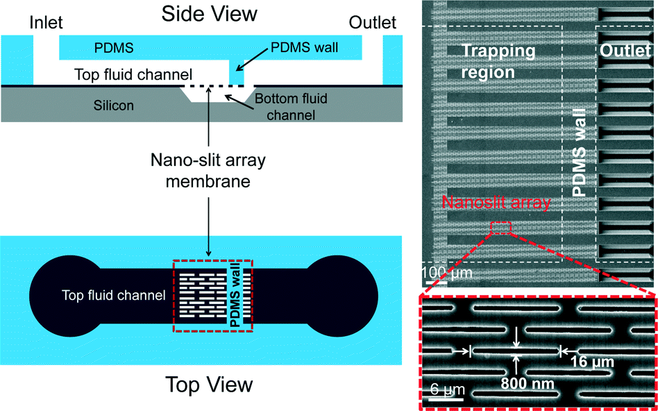
The design of a Nanoslit-Chip is shown in Fig. 1. The Nanoslit-Chip consists of a PDMS top fluid channel, a silicon bottom fluid channel, and a silicon dioxide nanoslit array membrane that is located between the PDMS top channel and the silicon bottom channel. A polydispersed nanoparticle fluid mixture flows through the nanoslit array membrane where particles larger than the width of the nanoslit are trapped. The wall of the PDMS top fluid channel was designed to guide the fluid from the top fluid channel to the nanoslit membrane. The width and height of the PDMS top fluid channel are 1 mm and 50 μm, respectively. The width of the nanoslit is controllable in the range from 2 μm to 250 nm using a deposition process of silicon dioxide, while the length is 16 μm. A large number of nanoslits (~4300) are located in the nanoslit array membrane (1 mm × 0.8 mm). The controllable array membrane can accommodate a large fluid volume with low pressure to pass through the nanoslit because the hydraulic resistance (Rhydraulic) of the nanoslit membrane is reduced by increasing the number of nanoslits. The Rhydraulic of the nanoslit membrane is described as follows:| | 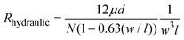 | (1) |
where N is the number of nanoslits; μ is fluid viscosity; and d, l, and w are the depth, length, and width of the nanoslit, respectively. The volumetric flow rate (Qflow rate) is simply calculated by Qflow rate = Rhydraulic × P, and the required pressure was lower than 10 kPa for 100 μl min−1. The required pressure of the nanoslit membrane is about one thousand times lower than that of the horizontal nanochannel, which has similar dimensions. (The hydraulic resistance calculation and the required pressure for the volume flow of the nanoslit membrane and the horizontal nanochannel are shown in Fig. S1, ESI.†)
 |
| | Fig. 1 Schematics of the nanoslit membrane-integrated fluidic chip (Nanoslit-Chip) (left) and SEM images of the nanoslit membrane region which has a nanoslit array for particle trapping (right). The width, length, and height of the nanoslit are 800 nm, 16 μm, and 2.5 μm, respectively. | |
Fabrication of Nanoslit-Chip with nanoslit array membrane
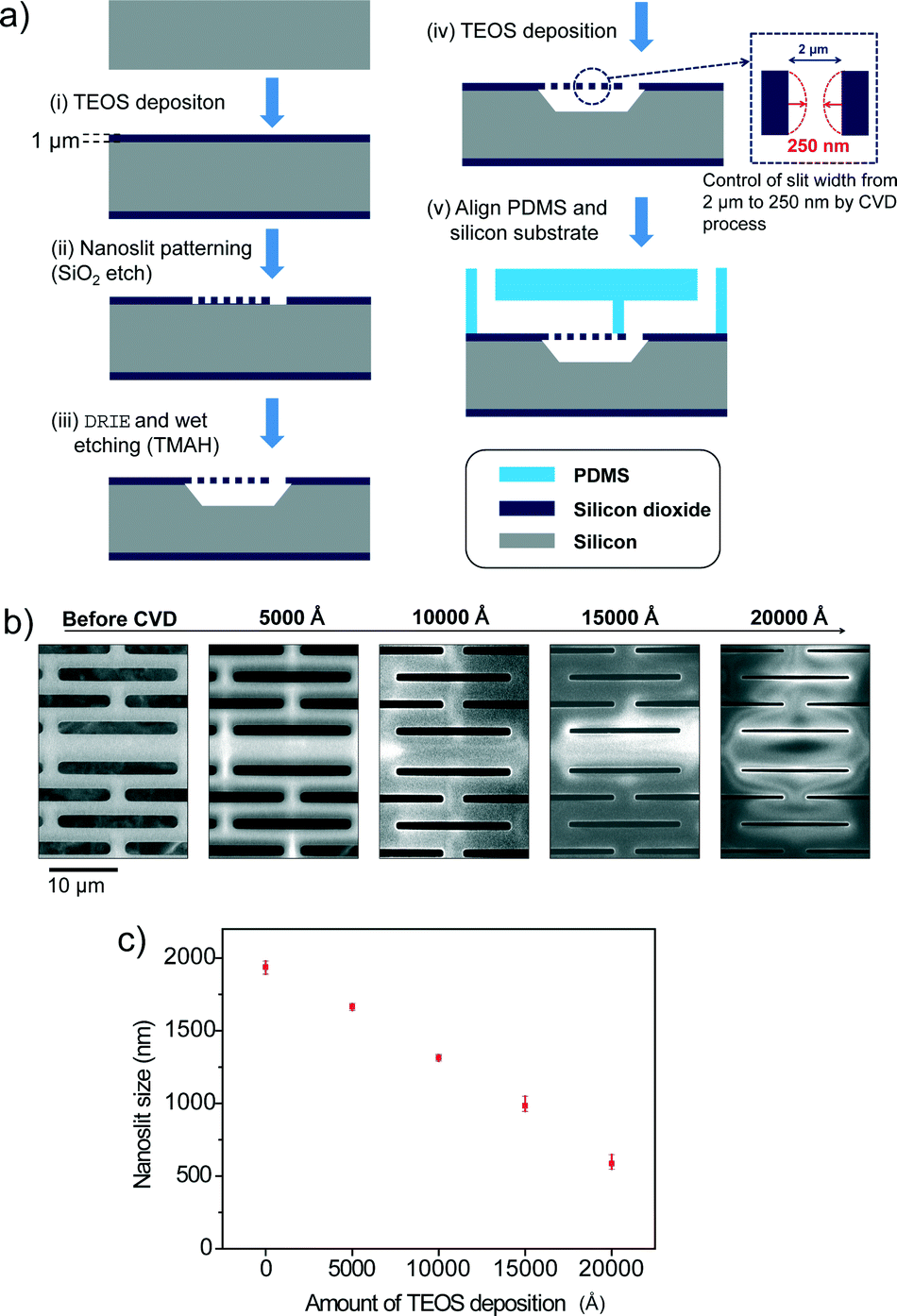
Fig. 2a shows the schematic diagram for the fabrication process of the Nanoslit-Chip. First, tetraethyl orthosilicate (TEOS) was deposited on the silicon wafer to form a thin film of silicon dioxide (1 μm physical thickness). Then, the nanoslits were patterned on the silicon dioxide layer by photolithography and a dry etching process. The silicon layer was etched using deep reactive ion etching (DRIE) and tetramethylammonium hydroxide (TMAH) wet etching processes to fabricate the nanoslit membrane and the bottom fluid channel. The TEOS deposition (Applied Material, Precision 5000) reduced the slit size from 2 μm to the target slit size, as shown in process (iv) of Fig. 2a. The target slit size was 800 nm for the selective trapping of larger ones from a mixture of 1.8 μm and 450 nm particles. Fig. 2b and c show the sizes of the nanoslit widths during the TEOS deposition process. The slit widths were reduced linearly by the TEOS deposition process, which indicates that the slit width can be precisely and easily controlled by TEOS deposition. A PDMS top fluid channel was fabricated using soft lithography. First, SU-8 photoresist was patterned on a silicon wafer using photolithography for PDMS molding. A PDMS pre-polymer (Sylgard 184 A) was mixed with the curing agent (Sylgard 184 B) at a 10![[thin space (1/6-em)]](https://www.rsc.org/images/entities/char_2009.gif) :1 (v/v) ratio and poured on the SU-8 patterned silicon wafer. Then, the PDMS mixture was degassed in a vacuum chamber and cured in an oven at 70 °C for 4 hours. Finally, the PDMS top substrate containing the top fluid channel was aligned with the nanoslit membrane and clamped by an acrylic plastic housing. The fabrication process of the Nanoslit-Chip is very simple, inexpensive, and suitable for mass production, as opposed to the high resolution lithography technologies, because the Nanoslit-Chip only requires standard photolithography and the TEOS chemical vapor deposition process. We tried to reduce the nanoslit size from 2 μm to 250 nm using the deposition process. However, reduction of the slit width was limited by the stress of the membrane material (silicon dioxide). The deformation of the membrane can be reduced by using silicon nitride, which has tensile stress. (The fabrication results and SEM images are shown in Fig. S2, ESI.†)
:1 (v/v) ratio and poured on the SU-8 patterned silicon wafer. Then, the PDMS mixture was degassed in a vacuum chamber and cured in an oven at 70 °C for 4 hours. Finally, the PDMS top substrate containing the top fluid channel was aligned with the nanoslit membrane and clamped by an acrylic plastic housing. The fabrication process of the Nanoslit-Chip is very simple, inexpensive, and suitable for mass production, as opposed to the high resolution lithography technologies, because the Nanoslit-Chip only requires standard photolithography and the TEOS chemical vapor deposition process. We tried to reduce the nanoslit size from 2 μm to 250 nm using the deposition process. However, reduction of the slit width was limited by the stress of the membrane material (silicon dioxide). The deformation of the membrane can be reduced by using silicon nitride, which has tensile stress. (The fabrication results and SEM images are shown in Fig. S2, ESI.†)
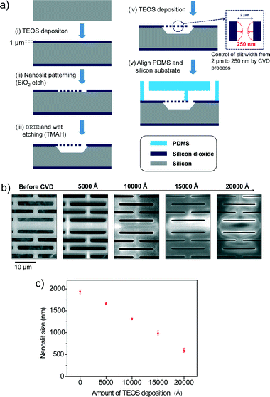 |
| | Fig. 2 a) Fabrication process of the Nanoslit-Chip. (i) TEOS deposition for nanoslit membrane, (ii) nanoslit array patterning by photolithography and SiO2 etch, (iii) DRIE and wet etching for bottom fluid channel, (iv) TEOS deposition to reduce the slit size in the range from 2 μm to 250 nm, and (v) alignment of PDMS top substrate with the silicon bottom substrate. b) SEM images showing the size reduction of the nanoslit width during the TEOS deposition process (iv) and c) nanoslit widths according to the amount of TEOS deposition. | |
Strategy for size-dependent trapping and concentration of particles in the Nanoslit-Chip
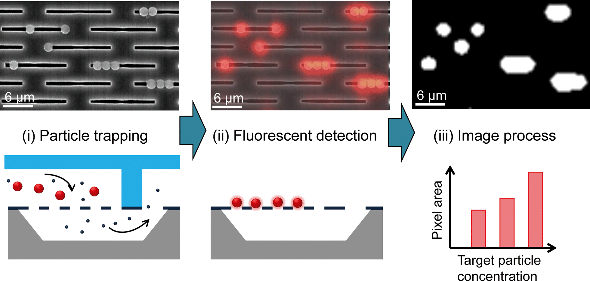
The strategy for the size-dependent trapping, concentration and quantitative analysis of particles is shown in Fig. 3. First, the two different-sized particles were flown into the nanoslit array membrane; the larger particle is 1.8 μm (red fluorescence) while the other is 450 nm (blue fluorescence). Particles larger than the nanoslit width are trapped on the nanoslit array membrane while the smaller ones can pass through to the bottom fluid channel. The trapped particles appear to form a monolayer on the nanoslit array membrane because a large number of nanoslit arrays prevent the formation of a multilayer until the injected particles exceed the number of nanoslits. The concentrated particles in the monolayer allow for their accurate quantification. Fluorescence microscopy is used to quantify the fluorescence signals of the trapped particles in the nanoslit membrane. The background noise of the fluorescence image was removed, and the total pixel area for the trapped particles was measured using image analysis software (NI Vision Assistant). The same fluorescence image area was then observed using FE-SEM to confirm the number of particles, which is correlated with the fluorescence intensity.
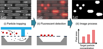 |
| | Fig. 3 Process for size-selective particle separation and fluorescence analysis. (i) Size-selective particle separation. (ii) Fluorescence detection of the trapped particles on a nanoslit membrane. (iii) Image processing for quantitative analysis of the trapped particles. | |
Apparatus
A microsyringe pump was used for continuous flow injection (Harvard PHD 2000, Harvard Apparatus, Holliston, MA, USA). Real time fluid motions were monitored using a CCD camera-linked optical microscope (ProgRes C3, JENOPTIK, Germany). Fluorescence measurements were performed using a fluorescence stereomicroscope (Leica M165 FC, Leica, Germany). Cyan fluorescent protein (CFP) filter set (425–445 nm excitation wavelength) and Discosoma red fluorescent protein (DsRed) filter set (515–560 nm excitation wavelengths) were used to detect blue and red fluorescent particles, respectively.
Results and discussion
Particle trapping at the 800 nm nanoslit membrane
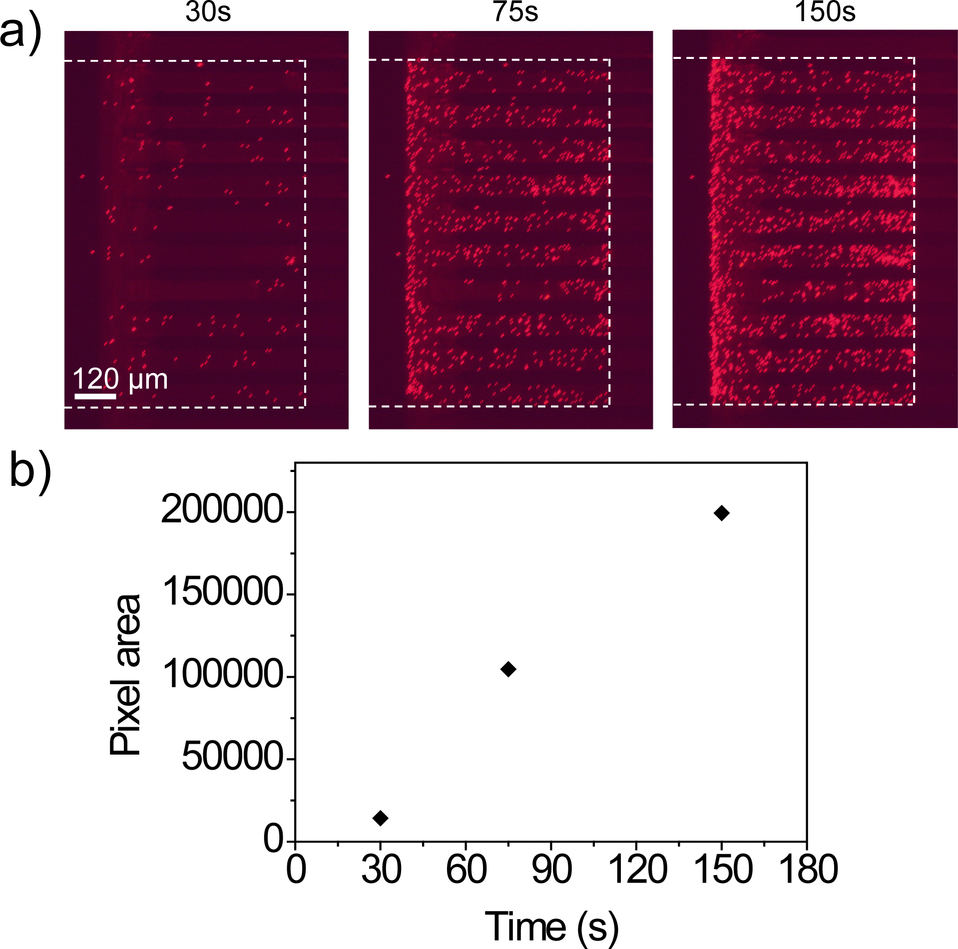
The trapping experiment for particles larger than the nanoslit width was performed in the Nanoslit-Chip. 1.8 μm sized particles that had a red fluorescent dye were prepared at 104 ml−1 concentration and injected into the Nanoslit-Chip at a flow rate of 40 μl min−1 for 150 s (total number of injected particles is approximately 103). Fluorescence images of the nanoslit membrane were acquired at each time interval during the sample injection, as shown in Fig. 4a. The red fluorescent signals were only observed in the trapping region (inside the white line) of the membrane, while no signal was observed in the region covered with the PDMS top substrate (outside the white line). The total red fluorescence intensity gradually increases as a function of injection time, indicating that the particles in the fluid are continuously injected into the nanoslits by overcoming the hydraulic resistance of the nanoslit membrane using a mechanical pump. The particles were stably trapped in the nanoslit membrane upon sample injection and in the following washing steps. Most of the particles were located in the nanoslit patterns and only a small portion of particles is non-specifically attached on the silicon oxide surface. Since the particles were trapped in a monolayer without stacking up, the total area of red pixels in the fluorescence image linearly increased as sample injection time increased (Fig. 4b). This result clearly indicates that the number of particles trapped in the nanoslit membrane can be quantified by counting the fluorescence areas. (For a movie of trapping the 1.8 μm red fluorescent particles in the membrane, see Movie S1, ESI.†)
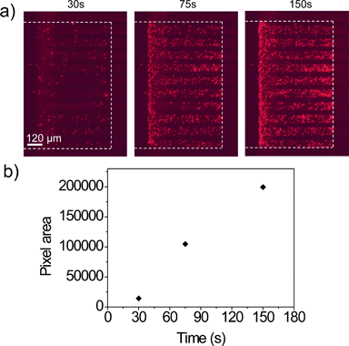 |
| | Fig. 4 a) Fluorescence images of the 800 nm nanoslit membrane during the trapping of 1.8 μm red fluorescent particles over the injection time. The white dotted line indicates the boundary of the trapping region and the PDMS wall. b) Red pixel area of particle trapped membrane in (a) over the injection times of 30, 75, and 150 s. (For a movie of trapping the 1.8 μm red fluorescent particles in the membrane, see Movie S1, ESI.†) | |
Quantitative analysis of particles trapped in Nanoslit-Chip
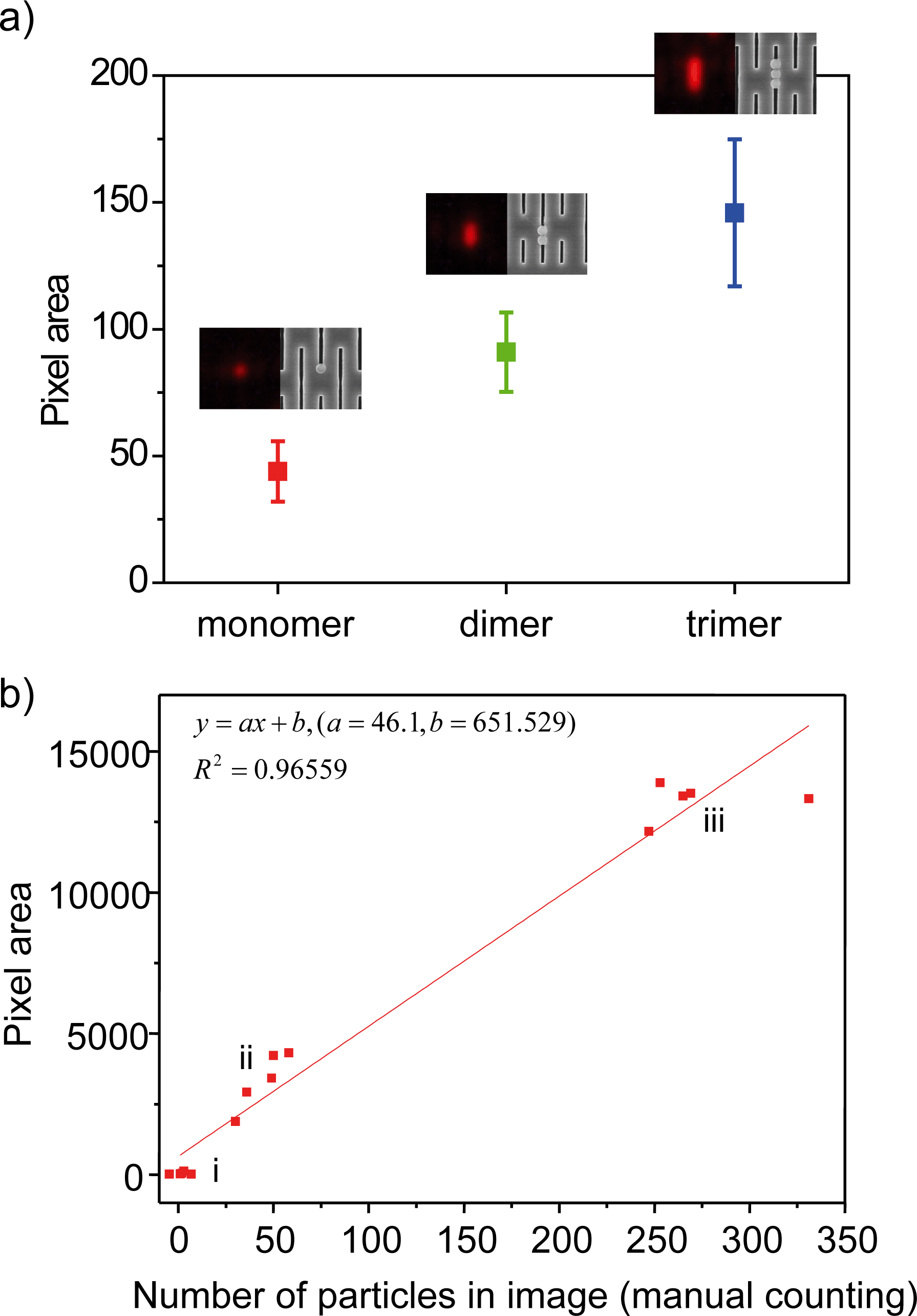
Quantitative analysis of particles trapped in the Nanoslit-Chip was performed using image processing. In order to confirm that the fluorescence pixel area corresponds to the number of particles, the number of trapped particles was counted using SEM after taking the fluorescence images of mono-, di-, and tri-particles. Fig. 5a shows that the fluorescence images of the particles match well with their SEM images, and the fluorescence area is proportional to the number of particles. This result indicates that the trapped particles can be quantified through fluorescence intensity.
 |
| | Fig. 5 a) Red pixel area for the monomer, dimer, and trimer of 1.8 μm red fluorescent particles that were trapped on the nanoslit membrane. The fluorescence and SEM images indicate trapped particle states. b) Relationship between the red pixel area and the number of trapped particles. The particles were manually counted in the SEM image and the red pixel area was obtained from the fluorescence image using image processing. The images were classified into 3 groups according to the concentrations of the injected particle. The concentration of the 1.8 μm particles was 103 ml−1 for group (i), 104 ml−1 for group (ii), and 105 ml−1 for group (iii), and the total injection volume of each sample was 100 μl. The equation is a linear fit of the comparison data. | |
Next, we trapped and quantified a large number of particles (103 ml−1, 104 ml−1, and 105 ml−1, respectively) using Nanoslit-Chip. The number of trapped particles in the five regions (85 μm × 64 μm) of the nanoslit membrane for each concentration was counted in SEM images before being compared to the red pixel area corresponding to the same region in the SEM analysis. (The fluorescence images and the corresponding SEM images in groups (i), (ii), and (iii) are shown in Fig. S3, ESI.†) A linear relationship between the red pixel areas and the number of particles was observed (the square of the correlation coefficient (R2) is 0.96559), as shown in Fig. 5b. The linearity was good at low and intermediate particle concentrations, but the variation was increased at high particle concentration due to the fluorescence intensity and the size variations of the multimer particles. This result shows that the Nanoslit-Chip is able to quantify the number of particles trapped in the nanoslit membrane, which is beneficial for a quantitative analysis of biological molecules.
Particle-induced clogging at the 800 nm nanoslit membrane
We investigated whether clogging of nanoslits by particles occurs, which could lead to non-specific trapping of undesired particles at the nanoslit membrane. Even particles smaller than the channel dimension could clog the nanoslits due to an increase in the particle density as the fluid channel dimension decreases.33,34 The particle concentration and the fluid channel dimension are the critical factors in particle-induced clogging. To examine particle-induced clogging in a 800 nm nanoslit array membrane, we prepared 450 nm blue fluorescent particles with three different concentrations (105 ml−1, 106 ml−1, and 107 ml−1, respectively). The particles were injected into the 800 nm nanoslit array membrane at a flow rate of 40 μl min−1 for 150 s. And then, the Nanoslit-Chip was washed using DI water at a flow rate of 40 μl min−1 for 150 s. After injection, washing, and drying, the nanoslit array membrane was analyzed via fluorescence measurements. Fluorescence images of the nanoslit membrane after filtration of the 450 nm particles are shown in Fig. 6a. When the particle concentration was 105 ml−1, a very small portion of the blue pixel area (lower than 0.06%) was observed. This result clearly indicates that particle-induced clogging did not occur at a concentration of 105 ml−1 and that most of the particles passed through the nanoslit array membrane. When the particle concentration was 106 ml−1, the blue pixel area increased to more than 7 times that of the 105 ml−1 concentration. This is attributed to the increased number of injected particles (10 times larger than 105 ml−1). The severe clogging of the nanoslit membrane by particles was observed at a concentration of 107 ml−1. The blue pixel area increased drastically (65 times larger than at 106 ml−1), which shows that the increased density of particles in the nanoslit region causes clogging at the initial stage. This prevents smaller particles from passing through the bigger nanoslits. As shown in Fig. 6b, the blue fluorescence area was quantitatively measured for each concentration. The blue pixel areas at the concentrations of 105 ml−1 and 106 ml−1 showed that particle-induced clogging rarely occurred. However, the blue fluorescence area at the concentration of 107 ml−1 dramatically increased due to particle-induced clogging. Based on these results, we found that there are optimal concentrations of particles for trapping and quantifying a specific size of particles for a specific nanoslit membrane.
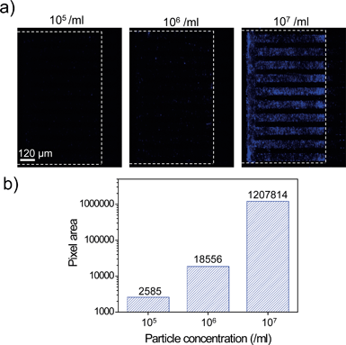 |
| | Fig. 6 a) Fluorescence images of the nanoslit membrane after the 450 nm blue fluorescent particles in different particle concentrations (105 ml−1, 106 ml−1, and 107 ml−1) were injected. The white dotted line indicates the boundary of the trapping region and the PDMS wall. b) Blue pixel area of particle trapped by the nanoslit membrane as a function of injected particle concentration. | |
Selective trapping of particles at the 800 nm nanoslit membrane
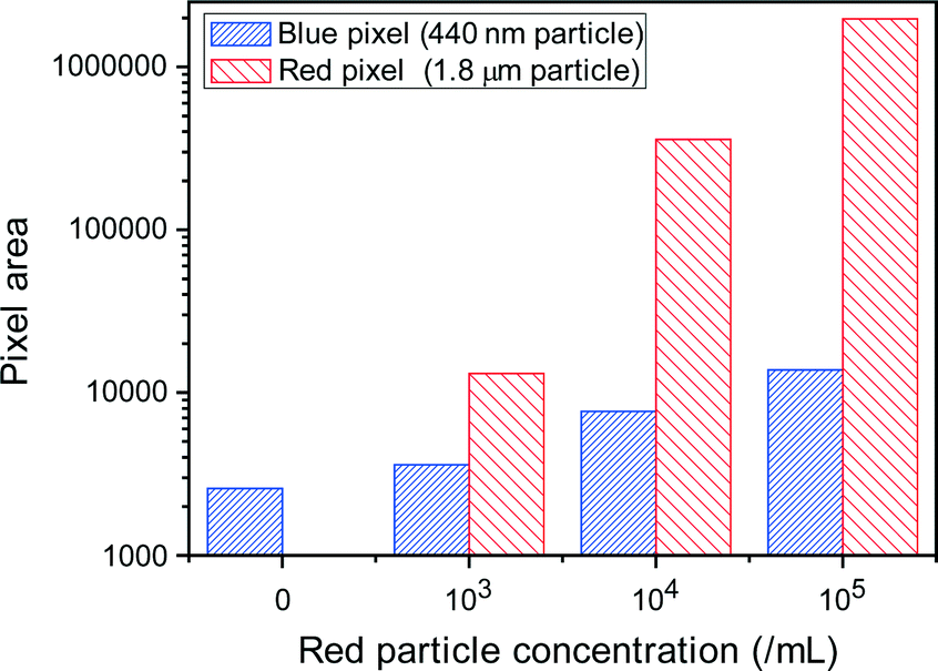
Next, specific particles were separated from the particle mixtures of different sizes using the Nanoslit-Chip. For size-selective trapping of particles, 1.8 μm sized red fluorescent particles and 450 nm sized blue fluorescent particles were mixed together at various particle concentrations. The concentrations of 1.8 μm particles varied from 0 to 103 ml−1, 104 ml−1, and 105 ml−1, while the concentration of the 450 nm particles was fixed at 105 ml−1. The particle mixtures were injected into the Nanoslit-Chip at a flow rate of 40 μl min−1 for 150 s. And then, the Nanoslit-Chip was washed using DI water and dried before fluorescence measurements. As shown in Fig. 7, the red pixel area for 1.8 μm particles proportionally increased with their concentration. However, the blue pixel area for 450 nm particles showed little increase even in the presence of a high concentration of 1.8 μm particles. This small increase in the blue fluorescence area at a high concentration of 1.8 μm particles is attributed to the decrease in open area in the nanoslit membrane, which means that 450 nm particles clog the membrane slightly. This result reveals that the Nanoslit-Chip is able to trap and concentrate a desired size of particles.
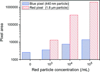 |
| | Fig. 7 Size-selective particle trapping from the mixture of 1.8 μm particles (red fluorescent) and 450 nm particles (blue fluorescent). A mixture of the 450 nm particles (particle concentration, 105 ml−1) and the 1.8 μm particles (particle concentrations: 0 ml−1, 103 ml−1, 104 ml−1, and 105 ml−1, respectively) was injected into the 800 nm Nanoslit-Chip for size-selective particle trapping. | |
Sensitive detection of a biomolecule in the Nanoslit-Chip
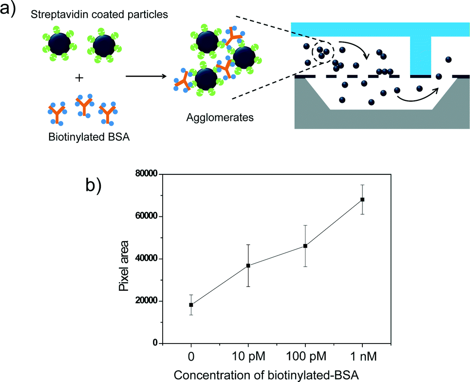
Finally, we applied the Nanoslit-Chip to the detection of biological molecules based on target molecule-induced agglutination of particles. As a proof of concept, we utilized the streptavidin–biotin interaction that is frequently used as a biological model for agglutination assay.35,36 The streptavidin–biotin interaction can induce particle aggregation, which can be trapped and quantified in the Nanoslit-Chip. A particle agglutination-based assay is a relatively simple diagnostic method that has been widely applied to detect viruses, blood groups, and DNA hybridization.35,37–40
In this study, streptavidin-coated fluorescent particles (450 nm) were used as probe nanoparticles, while multi-biotinylated BSA (bovine serum albumin) was mixed with the particles to induce particle aggregation. Fig. 8a illustrates the detection process of the agglutination assay in the Nanoslit-Chip. The multi-biotinylated BSA solution (100 μl) at various concentrations (0 M, 10 pM, 100 pM, and 1 nM, respectively) was incubated with streptavidin-coated fluorescent particles (100 μl, 107 ml−1) for 5 h at 25 °C. The resulting mixture was then diluted to an appropriate concentration that will not give rise to particle-induced clogging (105 ml−1). To reduce non-specific binding of the streptavidin-coated particles to the nanoslit membrane, the Nanoslit-Chip was coated with natural BSA before mixture injection. After that, the diluted mixture was injected into the Nanoslit-Chip at a flow rate of 40 μl min−1 for 10 min and washed using DI water. The target-induced nanoparticle aggregates were trapped on the nanoslit array membrane, while target-unbound single particles passed through the membrane into the bottom fluid channel during the injection and washing steps. The fluorescence pixel areas for the aggregated particles capturing the target protein increase as the concentration of biotinylated BSA increases, as shown in Fig. 8b. This result indicates that the Nanoslit-Chip is able to trap and concentrate the target-bound particle aggregates on nanoslit arrays, which leads to a sensitive detection of the target molecules (ten picomolar concentration). The variations in each measurement of target concentration might result from the multilayer trapping of the agglomerates, non-specific particle aggregation, and particle dilution error. The dynamic range of the agglutination assay based on the Nanoslit-Chip was in the range from 10 pM to 1 nM.
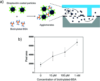 |
| | Fig. 8 a) Schematics of the agglutination assay and the selective trapping of the target-induced nanoparticle aggregates in the Nanoslit-Chip. Biotinylated BSA and streptavidin-coated fluorescent particles (450 nm) are used for the agglutination assay. The aggregates that were induced by the binding of biotinylated BSA (analyte) and the streptavidin-coated fluorescent particles were trapped on the nanoslit membrane. b) Fluorescence signals from the aggregates (pixel area) were shown as a function of the analyte concentration (0, 10 pM, 100 pM and 1 nM, respectively). | |
Conclusion
In this paper, we demonstrate a nanoslit fluidic chip with a nanoslit array membrane (Nanoslit-Chip) for nanoparticle trapping and concentration, as well as its application to the quantitative detection of protein as a model test. The fabrication process of the Nanoslit-Chip and the control of nanoslit sizes are simple and inexpensive due to standard photolithography and the TEOS CVD process. The Nanoslit-Chip containing a large number of nanoslits has several benefits such as low flow resistance and little nanoparticle clogging for separation of nanoparticles. According to our size-dependent trapping principle, large sized particles were easily separated, concentrated, and quantified from the particle mixtures of different sizes in the Nanoslit-Chip. Finally, we applied the Nanoslit-Chip to a sensitive detection of BSA based on target-induced aggregation of nanoparticles. The detection limit was 10 pM, and the dynamic range was 10 pM to 1 nM. The Nanoslit-Chip based size-dependent separation method is expected to be a potential agglutination assay tool for detecting viruses and can be extended to a biomedical device for harvesting desired biomolecules and nanoparticles.
Materials
Normal bovine serum albumin (BSA) and biotinylated-BSA (biotin-BSA) were purchased from Sigma-Aldrich (St. Louis, MO, USA) and used without further purification. Red fluorescent polystyrene particles (1.8 μm) and streptavidin coated blue fluorescent polystyrene particles (SPHERO™ Streptavidin Coated Fluorescent Particles, 450 nm) were purchased from Spherotech (Lake Forest, IL, USA). Deionized (DI) water was used for all experiments.
Acknowledgements
This research was supported by the Pioneer Research Center Program through the National Research Foundation of Korea funded by the Ministry of Science, ICT & Future Planning (NRF-2013-006163).
References
- N. L. Rosi and C. A. Mirkin, Chem. Rev., 2005, 105, 1547–1562 CrossRef CAS PubMed.
- S. G. Penn, L. He and M. J. Natan, Curr. Opin. Chem. Biol., 2003, 7, 609–615 CrossRef CAS PubMed.
- R. A. Álvarez-Puebla and L. M. Liz-Marzán, Small, 2010, 6, 604–610 CrossRef PubMed.
- M. Swierczewska, G. Liu, S. Lee and X. Chen, Chem. Soc. Rev., 2012, 41, 2641–2655 RSC.
- M. Wiklund and H. M. Hertz, Lab Chip, 2006, 6, 1279–1292 RSC.
- Y. H. Tennico, D. Hutanu, M. T. Koesdjojo, C. M. Bartel and V. T. Remcho, Anal. Chem., 2010, 82, 5591–5597 CrossRef CAS PubMed.
- B. H. Jun, M. S. Noh, J. Kim, G. Kim, H. Kang, M. S. Kim, Y. T. Seo, J. Baek, J. H. Kim, J. Park, S. Kim, Y. K. Kim, T. Hyeon, M. H. Cho, D. H. Jeong and Y. S. Lee, Small, 2010, 6, 119–125 CrossRef CAS PubMed.
- H. Chon, S. Lee, S. W. Son, C. H. Oh and J. Choo, Anal. Chem., 2009, 81, 3029–3034 CrossRef CAS PubMed.
- H. Chon, C. Lim, S.-M. Ha, Y. Ahn, E. K. Lee, S.-I. Chang, G. H. Seong and J. Choo, Anal. Chem., 2010, 82, 5290–5295 CrossRef CAS PubMed.
- Y. Liang, J.-L. Gong, Y. Huang, Y. Zheng, J.-H. Jiang, G.-L. Shen and R.-Q. Yu, Talanta, 2007, 72, 443–449 CrossRef CAS PubMed.
- Y. Moser, T. Lehnert and M. Gijs, Lab Chip, 2009, 9, 3261–3267 RSC.
- B.-H. Jun, G. Kim, J. Baek, H. Kang, T. Kim, T. Hyeon, D. H. Jeong and Y.-S. Lee, Phys. Chem. Chem. Phys., 2011, 13, 7298–7303 RSC.
- S. M. Park, Y. S. Huh, H. G. Craighead and D. Erickson, Proc. Natl. Acad. Sci. U. S. A., 2009, 106, 15549–15554 CrossRef CAS PubMed.
- Y. S. Ang and L. Y. L. Yung, ACS Nano, 2012, 6, 8815–8823 CrossRef CAS PubMed.
- M. Wang, N. Jing, I. H. Chou, G. L. Cote and J. Kameoka, Lab Chip, 2007, 7, 630–632 RSC.
- D. Huh, K. L. Mills, X. Y. Zhu, M. A. Burns, M. D. Thouless and S. Takayama, Nat. Mater., 2007, 6, 424–428 CrossRef CAS PubMed.
- I. Choi, Y. S. Huh and D. Erickson, Lab Chip, 2011, 11, 632–638 RSC.
- C. H. Duan, W. Wang and Q. Xie, Biomicrofluidics, 2013, 7, 026501 CrossRef PubMed.
- R. Chantiwas, S. Park, S. A. Soper, B. C. Kim, S. Takayama, V. Sunkara, H. Hwang and Y. K. Cho, Chem. Soc. Rev., 2011, 40, 3677–3702 RSC.
- E. Tamaki, A. Hibara, H. B. Kim, M. Tokeshi and T. Kitamori, J. Chromatogr., A, 2006, 1137, 256–262 CrossRef CAS PubMed.
-
H. Bruus, Theoretical microfluidics, Oxford University Press, Oxford, New York, 2008 Search PubMed.
- R. Yokokawa, Y. Yoshida, S. Takeuchi, T. Kon and H. Fujita, Nanotechnology, 2006, 17, 289–294 CrossRef CAS.
- A. Hibara, T. Saito, H. B. Kim, M. Tokeshi, T. Ooi, M. Nakao and T. Kitamori, Anal. Chem., 2002, 74, 6170–6176 CrossRef CAS.
- T. Yamamoto and T. Fujii, Nanotechnology, 2010, 21, 395502 CrossRef PubMed.
- L. D. Menard and J. M. Ramsey, Nano Lett., 2011, 11, 512–517 CrossRef CAS PubMed.
- X. J. Li, X. D. Wang, J. Jin, Q. S. Tang, Y. C. Tian, S. J. Fu and Z. Cui, Microelectron. Eng., 2010, 87, 722–725 CrossRef CAS PubMed.
- L. H. Thamdrup, A. Klukowska and A. Kristensen, Nanotechnology, 2008, 19, 125301 CrossRef PubMed.
- P. Sivanesan, K. Okamoto, D. English, C. S. Lee and D. L. DeVoe, Anal. Chem., 2005, 77, 2252–2258 CrossRef CAS PubMed.
- A. de la Escosura-Muniz and A. Merkoci, Small, 2011, 7, 675–682 CrossRef CAS PubMed.
- S. M. Wu, F. Wildhaber, O. Vazquez-Mena, A. Bertsch, J. Brugger and P. Renaud, Nanoscale, 2012, 4, 5718–5723 RSC.
- A. M. M. Jani, D. Losic and N. H. Voelcker, Prog. Mater. Sci., 2013, 58, 636–704 CrossRef PubMed.
- T. S. Kustandi, W. W. Loh, H. Gao and H. Y. Low, ACS Nano, 2010, 4, 2561–2568 CrossRef CAS PubMed.
- L. Ceriotti, N. F. de Rooij and E. Verpoorte, Anal. Chem., 2002, 74, 639–647 CrossRef CAS.
- A. Nagy and A. Gaspar, J. Chromatogr., A, 2013, 1304, 251–256 CrossRef CAS PubMed.
- R. Afshar, Y. Moser, T. Lehnert and M. A. M. Gijs, Anal. Chem., 2011, 83, 1022–1029 CrossRef CAS PubMed.
- M. Wiklund, O. Nord, R. Gothall, A. V. Chernyshev, P. A. Nygren and H. M. Hertz, Anal. Biochem., 2005, 338, 90–101 CrossRef CAS PubMed.
- J. Baudry, C. Rouzeau, C. Goubault, C. Robic, L. Cohen-Tannoudji, A. Koenig, E. Bertrand and J. Bibette, Proc. Natl. Acad. Sci. U. S. A., 2006, 103, 16076–16078 CrossRef CAS PubMed.
- J. M. Perez, F. J. Simeone, Y. Saeki, L. Josephson and R. Weissleder, J. Am. Chem. Soc., 2003, 125, 10192–10193 CrossRef CAS PubMed.
- W. Bains, Clin. Chem., 1998, 44, 876–878 CAS.
- S. Vollenhofer-Schrumpf, R. Buresch and M. Schinkinger, J. Microbiol. Methods, 2007, 68, 568–576 CrossRef CAS PubMed.
Footnotes |
| † Electronic supplementary information (ESI) available: Numerical calculations of the hydraulic resistance of Nanoslit-Chip (Fig. S1). SEM images for the nanoslit membrane (Fig. S2). Fluorescence images and the corresponding SEM images for the evaluation of Nanoslit-Chip based quantitative particle analysis (Fig. S3). Trapping the 1.8 μm red fluorescent particles in the nanoslit membrane (Movie S1). See DOI: 10.1039/c3lc50922b |
| ‡ Y. Koh and H. Kang contributed equally to this work. |
|
| This journal is © The Royal Society of Chemistry 2014 |
Click here to see how this site uses Cookies. View our privacy policy here.