Effect of surface morphology changes of Ti-6Al-4V alloy modified by laser treatment on GDOES elemental depth profiles†
Igor S.
Molchan
*a,
Sundar
Marimuthu
b,
Abdeslam
Mhich
a,
Zhu
Liu
a,
Teruo
Hashimoto
a,
George E.
Thompson
a,
David
Whitehead
b,
Zengbo B.
Wang
b,
Paul
Mativenga
b,
Lin
Li
b,
Clive
Grafton-Reed
c,
Ian H.
Leaver
d,
Simon
Cheetham
d and
Steve
Dilworth
d
aCorrosion and Protection Centre, School of Materials, The University of Manchester, The Mill, Sackville St., Manchester, M13 9PL, UK. E-mail: igor.molchan@manchester.ac.uk
bLaser Processing Research Centre, School of Mechanical, Aerospace and Civil Engineering, The University of Manchester, Manchester, M13 9PL, UK
cRolls-Royce plc, PO Box 31, Derby, DE24 8BJ, UK
dBAE Systems (Operations) Limited, Farnborough, Hants GU14 6YU, UK
First published on 2nd November 2012
Abstract
An aerospace grade Ti-6Al-4V alloy, treated by an excimer laser, has been analysed by elemental depth profiling using glow discharge optical emission spectrometry (GDOES). Laser exposure may modify the surface morphology of the alloy due to melting and generation of microcracks. Melting reduces the roughness over an area of 1 × 1 μm, whereas the roughness over an area of 100 × 100 μm increases. The influence of such modification of the surface morphology on changes in the shapes of the GDOES elemental depth profiles is discussed.
Introduction
Glow discharge optical emission spectrometry is a well established technique for elemental depth profile analysis of various solid materials. The use of a radiofrequency source for plasma generation that may operate in both pulsed and continuous modes enables depth profiling of both conducting and non-conducting samples, including metals, semiconductors, glasses and ceramics. Compared with other depth profiling techniques, such as secondary ion mass spectroscopy, Auger electron spectroscopy, time-of-flight secondary ion mass spectroscopy, etc., GDOES operates at a relatively low vacuum of several hundred Pa and is extremely fast due to the high target sputtering rate that may be above 1 μm min−1.1 The potential of GDOES for the analysis of both thick films, of several tens of microns thickness, and thin films, of several nanometres thickness, and multilayered coatings, has been demonstrated.2–5 The high resolution capability of GDOES analysis has been employed in the study of elemental distributions in thin, up to 4 nm thickness, air-formed films on steels and aluminium, and for the study of ionic transport processes during formation of anodic films on aluminium.3,6,7During GDOES examination, material is sputtered over a relatively large surface area, typically 4 mm diameter. This imposes requirements on the quality of the surface. Thus, the ideal surface should be macroscopically flat to fit the sample holder arrangement, and the lower the roughness of the analysed surface, the higher the depth resolution that can be achieved. Increase of surface roughness results in decrease of steepness of the trailing or the leading edges of the elemental profiles, making it difficult to locate precisely the position of interfaces in layered samples and it may even lead to severe degradation of the depth profiles.8,9
Here, the ability of GDOES to analyse thin films and its sensitivity to surface roughness are utilised for analysis of an aerospace grade Ti-6Al-4V alloy that had been subjected to laser exposure. In this communication, the potential of GDOES for examination of laser surface treatment of Ti-6Al-4V and indirect monitoring of surface modification are discussed.
Experimental
Ti-6Al-4V alloy sheet of 1 mm thickness, with a nominal composition (wt%) given as 6 aluminium, 4 vanadium, remainder titanium, cut to dimensions of 25 × 25 mm, was used as a test specimen. The specimens were laser treated in the ambient atmosphere, using a nanosecond-pulsed KrF laser. A 200 mm spherical focusing lens and 10 × 10 mm2 beam shaping mask were used to obtain a 1 × 1 mm2 rectangular laser beam spot over the specimen surface. In order to study the effect of the amount of laser energy transmitted to a specimen on the surface morphology, the laser intensity was varied from 13 to 60 MW cm−2.The surface morphology of the specimens was examined by field emission gun scanning electron microscopy (FEG SEM), using a Zeiss Ultra 55 microscope, equipped with EDX and BSE detectors. A Tecnai 30 transmission electron microscope (TEM), operating at 300 kV, was employed for examination of the air-formed oxide layer on the surface of the alloys. For TEM observation, an electron transparent section of approximately 30 nm thickness was prepared by focussed ion beam milling, using an FEI DualBeam NOVA600i instrument operating at 30 kV. Further, atomic force microscopy (AFM), using a Dimension 3100 microscope (Digital Instruments), operating in the tapping mode, was employed to estimate surface roughness. AFM images were then processed using SPIP software (Image Metrology ApS) to calculate the surface roughness, Sa.
Elemental depth profile analysis was undertaken by GDOES, using a GD-Profiler 2 (Horiba Jobin Yvon) operating in the radiofrequency mode at 13.56 MHz. A 4 mm diameter copper anode and high purity argon gas were used. The optical emissions from the excited sputtered elements were detected with a polychromator of focal length of 500 mm with 30 optical windows. The emission lines used were 396.12 nm for Al, 156.14 nm for C, 121.57 for H, 130.22 nm for O, 365.32 nm for Ti and 411.18 nm for V. Elemental depth profiling was undertaken at an argon pressure of 700 Pa and forward power of 35 W, with a data acquisition time of 0.01 s. Prior to depth profiling, pre-sputtering of a sacrificial monocrystalline silicon wafer was undertaken to clean the GD source.10 As a result, silicon covered the inner surface of the anode, thus minimising contributions from re-sputtering of hydrocarbons adsorbed on the anode and reducing distortion of the depth profile at the commencement of sputtering. The electrical parameters, e.g. plasma impedance, effective power, etc., affecting the sputtering rate, were not monitored in this study since these need the use of special equipment. The sputtering rate in the bulk of the alloy, measured from the crater depth after 3 min of sputtering by a Perthometer S2 (Mahr) surface measuring device, was approximately 2.7 μm min−1.
Results and discussion
Visual observation of the untreated and laser treated alloys reveals relatively rough surface appearances, with the surface of the untreated alloy having a slightly darker appearance. Fig. 1(a) and (b) show GDOES depth profiles of the untreated alloy and the alloy that had been laser treated at 19 MW cm−2. The estimated crater depth achieved for 10 s of sputtering calculated from the sputtering rate is of order of 0.45 μm. The crater depth may be slightly reduced due to plasma instability at the commencement of sputtering. The crater depth may also be affected by non-uniform sputtering due to the surface roughness and the presence of hydrogen on the surface that is discussed further. In general, the depth profiles reveal three regions, comprising (i) a region with increased intensity of oxygen at the commencement of sputtering corresponding to the oxide film on the surface of the alloy, (ii) a transition region where the intensities of the alloy elements, e.g. titanium, aluminium and vanadium, increase gradually and (iii) a steady region where the sputtering front reached the bulk alloy and the signal intensities of the alloy elements remain constant. The GDOES technique is very sensitive to roughness of the surface of the analysed specimen. Roughness is a key factor in limiting the depth resolution of analysis and, for example, if the roughness is similar to the thickness of the analysed layer, severe degradation of depth resolution results.6 Roughness causes non-uniform removal of the material and modification of the surface topography during sputtering.8,11,12 In the depth profiles of materials with rough surfaces, the intensities of the main constituents increase gradually and reach steady values when the surface texture due to roughness is sputtered. A further issue associated with surface roughness is the reduction of the steepness of the trailing and/or leading edges in the profiles of layered materials with increase of roughness. The transition regions in the depth profiles of Fig. 1(a) and (b) have similar durations of about 9–10 s. However, the titanium profiles have different shapes; thus, the titanium signal exhibits a shoulder after the commencement of sputtering, which is followed by an increase of intensity for the laser-treated alloy whereas it increases gradually in the depth profile of the untreated alloy. Successive ultrasonic cleaning in water, ethanol and acetone (15 min duration for each individual step) changed significantly the depth profile of the untreated alloy. The transition region width is reduced significantly to about 1.5 s (Fig. 1(c)).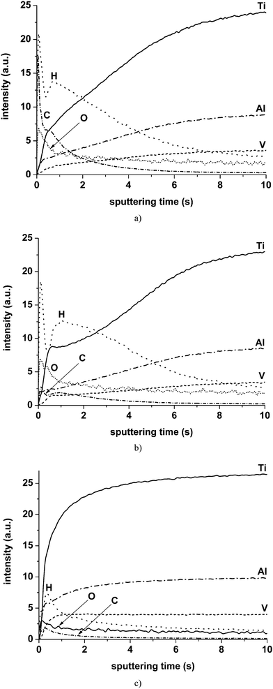 | ||
| Fig. 1 GDOES elemental depth profiles: (a) as-received untreated alloy; (b) alloy laser treated at 19 MW cm−2; (c) as (a) after ultrasonic cleaning consequently in water, ethanol and acetone. | ||
The depth profile of the untreated alloy exhibits an intense carbon peak, originating mostly from hydrocarbons adsorbed on the surface of the alloy. Other carbon-related contaminants, e.g. free carbon, oil, grease, etc., may also be present on the surface. The intensity of the carbon signal reduces after laser exposure mainly due to removal of the hydrocarbons. Examination of the as-received untreated alloy by SEM reveals numerous darker hydrocarbon-related regions on the surface that are absent after laser treatment. Application of ultrasonic cleaning to the as-received untreated alloy leads to a greater reduction of the intensity of carbon signal compared with laser treated alloy. The integrated intensity of the carbon signal for the untreated alloy, calculated over the region of 0–5 s of sputtering time, is about 2.5 and 5 times greater than that for the laser treated alloy and ultrasonically cleaned alloy respectively.
The behaviour of the hydrogen profiles is generally similar to the carbon profiles. The carbon and hydrogen signals show sharp peaks at the commencement of sputtering for the untreated alloy and the alloy treated at 19 MW cm−2 followed by less intense and broader peaks (Fig. 1(a) and (b)). In the depth profile of the ultrasonically cleaned alloy of Fig. 1(c), only single hydrogen and carbon peak, centred at the same location on the sputtering time axis, are evident. The intensities of hydrogen peaks after application of laser treatment are slightly reduced. After ultrasonic cleaning, the intensity of the hydrogen peak reduces by approximately two times compared with that of the untreated alloy. Additional study is required to explain the nearly the same intensities of the hydrogen peaks for the as-received untreated and laser treated alloys. Probably, laser treatment does not remove efficiently other hydrogen-related species, e.g. water. Application of cleaning by low-energy plasma of the GD-source10 at a power of 3 W, pressure of 600 Pa for 600 s to the as-received untreated alloy prior to sputtering resulted in an approximately 3.9-fold reduction of the integrated intensity of the carbon peak. The shape and intensity of the hydrogen signal remained similar to those after laser treatment (see ESI 1†).
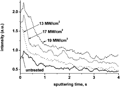
Thus, the extended transition region in the depth profile of the untreated alloy before cleaning compared with that after cleaning is caused mainly by the presence of hydrocarbon contamination. Fernandez et al.14 reported that addition of small amounts of hydrogen to argon may significantly affect the plasma behaviour, leading to a change of sputtering rate and, consequently, an increase or decrease of the signal intensities depending on the element. Conversely, the presence of small amounts of hydrogen in the analysed specimen may also distort the depth profile. For example, analyses of anodic films formed on tantalum and aluminium substrates, but with dissolved hydrogen beneath the oxide–metal interface, revealed marked decreases of the intensities in the tantalum or aluminium signals near the anodic film–metal interface regions that coincided with the relatively intense hydrogen peak.7,15 In order to study the origin of the relatively large width of the transition region in the depth profiles of the laser-treated alloy compared with the cleaned untreated alloy, laser treatment was undertaken with various laser energies transmitted to the specimen by varying the angle of incidence of the laser beam. Fig. 2 compares the titanium and hydrogen profiles of the alloys treated at 13, 17 and 19 MW cm−2 and the ultrasonically cleaned untreated alloy. An increase of the transition region width in the titanium signal is evident for all the laser-treated alloys compared with the ultrasonically cleaned untreated alloy. Further, the width of the transition region increases with increase of the incidence angle of the laser beam. The titanium signal intensity increases rapidly within about 1 s of sputtering for the cleaned untreated alloy, whereas this time increases to approximately 3, 6 and 7 s for the alloys treated at 13, 17 and 19 MW cm−2 respectively. Furthermore, the shoulder in the titanium profile is present for the laser treated alloys, with the width increasing from approximately 0.2 to 1 s with increase of incidence angle. Hydrogen signals of the laser treated alloys exhibit sharp peaks at the commencement of sputtering followed by the extended second peaks. The widths of the second peaks correlate well with the width of the transition region in the titanium profile.
 | ||
| Fig. 2 GDOES titanium and hydrogen depth profiles of the ultrasonically cleaned untreated alloy and alloys laser treated at various intensities (the laser intensity is designated by corresponding numbers; u – untreated alloy). | ||
Fig. 3 displays scanning electron micrographs of the ultrasonically cleaned untreated alloy and the alloy treated at 19 MW cm−2. Relatively bright, sharp-edged features on the surface correspond to the beta-phase of increased vanadium contents of up to 12 at.%, according to local EDX analysis. The remaining surface represents the alpha-phase, with vanadium contents that do not exceed 2–3 at.%. Individual grains of nearly micron dimensions, separated by sharp boundaries, are evident within the beta-phase areas. Laser treatment leads to significant modification of the surface texture due to melting. The sharp edges of the beta-phase areas are transformed to smoother boundaries that separate individual grains in the alpha-phase areas. Scrutiny of the surface of the treated alloy enables observation of shallow, parallel grooves and microcracks with lengths of less than 1 micron. SEM examination of the surface of the alloys treated at 13 and 17 MW cm−2 revealed reduction in the degree of melting that was evident from the decrease of surface smoothing with decrease of laser fluence compared with that treated at 19 MW cm−2.
 | ||
| Fig. 3 Scanning electron micrographs of the surface of (a) ultrasonically cleaned untreated alloy and (b) alloy laser treated at 19 MW cm−2. | ||
As previously mentioned, surface roughness results in a more gradual increase of the signal during GDOES elemental depth profiling, revealing more extended transition regions in the depth profile. However, a smoother surface according to SEM observation also causes a more extended transition region in the GDOES depth profile. Molitor and Young13 reported that laser treatment of a Ti-15-3 alloy reduces microroughness due to general smoothing of the surface by melting, as observed by SEM at a magnification of 5000×. Conversely, macroroughness on the 10 μm scale was increased due to generation of craters by ablation. Table 1 records the surface roughness determined by AFM for the cleaned untreated alloy and the alloy treated at 19 MW cm−2. Scanning has been undertaken over three areas of different dimensions, namely 1 × 1, 20 × 20 and 100 × 100 μm. After laser irradiation, the surface roughness, Sa, decreases, remains without significant change and increases within the 1 × 1, 20 × 20 and 100 × 100 μm areas respectively. Thus, an increase of roughness over a relatively large surface area may contribute to the increase of the width of the transition region in the GDOES depth profiles, even though the roughness over a relatively small area decreases. It should be noted that relatively high hydrogen peaks may contribute to the widths of the transition regions.
| Area, μm2 | |||
|---|---|---|---|
| 1 × 1 | 20 × 20 | 100 × 100 | |
| Untreated | 10.5 | 97 | 214 |
| Laser treated | 3.8 | 98 | 270 |
Further, Fig. 4 compares the oxygen profiles of the laser treated and ultrasonically cleaned untreated alloys. In most of the GDOES depth profiles, the oxygen signal is noisy and, hence, it was smoothed using the averaging tool in the Origin software. The intensity of oxygen peak reduces with the angle of incidence of the laser beam and is of minimum intensity for the untreated alloy. The width of the region from the commencement of sputtering to the trailing edge of the oxygen peak, i.e. the point where the rapid decrease of the oxygen signal intensity is terminated, varied from approximately 0.3 s for the alloy laser treated at 13 MW cm−2 to 0.9 s for that treated at 19 MW cm−2.
 | ||
| Fig. 4 GDOES oxygen depth profiles of the ultrasonically cleaned untreated alloy and the alloys laser treated at various intensities. | ||
Additionally, the peaks are followed by extended tails where the oxygen signal reduced slowly. The intensities of the tails increase in the following order: ultrasonically cleaned untreated alloy < alloy treated at 13 MW cm−2 < alloy treated at 17 MW cm−2 < alloy treated at 19 MW cm−2. It is unlikely that exposure to the short-pulse laser under the selected conditions leads to significant thickening of the air-formed oxide layer on the surface of the alloy that is of several nanometres thickness. Anodic oxidation of the laser-treated and untreated alloy in 0.1 M ammonium pentaborate at a constant current density of 5 mA cm−2 has been undertaken to estimate the difference between oxide film thicknesses. In the selected electrolyte at a constant current density, a barrier type anodic film is formed on the surface of aluminium and titanium. The film thickness depends on the voltage at which film growth is terminated and can be precisely determined from the formation ratios of the anodic films on the respective metals.16,17 Formation of anodic films commences after the initial voltage surge in the voltage–time response; from the height of surge, the thickness of oxide film covering the macroscopic metal surface may be precisely determined from the expected formation ratio. The voltage–time responses recorded during anodising of the laser treated and the untreated alloys (Fig. 5) do not reveal marked differences in the initial surges that are about 3 V; this is indicative of approximately similar thicknesses of the oxide films on both alloys. Given the formation ratio of anodic film on titanium of about 2 nm V−1,17 the oxide film thickness is estimated to be about 6 nm.
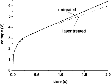 | ||
| Fig. 5 Voltage–time responses recorded during anodising of the untreated alloy and alloy after laser treatment at 19 MW cm−2 in 0.1 M ammonium pentaborate at a constant current density of 5 mA cm−2. | ||
TEM-examination of the near surface region of the laser treated and untreated alloys confirms the data obtained by anodising, revealing an air-formed oxide layer of 6 nm thickness for the untreated alloy and the alloy treated at a relatively high laser intensity of 60 MW cm−2 (Fig. 6). This suggests that the observed trends in titanium and oxygen profiles of Fig. 2 and 4 respectively are caused by consumption of metallic asperities due to the surface roughness covered by a thin oxide layer. Additionally, microcracks generated on the surface of laser treated alloy may contribute to formation of the shoulder and extend the transition region in the GDOES profile.
 | ||
| Fig. 6 Transmission electron micrographs of cross-sectional views of near surface region of (a) untreated alloy and (b) alloy laser treated at 60 MW cm−2. | ||
Conclusions
The potential of GDOES for the study of the effect of laser exposure on an aerospace Ti-6Al-4V alloy has been demonstrated. It is shown that GDOES may effectively provide indirect, comparative information about changes of surface texture. Treatment of the surface of the Ti-6Al-4V alloy by the excimer laser reduces the amount of hydrocarbon contaminants. Consequently, the surface of the alloy is modified by elevated temperature exposure under laser treatment, resulting in smoothing of the surface due to melting and development of microcracks. In spite of the smoother surface appearance of the laser treated surface observed by SEM, the macroscopic surface roughness is increased. It is suggested that the increase of macroscopic roughness and generation of microcracks over the laser treated surface lead to distortion of the GDOES depth profile. This appears as an extension of the transition region, i.e. the region from the commencement of sputtering, with a gradual increase of the alloying element intensity signals, to the steady region. In summary, GDOES depth profile analysis is very fast; it takes a few minutes, with most time spent for cleaning of the GD source by pre-sputtering of the sacrificial specimen, whereas analysis of the alloys is completed within 10–15 s. Thus, the technique may be easily adopted for control of contaminants and estimation of the extent of surface changes in industrial processes utilised for preparation of alloy surface for bonding involving laser treatment. Further, when GDOES results are combined with information from other analytical techniques, e.g. SEM, TEM, etc., the outcome is important for understanding of fundamental processes of interaction of laser beam with metals and alloys.Acknowledgements
This work has been undertaken under SAMULET Project. Support of the Engineering and Physical Sciences Research Council (UK) and Technology Strategy Board (UK) is acknowledged.References
- R. Payling, Spectroscopy, 1998, 13, 36–43 CAS.
- B. Fernandez, N. Bordel, R. Pereiro and A. Sanz-Medel, J. Anal. At. Spectrom., 1997, 12, 1209–1214 RSC.
- K. Shimizu, H. Habazaki, P. Skeldon, G. E. Thompson and G. C. Wood, Surf. Interface Anal., 2000, 29, 743–746 CrossRef CAS.
- T. K. Rout, Scr. Mater., 2007, 56, 573–576 CrossRef CAS.
- U. Becka, G. Reinersa, Th. Wirtha, V. Hoffmannb and F. Präßler, Thin Solid Films, 1996, 290-291, 57–62 CrossRef.
- K. Shimizu, H. Habazaki, P. Skeldon, G. E. Thompson and G. C. Wood, Surf. Interface Anal., 1999, 27, 998–1002 CrossRef CAS.
- K. Shimizu, G. M. Brown, H. Habazaki, K. Kobayashi, P. Skeldon, G. E. Thompson and G. C. Wood, Electrochim. Acta, 1999, 44, 2297–2306 CrossRef CAS.
- K. Shimizu, G. M. Brown, H. Habazaki, K. Kobayashi, P. Skeldon, G. E. Thompson and G. C. Wood, Surf. Interface Anal., 1999, 27, 153–156 CrossRef CAS.
- N. Trigoulet, T. Hashimoto, I. S. Molchan, P. Skeldon, G. E. Thompson, A. Tempez and P. Chapon, Surf. Interface Anal., 2010, 42, 328–333 CrossRef CAS.
- I. S. Molchan, G. E. Thompson, P. Skeldon, N. Trigoulet, P. Chapon, A. Tempez, J. Malherbe, L. Lobo Revilla, N. Bordel, Ph. Belenguer, T. Nelis, A. Zahri, L. Therese, Ph. Guillot, M. Ganciu, J. Michler and M. Hohl, J. Anal. At. Spectrom., 2009, 24, 734–741 RSC.
- N. Trigoulet, N. Tuccitto, I. Delfanti, A. Licciardello, I. S. Molchan, P. Skeldon, G. E. Thompson, A. Tempez and P. Chapon, Surf. Interface Anal., 2011, 43, 183–186 CrossRef CAS.
- J. Malherbe, H. Martinez, B. Fernández and O. F. Donard, Anal. Bioanal. Chem., 2010, 396, 2841–2853 CrossRef CAS.
- P. Molitor and T. Young, Int. J. Adhes. Adhes., 2004, 24, 127–134 CrossRef CAS.
- B. Fernandez, N. Bordel, R. Pereiro and A. Sanz-Medel, J. Anal. At. Spectrom., 2003, 18, 151–156 RSC.
- A. Tempez, S. Canulescu, I. S. Molchan, M. Döbeli, J. A. Whitby, L. Lobo, J. Michler, G. E. Thompson, N. Bordel, P. Chapon, P. Skeldon, I. Delfanti, N. Tuccitto and A. Licciardello, Surf. Interface Anal., 2009, 41, 966–973 CrossRef CAS.
- L. Young, Anodic Oxide Films, Academic Press, New York, 1960 Search PubMed.
- A. Aladjem, J. Mater. Sci., 1973, 8, 688–704 CrossRef CAS.
Footnote |
| † Electronic supplementary information (ESI) available. See DOI: 10.1039/c2ja30186e |
| This journal is © The Royal Society of Chemistry 2013 |