 Open Access Article
 This Open Access Article is licensed under a
 Creative Commons Attribution 3.0 Unported Licence
A systematic study of the influence of nanoelectrode dimensions on electrode performance and the implications for electroanalysis and sensing
Ilka Schmueserab,
Anthony J. Waltonb,
Jonathan G. Terryb,
Helena L. Woodvinea,
Neville J. Freemancd and
Andrew R. Mount*a
aEaStCHEM, School of Chemistry, The University of Edinburgh, King's Buildings, Edinburgh, EH9 3JJ, UK. E-mail: A.Mount@ed.ac.uk
bSchool of Engineering, The University of Edinburgh, King's Buildings, Edinburgh, EH9 3JF, UK
cSchool of Physics & Astronomy, Manchester University, Oxford Road, Manchester M13 9PL, UK
dNanoFlex Ltd, Daresbury Innovation Centre, Keckwick Lane, Daresbury, WA4 4FS, UK
First published on 20th August 2013
Abstract
Micron resolution photolithography has been employed to make microsquare nanoband edge electrode (MNEE) arrays with reproducible and systematic control of the crucial dimensional parameters, including array element size and spacing and nanoelectrode thickness. The response of these arrays, which can be reproducibly fabricated on a commercial scale, is first established. The resulting characteristics (including high signal and signal-to-noise, low limit of detection, insensitivity to external convection and fast, steady-state, reproducible and quantitative response) make such nanoband electrode arrays of real interest as enhanced electroanalytical devices. In particular, the nanoelectrode response is presented and analysed as a function of nanometre scale electrode dimension, to assess the impact and relative contributions of previously postulated nanodimensional effects on the resulting response. This work suggests a significant contribution of migration at the band edges to mass transfer, which affects the resulting electroanalytical response even at ionic strengths as large as 0.7 mol dm−3 and for electrodes as wide as 50 nm. For 5 nm nanobands, additional nanoeffects, which are thought to arise from the fact that the size of the redox species is comparable to the band width, are also observed to attenuate the observed current. The fundamental insight this gives into electrode performance is discussed along with the consequent impact on using such electrodes of nanometre dimension.
1. Introduction
There has been considerable interest in the fabrication and deployment of miniaturized electrodes for over twenty years. The potential benefits of these electrodes have been widely discussed in the literature.1–7 The enhanced mass transport due to the hemispherical or radial diffusion that occurs on the micron scale gives high current densities and steady-state or near steady-state currents, reducing the effects of convection. Additionally, shorter RC time constants allow the investigation of faster electrode processes, while smaller iR drops enable the electrodes to work in a wide range of resistive electrolytes, with little or no added ions. As these effects are enhanced with decreasing electrode size, there has been considerable recent interest in scaling electrodes from the micron8 to the nanoscale.9–20 Such electrode structures also offer the opportunity to exploit nanostructural effects such as enhanced surface catalytic activity,21–23 and nanoelectrode systems have been constructed for applications as diverse as enhanced thermal energy24 and light harvesting.25,26 However, there are two main issues with current nanoelectrode technology. The first is the lack of a suitable technology for reproducibly manufacturing electrodes with accurately controlled dimensions at a reasonable cost and volume to enable commercialisation. The second is the low current levels measured with nanoelectrodes (often in the pA range),15,27 which require precision low current, low noise potentiostats, with efficient electromagnetic shielding. These are the issues addressed by this work.One way by which this latter issue can be addressed is by multiplying the observed current through the simultaneous measurement of large numbers of arrayed nanoelectrodes.9,12 The simplest methods involve no specific control over the inter-electrode spacing of array devices, which are often referred to as ensembles.12 A range of fabrication techniques have been adopted to produce ensemble devices, typically employing either a method to open pores in insulating layers deposited over conductive materials, thereby exposing an ensemble of active electrode areas (e.g. ultrasound28 or neutron track etching29), templated growth in the nanopores of membranes30,31 or the imprinting of structures.32 This is at present an area of considerable research interest,33 but the challenge with ensemble technologies is that it is currently not possible to produce large nanoelectrode arrays with systematic control of the size and separation of each electrode. Without this, there is heterogeneity of individual electrode response, with individual electrodes being affected by diffusional layer overlap from neighbouring electrodes to variable extents as a function of time and frequency. The average spacing is also often hard to control and optimise.
The alternative is to produce ordered nanoscale arrays. Some ensemble methods (X-rays34 and structure imprinting) show potential for control of spacing, (indeed recent work has demonstrated production of nanopore arrays with embedded ring electrodes in each pore35) but these involve considerable expense and/or complexity. Conventional photolithography, such as is used in the semiconductor industry, typically requires wafer stepper based technology, which is clearly capable of delivering well-controlled and reproducible nanoarrays. However, the cost of ownership of a modern state-of-the-art, nanometre capable wafer stepper is extremely high. Another option is e-beam lithography.36 However, this suffers from being an essentially serial writing process and hence is both time consuming and costly. Nano imprint lithography37 potentially addresses the throughput issue, but has the high cost of producing the nanoscale mask required for making the mould. As a result of the expense and complication of the above approaches most of the nanoelectrodes reported have employed alternative design and production strategies.
It is also possible to use lower cost, micron resolution photolithography and reactive ion etch techniques to fabricate arrays of individually addressable submicron band electrodes, (e.g. 2 mm long with widths as small as 37 nm38,39). Similarly, groups have used (optical) lithographically patterned nanowire electrodeposition (LPNE) to prepare a sacrificial nickel nanoband electrode, which acts as a seed layer for the subsequent electrodeposition of a noble metal. The nickel electrode is recessed in a trench, such that the electrodeposition forms a nanowire of rectangular cross-section, after subsequent removal of the sacrificial layers. This results in closely spaced, millimetre long gold nanowires in the form of bands and grids.40,41 Both of the above process architectures produce long nanobands or nanowires with significant resistance, which are ideally suited for applications such as resistive gas sensing.42 However, long nanowires/bands are potentially susceptible to line breakages occurring during the fabrication process and/or operation, and as with all band electrodes, their mass transport limited electroanalytical response is not steady-state.
In addition to photolithographic methods, other approaches have been reported for patterning arrays43 to give electrode elements arranged in an ordered manner with well-defined inter-electrode spacing, including controlled polymer deposition, orientation and selective dissolution,44 as well as carbon nanotube (CNT)45,46 and boron-doped diamond47 nanowire assemblage. However, the challenge with polymer deposition is to control the electrode size and spacing, while CNT assemblies still require standard lithographic patterning (e.g. e-beam) of nanoscale metal catalyst centres and the nanotubes themselves are not uniform in length, diameter or orientation. In essence, the above methods all require extremely precise nanopatterning procedures and lack flexibility and control of both the electrode material and its size. A final fabrication approach that has been reported is nanoskiving,48,49 which when producing arrays, requires addressing the challenges of first sectioning materials encapsulating nanowires, and then collecting, mounting and connecting them on a suitable support.
This paper utilizes our own nanoelectrode array design;50 the microsquare nanoband edge electrode (MNEE, Fig. 1), which has been developed to address some of these issues and is fabricated using reliable, readily available and well characterized standard micron scale microfabrication techniques. The precise fabrication process developments required to produce these systems are detailed elsewhere,51 as is the 1000 fold increase in detection sensitivity observed at an MNEE system compared to a single microelectrode of comparable electrode area.52 In this work, the fundamental response of these systems is first considered to demonstrate that the resulting response is both quantifiable and reproducible as well as displaying the characteristics of a nanoscale electrode system of high effective area. These systems are then used to first measure and then consider the impact of nanoscale effects previously postulated and reported as occurring at other nanoelectrode systems.
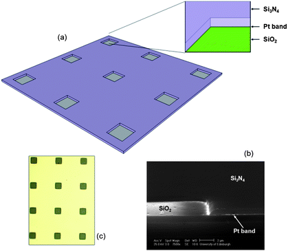 | ||
| Fig. 1 (a) Schematic diagram of the microsquare nanoband edge electrode (MNEE) array architecture used in this work, with Si3N4 upper (purple) and SiO2 lower (green) insulation sandwiching a Pt nanoband (grey) in each square aperture (inset). (b) an SEM image of a cleaved and polished cross section through a square aperture in the fabricated 10μ3D50n structure. The horizontal line of enhanced scattering indicating the 50 nm Pt band is highlighted, which as expected is seen to extend around the perimeter of the half aperture with SiO2 at its base in the left of the picture. (c) an optical microscope image of the fabricated microsquare array. | ||
2. The MNEE system
Fig. 1 shows the details of the electrode architecture, which was produced on 3-inch n-type silicon wafers using contact/proximity based photolithography, together with an SEM showing a section through one element of the array device. The square aperture edge dimension, separation between apertures and nanoband thickness has been systematically varied and is denoted by the nomenclature LμHDMn, where L is the edge dimension, in microns, H is the closest interaperture spacing ratioed to the edge dimension and M is the nanoband thickness. For example, exemplar characterisation has been carried out on a system with these dimensions set at 10 μm, 30 μm and 50 nm, denoted 10μ3D50n. The depth of the square aperture etched to expose the nanoband was controlled to ensure that the nanoband was located at the base of the etched hole.3. Experimental
Electrochemical measurements were carried out in a Faraday cage using Autolab PGSTAT30 or PGSTAT128N potentiostats controlled via a PC and a frequency response analyser module (Windsor Scientific). General Purpose Electrochemical Software (GPES, version 4.9), Frequency Response Analysis (FRA, version 4.9) and NOVA (version 1.9) were used for data collection of cyclic voltammetry and electrochemical impedance spectroscopy (EIS) measurements. The fabricated nanoelectrode arrays were used as working electrodes, with a saturated calomel reference electrode and a platinum gauze counter electrode. All potentials, E, are quoted with respect to this reference electrode. Prior to experimentation, the glassware was rinsed in sulphuric acid (Chestech, 96% purity) to remove any organic contamination.All solutions were prepared using deionized water (Millipore MilliQ). Aqueous 0.5 M potassium chloride (Fisher Scientific, 99.6% purity) solution was used for electrochemical cleaning. Redox measurements used 100 μM ferrocene carboxylic acid (FCA, Alfa Aesar, 98% purity) in either 0.1 M potassium chloride background electrolyte in a solution (pH = 7.0) prepared with 0.1 M citric acid (Fisher Scientific, 100.3% purity) and 0.3 M sodium hydroxide (Fisher Scientific, 97% purity), effectively 0.1 M trisodium citrate solution (FCA(I) solution) or the same concentration of FCA in a ten times diluted electrolyte solution (pH = 7.0) of 10 mM potassium chloride, 10 mM citric acid and 30 mM sodium hydroxide (FCA(I/10) solution). Hexaammineruthenium(III) (HAR) chloride (Aldrich, 98% purity) measurements were recorded at 100 μM concentration in 0.5 M (HAR(I) solution) and 10 mM (HAR(I/50) solution) potassium chloride electrolyte solutions that were deoxygenated using argon.
4. MNEE characterisation
4.1 COMSOL FE validation and modelling
Various methods for the modelling of diffusion limited chronoamperometric currents have been reported based on commercial53 and in-house software.54,55,56 They involve solving Fick's second law for the considered geometry using different explicit, implicit and semi-implicit techniques to solve the resulting matrices.The advantages of using commercial finite element modelling (FEM) software packages such as COMSOL include their ready availability and their relatively large user base, which has led to the validation of the resultant modelling with experimental measurement for a wide variety of applications. However, concerns have been raised about the validity of this approach for transient microdisc, microhemisphere and microband 3D simulations,57,58 which has led to the development and assessment of the validity of other finite difference, finite element, finite volume and other modelling methods, many of which are not routinely available in COMSOL. These models have been reviewed in the context of their correspondence to microelectrode voltammetric theory.59 This highlights the need for prior benchmarking and validation of any FEM modelling employed on a comparable system with known analytical response. In our previous steady-state COMSOL FEM simulations of single microsquare response,53 we therefore first successfully benchmarked our modelling to the analytical response of a microdisc of similar dimension. In this work we extend this approach, first benchmarking the time-dependent response at steady-state to that obtained from a time-dependent COMSOL microdisc simulation.
Time-dependent three-dimensional FE simulations of the simulation cube were carried out using COMSOL 3.5a for Linux (COMSOL, Inc., Burlington, Massachusetts, USA). Although it is clear that microdisc simulation could have been reduced to a two dimensional problem by using rotational symmetry, this option was not chosen to keep the microsquare, microdisc and MNEE simulations as similar as possible for benchmarking. (However, taking advantage of the symmetry about the plane (x = y) in the simulation cube, Fig. 2, only half the cube was required to be modelled). Previous experiments and 2D simulations on microdisc array electrodes have established negligible diffusion layer overlap between neighbouring array elements at steady-state when electrodes are separated by more than 24 times the disc radius,60,61 which indicates steady-state diffusion is established when the diffusion layer thickness is of the order of 12 times the radius. Previous microsquare simulation also showed no boundary effects with the cube dimension set at 20 times the edge length.53 The simulation cube edge length in this work was therefore set at 100 times the microdisc radius or 50 times the edge length, as appropriate, to ensure no boundary edge effects. The concentration at the upper face of the simulation cube and throughout at time zero was then fixed at the bulk concentration of the redox species.
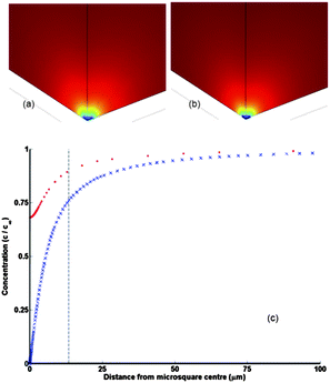 | ||
| Fig. 2 Concentration profiles at the onset of a steady state current for (a) a quarter of a microsquare (edge length, L = 10 μm) and (b) a quarter of an MNEE (L = 10 μm, thickness 50 nm) placed in the near corner of the bottom face (the x, y, 0 plane) of the simulation cube and simulated using FE modelling. In this simulation the diffusion coefficient was set to 10−6 cm2 s−1, and the colours span a concentration range of c = 0 (blue) to c = c∞ = 1 mM (red). (c) the concentration along the z axis normal to the microsquare centre for the microsquare (blue crosses) and the MNEE (red dots); values are normalized to the bulk concentration c0. The concentration at the microsquare centre is not zero for the MNEE electrode as this is an insulator rather than an electroactive surface. The vertical line is the hemispherical radius within which complete redox conversion of FCA occurs, calculated from the volume, V, determined from CNmax and eqn (7). | ||
The user-defined mesh was first optimised in a parametric study to find the combination of number of nodes and node distribution (linear, one- or two-sided logarithmic) for each boundary and volume that showed a converged current response. Subdomains were used to facilitate this process. The final mesh density reflected the reagent concentration gradient within each mesh box, which as expected decreased dramatically as a function of distance from the electrode surface. A parametric study was then used to analyse the various settings COMSOL offers for the solution of the matrix. This revealed very little effect on the modelling results but large variations in efficiency. After pretreatment with the Algebraic Multigrid (hierarchy quality 3) preconditioner, the system was solved using the Conjugate Gradients solver. The required tolerance levels for a converged response were determined as 0.01 (relative tolerance) and 0.001 (absolute tolerance).
Microdiscs of radius, r = 5, 10, 15 and 25 μm were simulated by stepping the redox ion concentration at the electrode boundary to zero at time zero, using 235![[thin space (1/6-em)]](https://www.rsc.org/images/entities/char_2009.gif) 000, 348000, 577000 and 572000 degrees of freedom, respectively. Values were obtained at times between 10−7 s and 105 s and from these the normal diffusive flux at the electrode surface was calculated. Integration of this flux over the electrode area, then multiplication by Faraday's constant, gave the electrode redox current. After about twenty seconds the current was observed to be constant to within 0.1% with time for all microdiscs, indicative of a steady-state current; these relatively small variations were considered to arise from rounding errors. The mean value of the current recorded after this time was reported as the steady-state current.
000, 348000, 577000 and 572000 degrees of freedom, respectively. Values were obtained at times between 10−7 s and 105 s and from these the normal diffusive flux at the electrode surface was calculated. Integration of this flux over the electrode area, then multiplication by Faraday's constant, gave the electrode redox current. After about twenty seconds the current was observed to be constant to within 0.1% with time for all microdiscs, indicative of a steady-state current; these relatively small variations were considered to arise from rounding errors. The mean value of the current recorded after this time was reported as the steady-state current.
This steady-state current was then validated against the limiting current given by:
| iL = BNnFDc∞L | (1) |
485 C mol−1), N is the number of electrodes in the array, n is the number of electrons transferred in the redox reaction and B is a constant depending on microelectrode geometry. For a single disc this means B = 4, N = 1 and L = r.1,62,63 The difference between modelling and simulation values at steady-state was found to be 0.2% for the smallest r, rising to 3% for the largest. This indicates that we can determine steady-state currents for microsquare and MNEE electrodes of similar dimension using COMSOL transient FE modelling to an accuracy of the order of 1% using this approach.
Previous COMSOL FE steady-state simulation and experimental measurement53 also showed that for an edge length, L = 50 μm single microsquare electrode system, the steady-state diffusion limited current, iL, is larger than the microdisc of equivalent area, and given by eqn (1) with a value of B = 2.34.53
Time-dependent modelling of both the L = 10 μm microsquare and the L = 10 μm 50 nm thick single MNEE was then carried out using the approach described above. For the microsquare, the resulting mesh consisted of 195000 degrees of freedom; whilst the MNEE mesh was made slightly denser particularly close to the electrode edges and at the top edge of the aperture, resulting in 352000 degrees of freedom. This gave steady-state mass transport limited currents of 226 pA for a microsquare electrode and 92 pA for the MNEE (for a bulk concentration of redox species of 10−3 mol dm−3 and a diffusion coefficient of 10−6 cm2 s−1).
It is reassuring that the simulated single microsquare steady-state current is consistent with eqn (1), with B = 2.34, which provides further validation of this approach. It is also interesting that both the microsquare and MNEE current values are comparable (with B = 0.956 for MNEE, 41% of that for the microsquare). This indicates that the predominance of the contribution of edge diffusion to the limiting current in microsquares is such that the MNEE produces a comparable mass transport limiting current, with only 2% of the effective electrode area. This modelling also showed that, consistent with previous simulation,53 placing the microsquare or MNEE at the bottom of the shallow aperture had little effect on the limiting current obtained. The calculated concentration profiles (Fig. 2) also indicate that the closed geometry of the MNEE produces hemispherical diffusion layers which is consistent with time-independent mass transport limited diffusion. It is advantageous and not unexpected that the MNEE response is more similar to a microsquare electrode response than to a semi-infinite linear band, for which pseudo steady-state conditions only are observed,38,39,64–66 as similar behaviour has been previously observed and modelled for other closed systems e.g. microsquare, microdisc53 and microring67 electrodes.
4.2 Experimental MNEE characterisation
Experimental MNEE voltammetry (Fig. 3a) shows a near sigmoidal response at v = 100 mV s−1 characteristic of the steady-state response expected from a nanoarray with N = 15625 independent electrodes. However, even at this sweep rate, a significant current can be observed (Fig. 3b) from parasitic capacitance, which arises from non-Faradaic charging (of the capacitance between the platinum plane and solution through the nitride and oxide insulator and silicon substrate, see Fig. 4a). The insensitivity of this additional CV current to potential is consistent with this non-Faradaic capacitance, which as expected linearly increases with v, which explains its growing importance at increasing sweep rates.
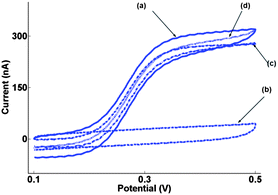 | ||
| Fig. 3 (a) Typical MNEE array first sweep CV at v = 100 mV s−1 for the oxidation of 0.1 mM FCA in aqueous pH = 7.0 solution (0.1 M citric acid/0.3 M sodium hydroxide with 0.1 M potassium chloride; background electrolyte); and for (b) background electrolyte alone. (c) The difference between (a) and (b). (d) The mean of forward and backward scans of (a). The onset potential was 100 mV with the initial direction of scan to positive potentials. | ||
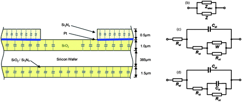 | ||
| Fig. 4 (a) The origin of the parasitic capacitance associated with the MNEE array. (b) Equivalent circuit which describes the parasitic capacitance in parallel with the MNEE array response. (c) Established modified Randles equivalent circuit appropriate for a microsquare electrode array. (d) Equivalent circuit used for the MNEE array. | ||
As this charging current is in parallel with the redox current, subtraction of the response without redox agent at any sweep rate leads to the MNEE array redox response (Fig. 5). In fact, the near constant non-Faradaic capacitance means that at fast sweep rates, when there is time-independent sigmoidal redox response, simple averaging at each potential of the data from forward and backward voltammetric scans essentially leads to this redox response (Fig. 3d). It is reassuring that comparing experiment and modelling results in a sensible value of D = 2.2 × 10⁻⁶ cm2 s−1 being obtained from eqn (1).
 | ||
| Fig. 5 Typical subtracted first sweep CVs (as in Fig. 3c) of the 10μ3D50n MNEE array for the oxidation of 0.10 mM ferrocene carboxylate (FCA solution) at v = (a) 5 V s−1, (b) 1 V s−1, (c) 500 mV s−1, (d) 100 mV s−1, (e) 50 mV s−1, (f) 10 mV s−1, (g) 5 mV s−1, (h) 1 mV s−1. The onset sweep potential was 100 mV with the initial direction of scan to positive potentials. | ||
However, at slower sweep rates, there is an increasing overlap of the growing hemispherical diffusion layers from neighbouring microsquares.66 This causes a decrease in the redox current with time (and decreasing sweep rate) in the subtracted voltammograms (Fig. 5), where the time-independence of the redox response is lost and simple averaging cannot be employed.
The MNEE impedance response, as with the voltammetric data, also shows the backplane non-Faradaic capacitance to be in parallel with the redox response (Fig. 4b, eqn (2)). The subtraction of the observed impedance response in background electrolyte, Zelec, from that observed with added redox agent, Ztot, readily leads to the microsquare nanoband edge electrode array impedance, Z (Fig. 6). Such subtraction is obviously essential when non-Faradaic currents are significant compared to Faradaic currents (Z ≥ Zelec).
| (Ztot)−1 = (Zelec)−1 + (Z)−1 | (2) |
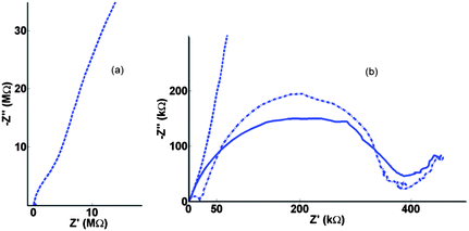 | ||
| Fig. 6 (a) Nyquist Electrochemical Impedance Spectroscopy (EIS) data for oxidation of FCA in FCA(I) solution at the 10μ3D50n electrode at Edc = +0.275 V, frequencies logarithmically spaced between 100 kHz and 0.01 Hz and an ac perturbation of 10 mV. (b) Same data on an expanded scale for background electrolyte (dashed line), redox solution (solid line) and the subtracted impedance (dash dotted line). | ||
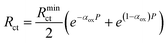
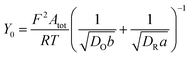
Considering Z (Fig. 7a), two zones are apparent as shown; in the higher frequency zone the diffusion layer is thin compared to the microsquare spacing and each microsquare responds independently. In the lower frequency zone, the 45° Warburg line is diagnostic of complete overlap of neighbouring diffusion layers and linear diffusion to the entire electrode array. Previous work for a single microsquare electrode53 has shown that, through the use of transmission line theory, the fundamental redox response reduces with a reasonable level of accuracy to the modified Randles circuit (Fig. 4c). The circuit elements then represent physical parameters: the electrolyte resistance (Rel), non-Faradaic microelectrode double-layer capacitance (Cdl), charge transfer resistance (Rct) determined by the electron transfer rate of the redox reaction, the Warburg (W) element (whose parameter Y0 is determined by the redox concentration and diffusion coefficient) and the non-linear resistance (Rnl) corresponding to the steady-state hemispherical diffusion limited current. It might be expected that in the higher frequency (single electrode) zone, when the electrodes behave independently (Zsingle = NZ), the impedance data, Z, for the redox response of the N MNEE apertures could be modelled using this circuit. However, the data fit better to a variant of this circuit (Fig. 4d), where the Warburg element is replaced by a redox capacitance (CN). The physical origins of this difference are interesting. We postulate this to be the enhanced non-linear diffusional transport to the nanoband edges, which gives rise to the rapid redox conversion of the volume of solution above each microsquare,9–12,68 and which is best modelled in a single parameter by the capacitance, CN. Steady-state hemispherical diffusional transport (determined by Rnl) then occurs into this volume as for the microsquare. Fig. 7b–d show the close fit of the impedance data to this relatively simple circuit, and to the predicted variation of the extracted parameters (see EIS theory section below) with the applied dc potential, Edc. The main fit variance is in the CN, Rnl near-semicircular region and can be attributed to the small deviation seen due to enhanced corner diffusion in microsquares53 and the neglect of any diffusional contribution to CN; these are approximations that have been made to restrict the number of fit parameters.
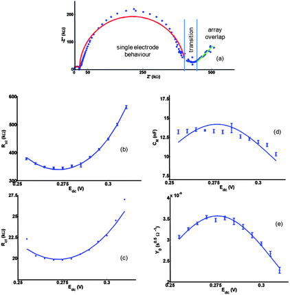 | ||
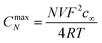
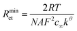
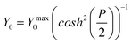
| Fig. 7 (a) Typical subtracted Nyquist Electrochemical Impedance Spectroscopy (EIS) data at the 10μ3D50n electrode for oxidation of FCA(I) solution at Edc = +0.290 V. Also shown are theoretical fits to the circuit in Fig. 4c and to the circuit (resistance in series with Warburg element) appropriate at low frequency when there is complete diffusional array overlap. Fits (solid lines) to the (b) Rnl (c) Rct (d) CN (e) Y0 data extracted from iterative fitting to the EIS measurements at each Edc performed using either Matlab (The Mathworks, Natick, Massachusetts, USA) or Nova (Version 1.9, Metrohm Autolab B.V., Utrecht, The Netherlands). The fits of these data to eqn (3), (8), (10) and (13), (lines shown in (b), (c), (d) and (e)) gave the following global values: E′ = 0.273 ± 0.002 V; Rctmin = 19.87 ± 0.06 kΩ; Rnlmin = 339 ±1 kΩ; CNmax = 14.3 ± 0.3 nF, Y0max = 35.7 ± 0.2 μs0.5 Ω−1. | ||
When considering fit parameter values, the insensitivity of Cdl to Edc is expected, but it is interesting that Cdl, per unit geometric area, at 0.94 μF cm−2 is an order of magnitude smaller than that expected for a platinum macroelectrode double layer capacitance, which suggests a thicker nanoelectrode double layer. This could be a nano effect, as electrodes of smaller than 100 nm are thought to show screening over greater distances than larger electrodes, due to enhanced ion transport in the double layer; the change from planar to hemispherical geometry fields,69 and/or the suggestion that ion size is no longer negligible.70 The value of E′ = 273 mV is also consistent with measured half-wave potential values at a rotating disc macroelectrode and previously reported measurements at similar pH.66 Similarly, the value of D obtained from eqn (14) and EIS studies (D = (2.13 ± 0.02) × 10−6 cm2 s−1) agrees well with that obtained from voltammetry. The CNmax value is calculated to correspond to complete redox conversion of a hemispherical volume of solution of radius 13.5 μm centred on each microsquare, which is consistent with the diffusion layer thickness produced by simulation (Fig. 2c).
Previously, widely varying values for kθ of FCA have been reported, ranging from 2.48 × 10⁻³ cm s−1 in 0.1 M potassium chloride and 0.2 M phosphate buffer (pH 7.4) on glassy carbon71 to 1.4–3.6 cm s−1 in acetonitrile electrolyte on Pt microdisks.72 A value of 0.850 ± 0.003 cm s−1 was extracted from the impedance data and eqn (9), which confirms that the enhanced MNEE diffusion, like other nanoelectrode systems, makes this system capable of the precise and quantitative measurement of rapid electrochemical kinetics. The enhanced diffusional transport to the MNEE system also makes it relatively insensitive to the effects of chaotic convection (Fig. 8), opening up the prospect of quantitative analytical measurement in such systems.
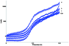 | ||
| Fig. 8 Cyclic voltammograms recorded in highly stirred solution on 10μ3D50n for 0.1 mM FCA in FCA(I) without background subtraction. The solution was stirred chaotically by using a small electric whisk at high rotation speed. The scan rates were v = (a) 200 mV s−1, (b) 100 mV s−1, (c) 20 mV s−1, (d) 10 mV s−1 and (e) 2 mV s−1. | ||
5. Nanoelectrode effects
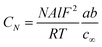
Having established the fundamental response of the MNEE system, the production and characterisation of systems with systematic control of dimensional parameters has been employed to further probe their electroanalytical response, in particular determining whether and under what conditions nanoscale electrode effects are significant. Fig. 9 shows the typical response of a 20μ3D50n device when oxidizing FCA in FCA solution and in FCA(I/10) solution.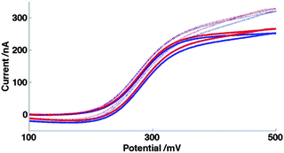 | ||
| Fig. 9 CVs for oxidation on 20μ3D50n of 0.10 mM FCA in FCA(I) (solid) and FCA(I/10) solution (dashed). These voltammograms are shown at sweep rates of 50 mV s−1 (blue) and 100 mV s−1 (red). | ||
It is clear from these voltammograms that there is a small but significant difference, with an increased current seen in both voltammograms at lower ionic strength. All voltammograms also show a linear increase with potential in the region of mass transfer limited current at both low and high ionic strength. Equivalent voltammograms are also shown for this device for HAR reduction (Fig. 10); the effect is even more marked for this system, with the increase in current on reducing ionic strength and decreasing potential for this reduction being proportionally greater than seen for FCA oxidation.
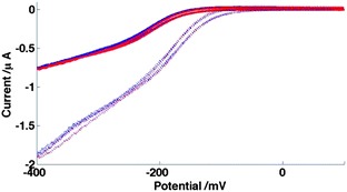 | ||
| Fig. 10 CVs for reduction on 20μ3D50n of 0.10 mM HAR in HAR(I) (solid) and HAR(I/50) solution (dashed). These voltammograms are again shown at sweep rates of 50 mV s−1 (blue) and 100 mV s−1 (red). | ||
This is consistent with potential dependent enhancement of FCA/HAR ion reagent transport to the electrode through migration (as a combination of the larger change in ionic strength and larger charge on the redox agent, 3+ for HAR reduction and 1− for FCA oxidation, for HAR than FCA, would explain the enhanced response). Migration effects have been considered previously73 for nanoscale hemispherical electrodes. In the case when the Debye length, κ−1, of the electrolyte approaches the size of the electrode, there is significant field in the diffusion layer, and migration enhances mass transfer, leading to a potential dependent increase in the current. This previous work considered such effects to be significant for 5 nm radius hemispherical nanoelectrodes when I was of the order of 200 μM and below, for which κ−1 ∼ 20 nm. Krapf et al. suggested such effects occur at a higher value of I = 0.5 M.74 In this work, for FCA(I) and FCA(I/10), I = 0.70 mol dm−3 and 0.070 mol dm−3 respectively, whilst for HAR(I) and HAR(I/50) solutions, I = 0.50 mol dm−3 and 0.01 mol dm−3 respectively, which result in values of κ−1 ranging between ∼0.3 and 2.4 nm respectively, compared to the much greater nanoelectrode width of 50 nm. At first sight it seems puzzling that such relatively small values of Debye length compared to electrode dimension can give rise to the significant migrational contribution observed, but it should be remembered that unlike hemispherical electrodes, for which the current density is constant across the electrode surface, these nanoband electrode systems display markedly asymmetric current distribution, with the very highest current densities at the band edges. It is here that the depletion layer is at its thinnest, the field lines will be most crowded and the effects of migration will be most keenly felt. This work indicates that this results in significant migrational contribution to the transport and hence the observed current at these edges even for a 50 nm nanoband, and even at these relatively large values of I.
In order to confirm that the effect is predominantly an additional migrational contribution to the mass transfer and not a field effect on the charge transfer rate constant, Fig. 11 and 12 show the corresponding EIS spectra for FCA and HAR at Edc = E′, along with their fits to the equivalent circuit, Fig. 4(d). It is clear for FCA these data at the two different values of I produce essentially the same fit parameters for all except Rnlmin, whose value has decreased by around 10% when changing from higher to lower I. For HAR, which has similarly rapid charge transfer kinetics, the difference in Rnlmin is greater, with a decrease of around 50% when changing from higher to lower I. It is reassuring that these values, when substituted into eqn (22) predict currents which correspond well to the currents observed in Fig. 9 and 10.
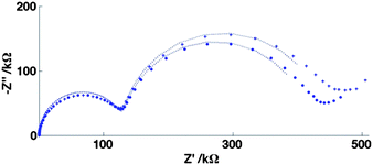 | ||
| Fig. 11 EIS data for the 20μ3D50n electrode showing the oxidation of 0.1 mM FCA in FCA(I) solution (+) and FCA(I/10) solution (•) and the corresponding fits for Edc = E′, Vac = 10 mV, for the frequency range 100 kHz to 10 mHz (logarithmic distribution). Fits: FCA(I) solution: Rct = 135 ± 1 kΩ, Cdl = 31.1 ± 0.7 nF, Rnlmin = 309 ± 3 kΩ, CN = 1.34 ± 0.02 μF, FCA(I/10) solution: Rct = 135 ± 1 kΩ, Cdl = 27.7 ± 0.6 nF, Rnlmin = 283 ± 2 kΩ, CN = 1.33 ± 0.02 μF. | ||
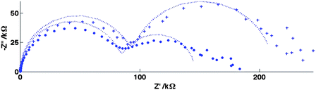 | ||
| Fig. 12 Equivalent EIS data to Fig. 11 for the 20μ3D50n electrode for the reduction of 0.10 mM HAR in HAR(I) solution (+) and HAR(I/50) solution (•) and the corresponding fits for Edc = E′. Fit values: HAR(I) solution: Rct = 96 ± 1 kΩ, Cdl = 31 ± 1 nF, Rnlmin = 116 ± 2 kΩ, CN = 2.35 ± 0.08 μF, HAR(I/50) solution: Rct = 86 ± 1 kΩ, Cdl = 27 ± 1 nF, Rnlmin = 60 ± 2 kΩ, CN = 3.0 ± 0.2 μF. | ||
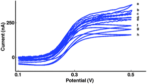
By contrast, Fig. 13a shows equivalent voltammetric data for oxidation of FCA at a 5 nm thickness nanoband, 10μ4D5n. By comparison with Fig. 13b, the equivalent 50 nm nanoband system, the currents observed at high ionic strength are ∼98% lower. Similar dramatic differences have been observed previously75,76 for linear nanoband electrodes of similar width. This has been explained by the fact that the dimension of the redox species is now comparable to the thickness of the nanoband, which results in a breakdown of applicability of the analytical equations which describe mass transport of redox species to the electrode. In this work, a model was proposed which accounted for this behaviour in terms of two effects; the first is a marked decrease in the diffusion coefficient near the electrode due to changes in the ion–solvent interaction, the solvent composition and solvent viscosity due to the fact that the electrode dimension, the depletion zone thickness and κ−1 are all comparable. The second is the fact that as the electrode dimension approaches the molecular dimension, the concentration gradient at and across the electrode surface can no longer be represented by a smooth analytical function, which has the practical effect of reducing this gradient and the resulting diffusive flux still further from that predicted analytically. In addition, however, the lower ionic strength data in Fig. 13a demonstrate a dramatic increase in the current for 10μ4D5n by a factor of around 5. It is interesting that this additional current is comparable in magnitude to that observed on decreasing I for 10μ4D50n (Fig. 13b), which is consistent with this enhanced migrational contribution being again due to migration at the band edges. The decrease in band width therefore appears to result in promotion of the importance of the band edges compared to diffusion to and reaction across the band centre (which has become a vanishingly small contribution to the current). It is also possible that there is at least some contribution to this increase in current with decreasing I which is due to the enhancement of the local electric field at the electrode with increasing potential. This could result in direct electron transfer between redox species and electrode becoming possible at greater distances from the electrode through an increase in the electron tunnelling rate,77 which could relax the requirement for short range electron transfer at the electrode surface.
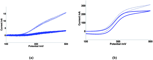 | ||
| Fig. 13 Cyclic voltammetry in FCA(I) solution (solid line) and FCA(I/10) solution (dashed line) at 20 mV s−1 of (a) 10μ4D5n (b) 10μ4D50n. | ||
6. Conclusions
This work demonstrates the MNEE array to be a sensitive electroanalytical device with enhanced characteristics. The design enables the high diffusional rate and high signal-to-noise ratio available with nanoelectrode measurements (facilitating the measurement of fast electrode kinetics) to be combined with both the steady-state response found with microelectrodes and the high total current available with arrays. Another attraction is that the sensitive quantitative response coupled with the relative insensitivity to environmental convection makes these electrodes highly suitable for quantitative electroanalysis and monitoring in systems for which well-defined stirring is either undesirable or impractical. The use of CMOS compatible microfabrication techniques provides the possibility of integrating these devices with control and measurement circuitry, in the so-called “More than Moore” approach.78,79 The photolithographic method of their fabrication also enables reproducible production and systematic variation of such factors such as band thickness (width) and placement, hole dimension and separation. This work also indicates that they provide a suitable platform for measuring and understanding nanoelectrode effects. Nanoband systems of 50 nm thickness are demonstrated to be sufficiently thin to provide enhanced nanoelectrode characteristics, albeit that their response shows some migrational transport contribution at all but the highest ionic strengths. Nanoband systems of 5 nm thickness show lower currents and increased relative migrational effects, consistent with previously postulated effects of finite redox ion size on the nanoband dimension.7. EIS theory
Previous work has modelled the EIS behaviour of microelectrodes of varying sizes and geometries. A method to extract the diffusional impedance of a microdisc from the chronoamperometric current80 was extended to microbands of various ideal and non-ideal geometries.81,82 Gabrielli et al. used FEMLAB (a predecessor of COMSOL) to simulate the EIS response of a microdisc.83This work develops an analytical description for the MNEE. Previous work9–12,68 has shown the variation of CN with the concentrations of the two forms of a one electron redox couple (e.g. reduced and oxidised FCA), a and b in the volume of solution above the microsquares should be given by
 | (3) |
 | (4) |
 | (5) |
 | (6) |
 | (7) |
The equations for the potential dependence of Rnl, and Rct for single microsquares have been derived previously;53 when combined with the fact that for an array of N parallel independent circuit elements, Rarray = Rsingle/N; Carray = NCsingle, this gives
 | (8) |
 | (9) |
As shown previously53
 | (10) |
 | (11) |
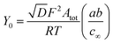
Assuming that the diffusion coefficients of the oxidized, DO, and reduced, DR, redox species are equal and given by D
 | (12) |
 | (13) |
 | (14) |
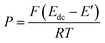
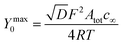
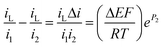
In order to relate the mass transfer limited current, iL, to Rnl, the modified Tafel equation, shown to be applicable to a reversible one electron transfer at these electrodes (Fig. 14)
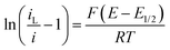 | (15) |
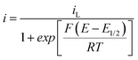 | (16) |
 | (17) |
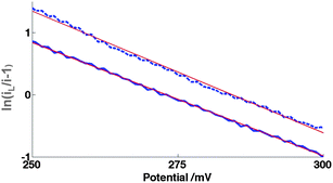 | ||
| Fig. 14 Modified Tafel plot (eqn (15)) from CV, Fig. 4, for 10μ3D50n for 0.10 mM FCA oxidation in FCA(I) for oxidative (solid) and reductive (dashed) sweeps at v = 100 mV s−1. The Tafel slopes are 37 and 39 V−1 respectively by linear regression; the theoretical value is 39 V−1 from eqn (15) at T = 298 K. | ||
For this small potential change, eqn (17) becomes
 | (18) |
The resulting impedance is then the non-linear resistance under these conditions
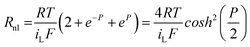
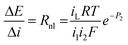 | (19) |
When ΔE is small
 | (20) |
Combining eqn (19) and (20) then gives
 | (21) |
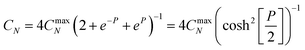
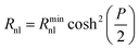
Thus when cosh2(P/2) = 1 (P = 0, or Edc = E1/2 = E′), the value of Rnl is equal to Rnlmin, the minimum non-linear resistance, which is related to iL through
 | (22) |
Acknowledgements
The School of Chemistry at Edinburgh is celebrating 300 years of Chemistry at Edinburgh and is part of the EaStCHEM joint chemistry research school with St Andrews. The Institute for Integrated Micro and Nano Systems is part of the Institute for Integrated Systems (a Joint Research Institute with Heriot-Watt University as part of the Edinburgh Research Partnership in Engineering and Mathematics (ERPem)). Support from the Scottish Funding Council is acknowledged for the ERPem and EaStCHEM initiatives, along with knowledge transfer funding. Support from EPSRC/IeMRC is also acknowledged and IS and HLW thank EPSRC and the University of Edinburgh for financial support.References
- J. Heinze, Angew. Chem., Int. Ed. Engl., 1993, 32, 1268–1288 CrossRef
.
- R. J. Forster, Chem. Soc. Rev., 1994, 23, 289–297 RSC
- K. Stulik, C. Amatore, K. Holub, V. Marecek and W. Kutner, Pure Appl. Chem., 2000, 72, 1483–1492 CrossRef CAS
- A. J. Bard and L. R. Faulkner, Electrochemical methods, 2nd ed., Wiley, New York, 2001, pp. 168–176 Search PubMed
- C. Batchelor-McAuley, E. J. F. Dickinson, N. V. Rees, K. E. Toghill and R. G. Compton, Anal. Chem., 2012, 84, 669–684 CrossRef CAS
- C. Amatore, C. Pebay, L. Thouin, A. Wang and J.-S. Warkocz, Anal. Chem., 2010, 82, 6933–6939 CrossRef CAS
- J. T. Cox and B. Zhang, Annu. Rev. Anal. Chem., 2012, 5, 253–272 CrossRef CAS
- A. M. Bond, Analyst, 1994, 119, 1R–21R RSC
- Y. Tu, Y. Lin and Z. F. Ren, Nano Lett., 2003, 3, 107–109 CrossRef CAS
- I. Heller, J. Kong, H. A. Heering, K. A. Williams, S. G. Lemay and C. Dekker, Nano Lett., 2005, 5, 137–142 CrossRef CAS
- D. Wei, Y. Liu, L. Cao, Y. Wang, H. Zhang and G. Yu, Nano Lett., 2008, 8, 1625–1630 CrossRef CAS
- D. W. M. Arrigan, Analyst, 2004, 129, 1157–1165 RSC
- R. G. Compton, G. G. Wildgoose, N. V. Rees, I. Streeter and R. Baron, Chem. Phys. Lett., 2008, 459, 1–17 CrossRef CAS
- R. W. Murray, Chem. Rev., 2008, 108, 2688–2720 CrossRef CAS
- J. M. Pingarron and P. Yanez-Sedeno, Curr. Top. Electrochem., 2003, 9, 165–176 Search PubMed
- R. Feeney and S. P. Kounaves, Electroanalysis, 2000, 12, 677–684 CrossRef CAS
- C. A. Amatore, Spectra 2000, 1990, 151, 43–46 CAS
- M. Fleischmann and S. Pons, Anal. Chem., 1987, 59, 1391A–1399A CrossRef CAS
- J. O. Howell, Curr. Sep., 1987, 8, 2–16 CAS
- K. Gerasopoulos, X. Chen, J. Culver, C. Wang and R. Ghodssi, Chem. Commun., 2010, 46, 7349–7351 RSC
- M. A. Alonso-Lomillo, O. Rüdiger, A. Maroto-Valiente, M. Velez, I. Rodríguez-Ramos, F. J. Muñoz, V. M. Fernández and A. L. De Lacey, Nano Lett., 2007, 7, 1603–1608 CrossRef CAS
- C. Koenigsmann, W.-P. Zhou, R. R. Adzic, E. Sutter and S. S. Wong, Nano Lett., 2010, 10, 2806–2811 CrossRef CAS
- D. Zhan, J. Velmurugan and M. V. Mirkin, J. Am. Chem. Soc., 2009, 131, 14756–14760 CrossRef CAS
- R. Hu, B. A. Cola, N. Haram, J. N. Barisci, S. Lee, S. Stoughton, G. Wallace, C. Too, M. Thomas and A. Gestos, et al., Nano Lett., 2010, 10, 838–846 CrossRef CAS
- Q. Li and R. M. Penner, Nano Lett., 2005, 5, 1720–1725 CrossRef CAS
- D. Gu, H. Baumgart and G. Namkoong, Phys. Status Solidi RRL, 2011, 5, 104–106 CrossRef CAS
- I. Heller, J. Kong, H. A. Heering, K. A. Williams, S. G. Lemay and C. Decker, Nano Lett., 2005, 5, 137–142 CrossRef CAS
- A. C. Barton, S. D. Collyer, F. Davis, D. D. Gornall, K. A. Lawa, E. C. D. Lawrence, D. W. Mills, S. Myler, J. A. Pritchard, M. Thompson and S. P. J. Higson, Biosens. Bioelectron., 2004, 20, 328–337 CrossRef CAS
- M. S. Doescher, U. Evans, P. E. Colavita, P. G. Miney and M. L. Myricks, Electrochem. Solid-State Lett., 2003, 6, C112–C115 CrossRef CAS
- R. M. Penner and C. R. Martin, Anal. Chem., 1987, 59, 2625–2630 CrossRef CAS
- U. Evans, P. E. Colavita, M. S. Doescher, M. Schiza and M. L. Myricks, Nano Lett., 2002, 2, 641–645 CrossRef CAS
- S. Viswanathan, C. Rani, S. Ribeiro and C. Delerue-Matos, Biosens. Bioelectron., 2012, 33, 179–183 CrossRef CAS
- P. Ugo, L. M. Moretto, M. De Leo, A. P. Doherty, C. Vallese and S. Pentlavalli, Electrochim. Acta, 2010, 55, 2865–2872 CrossRef CAS
- M. Faustini, B. Marmiroli, L. Malfatti, B. Louis, N. Krins, P. Falcaro, G. Grenci, C. Laberty-Robert, H. Amenitsch, P. Innocenzic and D. Grosso, J. Mater. Chem., 2011, 21, 3597–3603 RSC
- S. P. Branangan, N. M. Contento and P. W. Bohn, J. Am. Chem. Soc., 2012, 134, 8617–8624 CrossRef
- M. Manheller, S. Trellenkamp, R. Waser and S. Karthäuser, Nanotechnology, 2012, 23, 125302–125305 CrossRef
- M. E. Sandison and J. M. Cooper, Lab Chip, 2006, 6, 1020–1025 RSC
- M. P. Nagale and I. Fritsch, Anal. Chem., 1998, 70, 2902–2907 CrossRef CAS
- M. P. Nagale and I. Fritsch, Anal. Chem., 1998, 70, 2908–2913 CrossRef CAS
- E. J. Menke, M. A. Thompson, C. Xiang, C. Yang and R. M. Penner, Nat. Mater., 2006, 5, 914–919 CrossRef CAS
- C. Xiang, S.-C. Kung, D. K. Taggart, F. Yang, M. A. Thompson, A. G. Guell, Y. Yang and R. M. Penner, ACS Nano, 2008, 2, 1939–1949 CrossRef CAS
- F. Yang, D. Jung and R. M. Penner, Anal. Chem., 2011, 83, 9472–9477 CrossRef CAS
- N. A. M. Said, K. Twomey, V. I. Ogurtsov, D. W. M. Arrigan and G. Herzog, J. Phys.: Conf. Ser., 2011, 307, 012052 CrossRef
- E. Jeoung, T. H. Galow, J. Schotter, M. Bal, A. Ursache, M. T. Tuominen, C. M. Stafford, T. P. Russell and V. M. Rotello, Langmuir, 2001, 17, 6396–6398 CrossRef CAS
- J. Koehne, J. Li, A. M. Cassell, H. Chen, Q. Ye, H. T. Ng, J. Han and M. Meyyappan, J. Mater. Chem., 2004, 14, 676–684 RSC
- K. Wang, H. A. Fishman, H. Dai and J. S. Harris, Nano Lett., 2006, 6, 2043–2048 CrossRef CAS
- N. Yang, H. Uetsuka, E. Osawa and C. E. Nebel, Nano Lett., 2008, 8, 3572–3576 CrossRef CAS
- M. D. Dickey, D. J. Lipomi, P. J. Bracher and G. M. Whitesides, Nano Lett., 2008, 8, 4568–4573 CrossRef CAS
- Q. Xu, R. M. Rioux, M. D. Dickey and G. M. Whitesides, Acc. Chem. Res., 2008, 41, 1566–1577 CrossRef CAS
- N. J. Freeman and A. R. Mount, Microelectrode System, PCT WO99/60392A1 Search PubMed.
- J. G. Terry, I. Underwood, I. Schmueser, A. S. Bunting, A. R. Mount, N. J. Freeman and A. J. Walton, IET Nanobiotechnology, to be submitted, 2013 Search PubMed
- N. J. Freeman, R. Sultana, N. Reza, H. Woodvine, J. G. Terry, A. J. Walton, C. L. Brady, I. Schmueser and A. R. Mount, Phys. Chem. Chem. Phys., 2013, 15, 8112–8118 RSC
- H. L. Woodvine, J. G. Terry, A. J. Walton and A. R. Mount, Analyst, 2010, 135, 1058–1065 RSC
- J. A. Alden and R. G. Compton, J. Phys. Chem. B, 1997, 101, 8941–8954 CrossRef CAS
- J. B. Flanagan and L. Marcoux, J. Phys. Chem., 1973, 77, 1051–105 CrossRef CAS
- J. A. Alden, J. Booth, R. G. Compton, R. A. W. Dryfe and G. H. W. Sanders, J. Electroanal. Chem., 1995, 389, 45–54 CrossRef
- I. J. Cutress, E. J. F. Dickinson and R. G. Compton, J. Electroanal. Chem., 2010, 638, 76–83 CrossRef CAS
- J. A. Alden and R. G. Compton, J. Electroanal. Chem., 1996, 402, 1–10 CrossRef
- C. A. Basha and L. Rajendran, Int. J. Electrochem. Sci., 2006, 1, 268–282 CAS
- J. Guo and E. Lindner, Anal. Chem., 2009, 81, 130–138 CrossRef CAS
- T. J. Davies and R. G. Compton, J. Electroanal. Chem., 2005, 502, 177–187 Search PubMed
- D. Britz, K. Poulsen and J. Strutwolf, Electrochim. Acta, 2004, 50, 107–113 CrossRef CAS
- K. B. Oldham, Electrochem. Commun., 2004, 6, 210–214 CrossRef CAS
- C. Amatore, Physical Electrochemistry: Principles, Methods and Applications, I. Rubinstein, Ed., Marcel Dekker, New York, 1995, pp. 131–208 Search PubMed
- K. Aoki, Electroanalysis, 1993, 5, 627–639 CrossRef CAS
- A. Berduque, Y. H. Lanyon, V. Beni, G. Herzog, Y. E. Watson, K. Rodgers, F. Stam, J. Alderman and D. W. M. Arrigan, Talanta, 2007, 71, 1022–1030 CrossRef CAS
- M. Fleishmann and S. Bandyopadhyay, J. Phys. Chem., 1985, 89, 5537–5541 CrossRef
- A. R. Mount and M. T. Robertson, Phys. Chem. Chem. Phys., 1999, 1, 5169–5177 RSC
- R. He, S. Chen, F. Yang and B. Wu, J. Phys. Chem. B, 2006, 110, 3262–3270 CrossRef CAS
- C. P. Smith and H. S. White, Anal. Chem., 1993, 65, 3343–3353 CrossRef CAS
- M. D. Osborne, B. J. Seddon, R. A. W. Dryfe, G. Lagger, U. Loyall, H. Schäfer and H. H. Girault, J. Electroanal. Chem., 1996, 417, 5–15 CrossRef CAS
- A. M. Bond, T. L. E. Henderson, D. R. Mann, T. F. Mann, W. Thormann and C. G. Zoski, Anal. Chem., 1988, 60, 1878–1882 CrossRef CAS
- J. J. Watkins, B. Zhang and H. S. White, J. Chem. Educ., 2005, 82, 712–719 CrossRef CAS
- D. Krapf, B. M. Quinn, M.-Y. Wu, H. W. Zandbergen, C. Dekker and S. G. Lemay, Nano Lett., 2006, 6, 2531–2535 CrossRef CAS
- R. B. Morris, D. J. Franta and H. S. White, J. Phys. Chem., 1987, 91, 3559–3564 CrossRef CAS
- J. D. Seibold, E. R. Scott and H. S. White, J. Electroanal. Chem., 1989, 264, 281–289 CrossRef CAS
- R. J. White and H. S. White, Langmuir, 2008, 24, 2850–2855 CrossRef CAS
- M. Lapisa, G. Stemme and F. Niklaus, IEEE J. Sel. Top. Quantum Electron., 2011, 17, 629–644 CrossRef CAS
- A. J. Walton, J. T. M. Stevenson, I. Underwood, J. G. Terry, S. Smith, W. Parkes, C. Dunare, H. Lin, Y. Li, R. Henderson, D. Renshaw, B. Rae, K. Muir, M. Desmulliez, D. Flynn, M. J. MacIntosh, W. S. Holland, A. F. Murray, T. B. Tang and A. S. Bunting, SAIEE Res. J., 2010, 10, 3–10 Search PubMed
- A. Bezegh and J. Janata, J. Electroanal. Chem., 1986, 215, 139 CrossRef CAS
- R. G. Compton and J. Winkler, J. Phys. Chem., 1995, 99, 5029 CrossRef CAS
- J. A. Alden and R. G. Compton, Electroanalysis, 1996, 8, 30–33 CrossRef CAS
- C. Gabrielli, M. Keddam, P. Rousseau and V. Vivier, Numerical Simulation of the Electrochemical Impedance of a Microelectrode using FEMLAB, Excerpt from the Proceedings of the COMSOL Multiphysics User's Conference, 2005, Paris Search PubMed
| This journal is © The Royal Society of Chemistry 2013 |