 Open Access Article
 This Open Access Article is licensed under a
 Creative Commons Attribution 3.0 Unported Licence
Networks of DNA-templated palladium nanowires: structural and electrical characterisation and their use as hydrogen gas sensors
Mariam N. Al-Hinai†
ac,
Reda Hassanienb,
Nicholas G. Wrightc,
Alton B. Horsfallc,
Andrew Houltona and
Benjamin R. Horrocks*a
aChemical Nanoscience Laboratory, School of Chemistry, Newcastle University, Bedson Building, NE1 7RU, UK. E-mail: b.r.horrocks@ncl.ac.uk; Tel: +44(0)191 2225619
bDepartment of Science and Mathematics, Faculty of Education, Assiut University, New Valley Branch, El-Kharja 72511, Egypt
cSchool of Electrical and Electronic Engineering, Newcastle University, Merz Court, NE1 7RU, UK
First published on 4th March 2013
Abstract
Electroless templating on DNA is established as a means to prepare high aspect ratio nanowires via aqueous reactions at room temperature. In this report we show how Pd nanowires with extremely small grain sizes (<2 nm) can be prepared by reduction of PdCl42− in the presence of λ-DNA. In AFM images the wires are smooth and uniform in appearance, but the grain size estimated by the Scherrer treatment of line broadening in X-ray diffraction is less than the diameter of the wires from AFM (of order 10 nm). Electrical characterisation of single nanowires by conductive AFM shows ohmic behaviour, but with high contact resistances and a resistivity (∼10−2 Ω cm) much higher than the bulk value for Pd metal (∼10−5 Ω cm @20 °C). These observations can be accounted for by a model of the nanowire growth mechanism which naturally leads to the formation of a granular metal. Using a simple combing technique with control of the surface hydrophilicity, DNA-templated Pd nanowires have also been prepared as networks on an Si/SiO2 substrate. These networks are highly convenient for the preparation of two-terminal electronic sensors for the detection of hydrogen gas. The response of these hydrogen sensors is presented and a model of the sensor response in terms of the diffusion of hydrogen into the nanowires is described. The granular structure of the nanowires makes them relatively poor conductors, but they retain a useful sensitivity to hydrogen gas.
1 Introduction
Controlled fabrication of materials with a specific shape or size remains an important topic in nanotechnology. Nanowires are of particular interest for the fabrication of functional electronic devices and duplex DNA has been shown to be highly effective for promoting the anisotropic growth of a variety of materials such as organic conducting polymers,1–8 metals,9–23 metal oxides,24–26 semiconducting chalcogenides,27–30 and superconducting alloys.31 The self-assembly and molecular recognition abilities of DNA may also alleviate the problems of inter-element wiring and positioning at the nanometer scale.32 The templating reaction proceeds by the formation of nuclei on the template and these nuclei grow and may eventually overlap.33 The resulting structure is typically either in the form of a smooth nanowire or a series of beads on a string. DNA-templated nanowires have several advantages: ease of fabrication, deposition and controlled alignment on a substrate by molecular combing.4,27 They are therefore of particular interest in sensing technology.It is now widely recognised that hydrogen gas sensors are essential for safety reasons in any widespread use of hydrogen as a low-carbon energy source.34,35 Hydrogen is highly flammable and becomes explosive when its concentration exceeds 4% in air.36 The sensors are required to be rapid, sensitive, reliable, cheap, simple to operate and to have high selectivity. The required selectivity can be obtained by using the ability of palladium to sorb hydrogen gas.37 Electronic sensors have advantages over optical and other devices with respect to the simplicity of the sensor structures and compatibility of the sensor fabrication process with miniaturization and the current IC process.38 However, bulk Pd-based hydrogen sensors suffer from fundamental problems including long diffusion-limited response times and irreversible resistance changes resulting from the large internal stress caused by the expansion that occurs upon excess hydrogen absorption.39 Sensors have therefore been designed using various Pd-based nanomaterials, including nanowires, as transducers.40–54 Interest in nanowires for use in sensor technology has grown and therefore Pd/DNA nanowires may be attractive for hydrogen sensing. In particular, DNA-templated nanowires offer a simple and cost effective sensor fabrication process. In this report we describe the chemical and structural characterisation of Pd/DNA nanowires, their electrical behaviour and discuss the response of a Pd/DNA nanowire network as a hydrogen sensor.
2 Experimental
2.1 Preparation of Pd/DNA nanowires
Palladium nanowires (Pd/DNA) were prepared by templating the electroless reduction of Pd(II) on lambda DNA (λ-DNA) or calf thymus DNA (CT-DNA). λ-DNA was purchased from New England Biolabs (cat. no. N30011S Hitch, Herts, UK) at a concentration of 500 ng μL−1 in pH 8 buffer; it was used as supplied. CT-DNA was obtained from Sigma-Aldrich (highly polymerised, 6% sodium). All other reagents were obtained from Sigma-Aldrich and were of AnalaR grade or equivalent. Deionized water was obtained from a Barnstead nanopure™ purification train with nominal resistivity of 18.2 MΩ cm.Our standard preparation of Pd/DNA nanowires:
10 μL of freshly-prepared K2PdCl4(aq) (3 mM) was added to 20 μL of λ-DNA (500 ng μL−1) in the presence of 5 μL sodium citrate (aq) (0.5 mM). The Pd(II) ions were reduced to Pd(0) metal by addition of 5 μL aqueous dimethylaminoborane (DMAB, 10 mM) or NaBH4 (10 mM). The solution was thoroughly mixed and allowed to react at room temperature for 2–24 h as indicated in the results section. 24 h reaction times were required to form smooth continuous nanowires. Use of NaBH4 or DMAB as reducing agent produced similar nanowires; some differences between the two are noted in the electrical characterisation below.
Slightly different preparation methods were used for UV-Vis spectroscopy and XRD analysis because these techniques require larger samples. CT-DNA was employed for reasons of cost.
For UV-Vis experiments:
2 mL aqueous CT-DNA (162.5 ng μL−1) was mixed with 1 mL freshly-prepared K2PdCl4 (aq) (3 mM) in the presence of 0.5 mL sodium citrate (aq) (0.5 mM). 0.5 mL of aqueous dimethylaminoborane (DMAB, 10 mM) was added dropwise to the pale yellow solution.
For XRD experiments:
Half the quantities employed in the UV-Vis experiment were used. A black precipitate of Pd/DNA was formed and was collected by filtration and washed thoroughly with hot ethanol.
2.2 FTIR spectroscopy
FTIR spectra (in the range 800–1800 cm−1) were recorded in transmission mode with a Bio-Rad Excalibur FTS-40 spectrometer (Varian Inc., Palo Alto, CA, USA) equipped with a liquid nitrogen cooled deuterated triglycine sulphate (DTGS) detector. 128 scans were co-added and averaged and the resolution was 4 cm−1. Pd/DNA solution (8 μL) was deposited on a clean p-Si(100) chip (1 cm × 1 cm) and dried in air for 1 h prior to analysis. A clean p-Si(100) chip served as the background.2.3 UV-Vis spectroscopy
Ultraviolet-visible (UV-Vis) absorption spectroscopy was employed to monitor the reaction progress. UV-Vis absorbance spectra of Pd nanowires before and after DMAB reduction were recorded in situ on a Thermo Spectronic GENESYS 6 spectrophotometer at room temperature (wavelength range: 250 to 600 nm).2.4 X-ray photoelectron spectroscopy
An Axis-Ultra photoelectron spectrometer equipped with a monochromatic Al-Kα X-ray as the excitation source (1486.7 eV) with an operating power of 150 W (15 kV, 10 mA) was used to collect photoemission spectra of Pd–DNA samples. The photoelectrons were filtered by the hemispherical analyzer and recorded by multi-channel detectors. The chamber pressure was 3.2 × 10⁻⁹ Torr. For the survey scan, the pass energy was 20 eV and the step size was 0.3 eV. The binding energies obtained in the XPS analysis were calibrated using C1s (284.6 eV) as a reference. Spectral peaks were fitted with mixed singlet functions or a Doniach–Sunjic doublet function after subtraction of a Shirley-type background using the WinSpec program developed by LISE laboratory, Belgium. The Pd/DNA samples were prepared by depositing 8 μL of solution on a clean Si(100) substrate and drying in air at room temperature in a laminar flow hood to minimize contamination (Model VLF 4B, Envair, Haslingden, Lancs, U.K.).2.5 X-ray diffraction
The XRD analysis was recorded from a powder sample using X-ray diffractometer system (XPERT-PRO) with graphite monochromatized Cu Kβ radiation (λ = 0.15418 nm). The scanning rate of 0.033° s−1 was applied to record the pattern in the 2θ range of 25° to 90°.2.6 Atomic force microscopy, conductive AFM and scanning conductance microscopy
Tapping mode imaging of surface topography was performed in air on a Multimode Dimension Nanoscope V (Veeco Instruments Inc., Metrology Group, Santa Barbara, CA, USA) using TESP7 probes (n-doped Si cantilevers, Veeco Instruments Inc., Metrology Group), with a resonant frequency of 234–287 kHz and a spring constant of 20–80 N m−1. Data acquisition was carried out using Nanoscope version 7.00b19 (Dimension Nanoscope V) software (Veeco Instruments Inc.). Vibrational noise was reduced with an isolation table/acoustic enclosure (Veeco Inc., Metrology Group). Si(100) chips (1 cm × 1 cm) cut from 100 mm diameter wafer (B-doped, p-type single-side polished; Compart Technology, Cambridge, UK) were used as substrates. The substrate was degreased by immersion in boiling organic solvents (acetone and 2-propanol) for 7 min, then rinsed with water and dried in a stream of nitrogen before silanization. Some chips were rendered hydrophobic by exposure to Me3SiCl vapour for 5–7 min. This procedure reduces the number of nanowires that adhere to the substrate when a drop of Pd/DNA solution is placed on the chip. Low nanowire densities facilitate the study of individual nanowires and also the molecular combing process by which they are aligned as the drop of solution is dragged across the surface. Omission of the silanization treatment resulted in the formation of nanowire networks, which were also investigated.Scanning conductance microscopy (SCM) measurements were carried out in air on the same Dimension Nanoscope V system using MESP probes (n-doped Si cantilevers, with a metallic Co/Cr coating, Veeco Instruments Inc., Metrology Group), with a resonant frequency of ca. 70 kHz, a quality factor of 200–260 and a spring constant of 1–5 N m−1. In SCM experiments, a bias voltage is applied between the tip and substrate. No dc current flows because the substrate is coated with a dielectric, but an electrostatic field is produced between the tip and the substrate. The phase angle between the tip motion and the driving force is related to the force gradient at the tip and is sensitive to the conductance of samples resting on the dielectric as well as their polarizability. The reported SCM phase images show the phase of the tip oscillation at a set lift height above the substrate surface (10–100 nm typ.). The substrates comprised p++Si(100) chips with a thermally grown oxide layer (240 nm) as determined by a spectrometric thin film analyzer (Filmetrics F40).
For conductive AFM (c-AFM) measurements, a constant bias was also applied between the tip and the sample (the tip was grounded). We have previously shown that DNA-templated nanowires facilitate a simple means of making contacts to individual nanowires.4 Briefly, a large amount of nanowires are deposited on the substrate by drop-casting; as the droplet dries, individual nanowires protrude from the main mass of nanowires and are aligned by the receding meniscus. Individual nanowires can be easily imaged by AFM at the edge of the dried mass. Electrical contact to the mass of nanowires was made by applying a drop of In/Ga eutectic to one corner of the chip and to the metallic chuck. c-AFM imaging was performed in contact mode, with an applied bias of 0.5 V. The imaged area was about 1 mm away from the In/Ga contact. The closed loop system of the Dimension V instrument makes it possible to reproducibly position the tip at a point of interest identified in the image of a single Pd/DNA nanowire and to record current–voltage (I–V) curves at that point. The conductance was estimated using the slope of the I–V curve at zero bias.
2.7 High-resolution transmission electron microscopy (HRTEM)
The samples for HRTEM and EDS (energy dispersive X-ray spectroscopy) were prepared by placing a drop of the Pd/DNA nanowires solution onto a carbon-coated Cu grid followed by slow evaporation of water under ambient conditions. The TEM images were acquired using a high resolution analytical field emission microscope (HR-FETEM, JEOL JEM-2100F) at Sultan Qaboos University (Oman) at an accelerating voltage of 200 kV and the EDS spectrum was recorded during the TEM experiment.2.8 Electrical characterisation
Two-terminal conductivity measurements were performed using gold microelectrodes fabricated on clean oxidised silicon using a standard reverse photolithography process. The electrode pattern consists of 8 pairs of large gold pads with 2 μm-wide fingers. The gap between each pair of fingers ranged from none to several micrometers and the two pads in each pair are separated by ≃80 μm. The two small gold fingers in each pair provide contacts to the DNA-templated Pd wires and the two large gold pads serve as electrical contacts for external measurement of the system. The Au microelectrodes were deposited in 100 nm-deep trenches produced by reactive ion etching of the SiO2. The amount of deposited Au was controlled so that the surface of the Au microelectrodes is level with the surrounding oxide surface; this enables the alignment and AFM imaging of nanowires across the fingers. In order to study single nanowires, the oxide layer was treated with Me3SiCl vapour to facilitate molecular combing. A 2 μL drop of an aqueous solution of Pd/DNA nanowires was placed on these electrodes and nanowires were aligned across the gap between the Au fingers by molecular combing. To obtain Pd/DNA nanowire networks, the Me3SiCl treatment was omitted. Electrical measurements were made using a probing station (Cascade Microtech) and a B1500A semiconductor analyser (Agilent). All of the electrical measurements were carried out under dry nitrogen without light illumination. I–V curves at various temperatures were performed on the probe station using a thermal chuck system (Model ETC-200L, ESPEC, Japan).2.9 Hydrogen sensing
To evaluate the Pd/DNA nanowire networks as hydrogen gas sensors, Pd/DNA nanowires were combed on clean Si/SiO2 substrates on which microfabricated Au electrodes had previously been fabricated. The nanowires adhere strongly to the hydrophilic SiO2 surface to form a network of interconnected nanowires. Such nanowire networks have the advantage of having multiple routes for current flow within the active sensor element, but, more importantly, between the nanowire network and the contact pads. This creates a significantly more robust and resilient device than a single nanowire sensor. The device was then connected to a sample holder by wire bonding and then placed in the chamber of the H2 gas sensing system. The system was composed of a vacuum chamber with heatable sample holder, controlled by a Lakeshore 331 temperature controller, a Keithley 6487 picoammeter for I–V measurements and cylinders of pure N2 and 2.5% H2 in N2 to modify the ambient. The chamber was initially evacuated to a base pressure of about 9 × 10⁻² Torr and then N2 was injected using a mass flow controller to create an inert ambient for control tests. Following this, the sensing gas (2.5% H2 in N2 mixture) was injected, such that the chamber pressure during the measurements was maintained at ≃9 Torr. Different H2 in N2 concentrations were achieved by varying the relative flow rates of the gases using the mass flow controllers. The hydrogen sensing performance of these network devices was evaluated by recording the electrical response upon exposure to cycles of N2 flow and H2 gas of different concentrations (600–2300 ppm) at 330–400 K.2.10 Growth model
The growth of Pd on λ-DNA was modelled by a 2D lattice gas simulation. A square lattice (i,j) of 2000 × 200 lattice points was used to represent the Pd and the surrounding solution. Points at the boundary (j = 0) represented the template. Periodic boundary conditions were imposed in the direction parallel to the template. Lattice sites were either occupied by an atom of the solid, or by a dissolved metal ion or empty. At each time, a site was selected at random and the following rules applied based on the status of the site and a nearest neighbour, which was also chosen at random:1. Solid sites are allowed a chance kdiss to dissolve into an empty neighbouring site to form a metal ion at that site.
2. Dissolved metal ions were allowed a chance kdep to deposit and become a new solid site if a neighbouring site was solid.
3. Dissolved metal ions simply move to the neighbouring site if it is empty.
The values of kdiss and kdep were calculated according to the number of solid neighbours of a given site (n). If a site has w solid neighbours, then dissolution was assumed to require the breaking of additional bonds and,
| kdiss = k0disse−wn | (1) |
On the other hand, deposition was favoured by the additional bonds formed and kdep is given by:
| kdep = k0depewn | (2) |
k0diss, k0dep and w are parameters input to the simulation. This feature of the model is important to allow for the possibility of a surface tension which is an important consideration for the growth process.33 If w = 0, then the number of bonds between sites has no effect on the growth and surface tension effects are absent from the model. The initial state of the system was taken to be hemispherical nuclei of radius 20 sites on the x-axis, representing the DNA template. The simulations were run for 106–107 time steps.
3 Results and discussion
3.1 Chemical characterisation of Pd/DNA nanowires
Fourier transform infra-red (FTIR) spectroscopy was used to probe the interaction of Pd with DNA; spectra of the nanowires show shifts in the band positions and intensities in the fingerprint region that indicate intimate interactions between Pd species and DNA and that the prepared nanowires are not mere mixtures of Pd and DNA molecules (Table 1). Pd(II) is known to bind to the N7 atoms of the guanine and adenine bases55 and also the N3 atoms of the thymine and cytosine bases.14 However, less is known about the interaction of Pd(0) with DNA.| Wavenumber (cm−1) in λ-DNA | Wavenumber (cm−1) in Pd/DNA | Assignment |
|---|---|---|
| 1705 | 1662 | guanine ring |
| 1409 | 1395 | N–H deformation |
| 1060 (broad) | 1074 | P–O or C–O backbone stretch |
| 1112 | PO−2 symmetric stretch | |
| 1235 | 1239 | asymmetric PO−2 stretch |
Fig. 1 shows the fingerprint region of the λ-DNA infrared spectrum. The most intense feature is a broad unresolved band due to PO2− symmetric stretch modes and P–O or C–O stretches of the phosphate backbone and sugar centered near 1060 cm−1. After Pd-templating, this feature is reduced in intensity, shifted to higher energy and two components are resolved; one at 1112 cm−1 which we assign to the symmetric phosphate mode and another at 1074 cm−1 due to the C–O stretching modes. The other significant changes are in the asymmetric PO2− stretch near 1235 cm−1 (decreased intensity, shifted to 1239 cm−1), the N–H deformation near 1400 cm−1 (shifted to 1395 cm−1) and the modes associated with the nucleobases in the range 1500–1700 cm−1. In particular, the guanine mode at 1705 cm−1 increases in intensity and shifts to 1662 cm−1 after metallisation. Taken together, these changes indicate that there is a strong interaction of the templated material with both the nucleobases and the phosphate backbone.
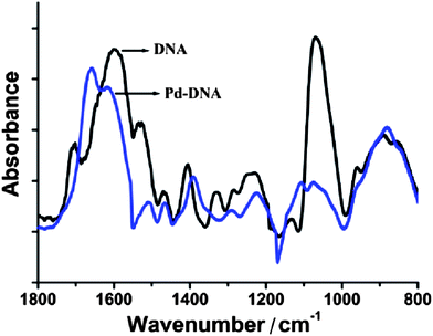 | ||
| Fig. 1 FTIR spectrum of Pd/DNA nanowires (blue) and FTIR spectrum of bare λ-DNA (black). 128 scans co-added and averaged, 4 cm−1 resolution. | ||
UV-Vis absorption spectra were employed to monitor the reduction of Pd(II) ions and the formation of metallic Pd(0) upon addition of the reducing agent. Electronic spectra of metal nanowires show absorption bands due to the excitation of the plasmon resonance. Noble metals that give a distinct plasmon peak, such as Au,56 Ag57 and Cu58 are relatively easy to examine by optical spectroscopy. For Pd, the overlap of the DNA and bands related to the reducing agent and Pd(II) complicates the spectra. Fig. 2 shows the UV-Vis absorption spectra of the Pd/DNA solution at different stages of the template synthesis process. The aqueous calf-thymus (CT-DNA) solution exhibits the characteristic nucleic acid absorption band at 260 nm (curve 1); upon complexation with Pd(II) ions, the dominant absorption maximum shifted to about 300 nm (curve 3). The formation of a Pd(II)-DNA complex was supported by the red-shift of the Pd(II) band to 400 nm from the value observed in aqueous PdCl42− of 390 nm (curve 2). After DMAB reduction to produce Pd metal, the 300 nm peak for the Pd(II)-DNA complex was narrowed, blue-shifted to 290 nm and the 400 nm Pd(II) peak disappeared. A long absorption tail, decreasing with wavelength in the range 300–600 nm, remains (curve 4). The shape of this absorption is consistent with metallic Pd nanostructures.59,60
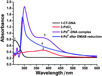 | ||
| Fig. 2 UV-Vis absorption spectra at different stages of the synthesis process: absorption spectra of CT-DNA (curve 1); aqueous K2PdCl4 solution (curve 2); the Pd(II)-DNA complex before DMAB treatment (curve 3) and the Pd/DNA solution after DMAB reduction (curve 4) showing the loss of the Pd(II) band near 400 nm. | ||
A high-resolution transmission electron microscopy (HRTEM) image and the EDS spectrum of a network of DNA/Pd nanowires is shown in Fig. 3. The EDS spectrum consisted mainly of Pd, C, Cu and P peaks. Cu peaks came from the carbon-coated Cu TEM grid, the Pd peak from nanowires, the C peak came from the TEM grid as well as DNA and the small P peak came from the DNA. The EDS analysis confirms directly the presence of Pd on the DNA template.
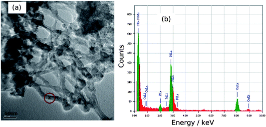 | ||
| Fig. 3 (a) HRTEM image of Pd/DNA nanowire network on a carbon-coated Cu grid and (b) the EDS spectrum at the point “x” in the image corresponding to a nanowire. | ||
Fig. 4 shows the X-ray powder diffraction pattern for a sample of Pd/DNA nanowires. Peaks due to reflections from the (111), (200), (220) and (311) planes of metallic Pd at 2θ values of 39°, 46°, 68° and 82° were observed; these are consistent with a previous report.59 The peaks are very broad and, upon fitting a pseudo-Voigt function to the most intense diffraction peak at 2θ = 39°, we estimate a crystallite diameter of 1.6 nm from the Scherrer equation. No peaks attributable to Pd oxides were observed, which rules out the presence of crystalline oxides.
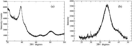 | ||
| Fig. 4 (a) X-ray diffraction pattern of Pd–DNA powder; the diffraction peaks originate from the (111), (200), (220) and (311) planes of metallic Pd at 2θ values of 39°, 46°, 68° and 82°. (b) pseudo-Voigt functions fitted to the peaks at 39° and 46°. The crystallite size was estimated using the Scherrer equation as 1.6 nm. | ||
XPS survey spectra indicated the presence of C, N, O, P (from the DNA template), Na (from the buffer or NaBH4 reductant) and Pd and Cl (from PdCl42−). Fig. 5 shows the Pd 3d spectrum. Peaks for both Pd(0) and Pd(II) oxidation states were observed. The doublet at 335.1 eV and 340.4 eV is assigned to Pd(0) and that at 336.4 eV and 341.7 eV to Pd(II) following previous reports.59,61 The feature at 346.3 eV is most likely a plasmon loss band associated with the peak at 335.1 eV. The plasmon energy of 11.2 eV is larger than the 7 eV expected for a surface plasmon and smaller than the bulk plasmon energy of 14 eV,62,63 but may be an effect of the small particle size. The Pd(II) state observed by XPS, but not XRD is interpreted as an amorphous oxyhydroxide coating the metal crystallite surfaces. We suggest this results from aquation of the PdCl42− followed by hydrolysis. PdCl42− is known to undergo exchange of Cl− ligands for H2O in non-complexing acidic solutions, the pH of λ-DNA is buffered at about 8, but some aquation of PdCl42− is still possible.64 Pd(OH2)42+ is unstable to hydrolysis at pH values above the pKa = 2.3.65
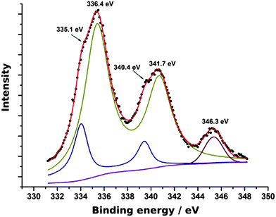 | ||
| Fig. 5 The Pd 3d XPS spectrum of Pd/DNA nanowires. The experimental data are the black symbols and the components making up the theoretical fit are shown as solid lines. | ||
3.2 Structural characterisation of Pd/DNA nanowires
Fig. 6 shows a selection of AFM images of the Pd/DNA nanowires aligned by molecular combing on Me3SiCl-treated Si/SiO2 substrates. Parallel Pd/DNA nanowires with diameters in the range 5–45 nm were observed. The height of bare λ-DNA, as measured by AFM, is well-known to be less than the crystallographic diameter of the double helix; values in the range 1–2 nm are typical. The nanowires appear smooth (Fig. 6a,b) and little Pd formed off the template is present. These AFM observations also revealed that the samples must be incubated at least 24 h before alignment in order to obtain smooth and continuous Pd nanowires over the whole length of λ-DNA. This was shown by imaging different samples which are aligned only a few hours after preparation and it was observed that in this case, the nanowires appeared with discontinuous parts along the DNA strands, as shown in Fig. 6d for the nanowires aligned after 2 h. The diameter distribution of the Pd/DNA nanowires was obtained by observing over 90 wires. Fig. 6c is a histogram of the average wire diameter 24 h after preparation. The average diameter of an individual wire was determined using section analysis along a 3 μm portion of the wire. The majority of the observed wires have diameters in the range 5–20 nm. It is clear that the Pd crystallite size determined by linewidth analysis of the XRD pattern is much less than the diameter of the nanowires, in contrast to the cases of Cu/DNA,17 Cu2O/DNA24 and Fe3O4/DNA nanowires26 where the AFM heights are comparable to the crystallite size from the Scherrer analysis. It is therefore also clear that the Pd metal does not form on the DNA template in the same way as previously studied systems, and a schematic illustration of the nanowire structure is presented in Fig. 7.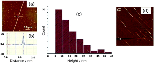 | ||
| Fig. 6 AFM images of Pd/DNA nanowires. (a) AFM image of a single Pd/DNA nanowire (scale bar = 1.5 μm); (b) Section of the nanowire in (a) at the indicated points showing the height difference between the Pd/DNA nanowire (≃23 nm) and the bare DNA strand (2 nm). (c) Height distribution of 90 Pd/DNA nanowires, the heights were determined from AFM images. (d) Discontinuous nanowires aligned after a reaction time of 2 h. The scale bar is 1 μm and the height (colour) scale is 30 nm. | ||
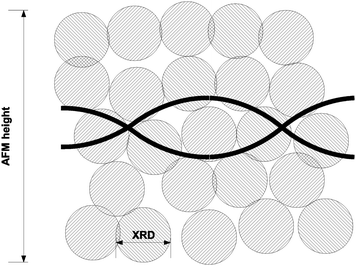 | ||
| Fig. 7 Schematic representation of the structure of the prepared DNA/Pd nanowires. The Pd crystallite size (≃1.6 nm) is substantially smaller than the nanowire heights observed by AFM (5–45 nm). | ||
In order to rationalise the AFM and XRD results, we carried out lattice gas simulations of the growth process. The initial configuration was assumed to be a series of spherical nuclei on the DNA template (Fig. 8a). The solid sites are shown in yellow (colour scale values > 1) and the solution sites are shown as purple-black (colour scale values < 1). The solution starts supersaturated with respect to the solid, i.e.,  where c is input to the simulation as a parameter, along with rate constants for dissolution and deposition of the solid, and c∞ is the concentration of dissolved metal ions at equilibrium. The parameter w determines the additional barrier to dissolution because a site has bonds to its nearest neighbours via eqn (1) and for deposition via eqn (2). This leads to the solid having a bulk surface tension which acts to minimize the area of its surface. The supersaturation can be related to the rate constants, after taking appropriate macroscopic averages, by
  . We therefore ran simulations with different values of k0diss, as defined in eqn (1), in order to study the effect of the driving force on the templating reaction. Unlike other materials we have studied, Pd deposition is expected to be much less reversible and therefore is modelled by choosing a larger driving force for deposition, i.e., a lower value for k0diss. Fig. 8b,d shows after 104 steps of the simulation the nuclei have grown; the growth is dominated by deposition of atoms at the step edges because of the large value of w chosen, and the crystallites are no longer spherical. When k0diss = 0.01 the crystallites are still separated from each other, but for k0diss = 0.1 there is already substantial overlap of neighbouring crystallites. As the growth continues, the overlap of neighbouring crystallites by dissolution and reprecipitation results in the appearance of a continuous nanowire (Fig. 8e) whose surface roughness has previously been modelled by a linear thermodynamic treatment.33 However, when k0diss = 0.01, events leading to the coalescence of neighbouring crystallites are rare and, though the external surface of the nanowire may appear very similar, there remain internal voids even at long simulation times. Such a simulation cannot model all the details of the actual Pd deposition, but it does indicate that when the deposition process is irreversible, a complex internal structure is a natural consequence. In the actual chemical system, additional features related to the presence of grain boundaries, deposition of oxide and the possibility of further nucleation events will naturally produce a granular morphology as in Fig. 7.
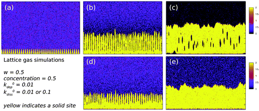 | ||
| Fig. 8 Lattice gas simulations of the growth of Pd/DNA nanowires on a square lattice of 2000 × 200 sites. The template lies along the x-axis in each figure. The common parameters are w = 0.5, concentration of dissolved metal ions, c = 0.5 (per site) and k0dep = 0.01. (a) t = 0; (b) k0diss = 0.01 and t = 104 time-steps; (c) k0diss = 0.01 and t = 107 time-steps; (d) k0diss = 0.1 and t = 104 time-steps and (e) k0diss = 0.1 and t = 107 time-steps. | ||
3.3 Electrical characterisation of Pd/DNA nanowires
The conductivity of the Pd/DNA nanowires was assessed qualitatively by the non-contact scanned conductance microscopy (SCM) technique. The measurement is performed via lift mode, a two-pass imaging technique in which the tip oscillates normal to the surface and a dc bias is applied between the tip and substrate. SCM is able to detect conductive objects resting on a dielectric film because of the change in the energy stored in the tip-substrate capacitance after insertion of a nanowire between the tip and the substrate; this change in energy is equivalent to a change in the force constant of the cantilever and therefore of the phase of the tip motion.66 Previous studies have revealed that conducting 1D structures such as single-wall carbon nanotubes have a negative phase shift with respect to background67 and insulating nanostructures such as polymers or λ-DNA show a positive phase shift.66,67 Fig. 9a–c shows a tapping mode AFM image and the corresponding scanned conductance images of Pd/DNA nanowires, when bias potentials of +6 V and −6 V were applied. The dark appearance of the nanowires in the phase images (Fig. 9b and c), which corresponds to a negative phase shift as the tip crosses the nanowire, and the quadratic variation of the phase shift with the bias voltage (Fig. 9d) are evidence that the nanowires are conductive and that the phase shift is not due to trapped charge effects. The thin, bright nanowires (positive phase shift) in the phase images are attributed to bare DNA strands because the height of these strands is in the range 1.5–2 nm. Moreover, the phase shift increases as the radius of the templated nanowires increases (Fig. 9e).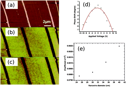 | ||
| Fig. 9 Electrical characterisation of Pd/DNA nanowires by scanned conductance microscopy. (a) AFM height image of Pd/DNA nanowires (the data scale is 25 nm). (b) and (c) the corresponding SCM phase images of the same nanowires with applied bias voltages of +6 V and −6 V respectively (the data scale is 3°). (d) Phase shift versus applied voltage for a single Pd/DNA nanowire (20 nm diameter) at a lift height of 60 nm aligned on 240 nm thick SiO2 on highly doped Si. (e) A quadratic was fitted to the plots of phase shift against bias voltage. The coefficients of V2 are plotted against the nanowire diameter at a constant lift height of 60 nm. | ||
It should be noted that, although the majority of the tested nanowires are conductive, the measurements also revealed the existence of non-conductive nanowires in the sample. These findings are consistent with the results of the XPS experiments which indicate the presence of oxide in the sample.
Quantitative measurements of Pd/DNA nanowire conductance were obtained by depositing nanowires on chemically oxidised Si(100) substrates to measure I–V curves using c-AFM following a previously developed method.4 The conductive AFM tip serves as one contact to a nanowire which protrudes from a dense network of nanowires to which an In/Ga eutectic is used to complete the circuit. Fig. 10 shows an SEM image of individual Pd/DNA nanowires stretched out from a dense mass of nanowires deposited from a dried droplet and the I–V curve of a single nanowire selected at the edge of such a dense mass. The dense mass of nanowires serves as the second contact to the nanowire. This technique allows the resistance of a single nanowire and the contacts to be separately determined; a series of I–V curves at different points on the nanowire are recorded and the resistance is then plotted as a function of distance along the nanowire. The conductivity is obtained from the slope of this plot and the measured height; the contact resistance is estimated by extrapolating the plot to zero distance.
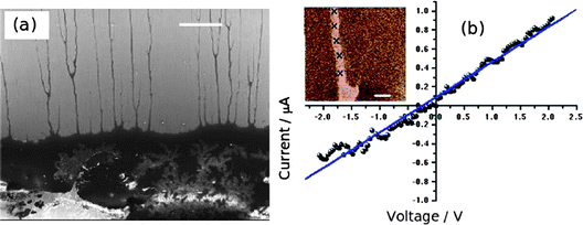 | ||
| Fig. 10 c-AFM measurements of Pd/DNA nanowires. (a) Electron micrograph of the dense mass of Pd/DNA nanowires (lower third of image); single Pd/DNA nanowires are seen protruding from the mass (scale bar = 20 μm). (b) Current–voltage curve with the tip contacting a single nanowire (inset = cAFM current image, data scale = 500 nA, tip/sample bias = 5 V, scale bar = 1 μm). | ||
Fig. 11 shows the plot of resistance against distance. The slope of the regression lines gives the nanowire resistance per unit length as (5.1 ± 0.2 × 10⁸ Ω cm−1). Using the diameter of the nanowire observed in the contact mode image (≃20 nm), the conductivity was determined as 1.6 × 10⁴ S m−1. This is the largest value of conductivity we observed for single Pd/DNA nanowires. This value is lower than both the bulk conductivity of Pd (9.5 × 10⁶ S m−1)68 and a previous report of a 50 nm diameter Pd/DNA nanowire of 2 × 10⁶ S m−1.14 A conductivity of 3.33 × 10⁵ S m−1 was also reported for a nanowire prepared by reduction of PdO (height 30 nm and length 450 nm61). The conductance of thin nanowires fabricated on DNA templates via Pd(II) reduction have also been reported; the average resistance of a single wire was 800 GΩ at 10 V.68 Our c-AFM measurements on various nanowires revealed resistance values in the range of 0.4–0.8 GΩ for the DNA/Pd nanowires prepared by the reduction of Pd(II) ions with DMAB and in the range of 2–8 MΩ for the nanowires prepared using NaBH4 as a reducing agent.
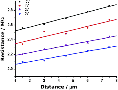 | ||
| Fig. 11 cAFM measurements of resistance at different points along a single Pd/DNA nanowire. The distance is that between the point at which the tip contacts the nanowire and the dense mass shown in Fig. 10. The nanowire resistance per unit length is the slope of the plot and the intercept at zero distance is the contact resistance. Measurements obtained at different setpoints (tip/sample force) are shown in different colours. | ||
Fig. 11 also shows the effect of increasing the tip/nanowire contact force by increasing the set point voltage from 0 to 3 V. A clear decrease in the intercept on the resistance axis is observed at higher forces, which is expected if the tip/nanowire junction is the dominant contact resistance. This is expected based on considerations of the area and previous estimates of the resistance at the second contact of 50–200 Ω.24 It is also clear that the contact resistance is very substantial and dominates the raw I–V data.
cAFM is inconvenient for temperature-dependent I–V measurement, therefore two-terminal Au microelectrode devices were fabricated in order to study this aspect. The DNA/Pd nanowires were transferred by the method of molecular combing onto clean Si/SiO2 substrates in the gap between microfabricated Au electrodes. In contrast to the case of polymer nanowires,4 the large contact resistance observed with Pd/DNA samples makes the I–V measurements of single Pd/DNA nanowires by two-terminal measurements difficult and non-linear characteristics were often observed (diode-like characteristics with a turn-on voltage of ≃0.6 V). Treatment of the single nanowires with reducing agents (gaseous hydrogen) did not reliably improve the behaviour. Instead we found that omitting the silanization of the SiO2 resulted in networks of Pd/DNA nanowires with consistent linear I–V characteristics (Fig. 12). Such nanowire networks have the advantage of having multiple routes for current flow within the nanowires and between the nanowire network and the contact pads. The networks exhibited linear I–V curves with measured currents in the nA range compared to the leakage current of the electrodes alone (≃100 fA). The conductance at zero bias increased with temperature over the range 233–373 K, which is opposite to the expected behaviour of a metal. However, similar observations68 have been made and attributed to a conduction mechanism based on the concept of a granular metal. Such behaviour seems natural given the mechanism of growth discussed above and the small grain size observed.
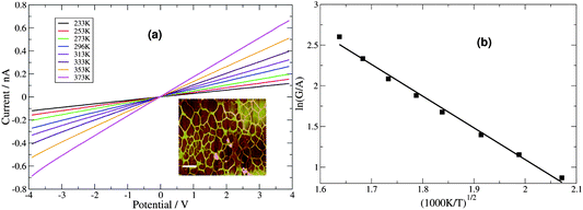 | ||
| Fig. 12 (a) Two-terminal microelectrode current–voltage curves for a network of Pd/DNA nanowires at temperatures from 233–373 K. (Inset: An AFM height image of the network, the data scale is 20 nm, scale bar = 500 nm). (b) The zero bias conductances, G, from (a) were divided by mean cross-sectional area, A, and ln(G/A) was plotted against T−1/2 to test the Efros–Shklovskii law. | ||
The single Pd/DNA nanowires also showed increased currents at higher temperatures; the linear portion of the data above the turn-on voltage could be used to make a plot of lnG versus 1/T from which an activation energy of 0.35 eV was derived, but the interpretation of this value is not straightforward. The zero bias conductance of the network was simpler to analyse and the behaviour for a granular metal under conditions where the grains are separated by a tunneling barrier was obtained (Fig. 12). The regression line shows the fit of the Efros–Shklovskii law,69,70 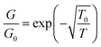 , to the data and T0 = 1850 ± 120 K or in terms of an energy, 0.16 ± 0.01 eV.
3.4 Hydrogen sensing with Pd/DNA nanowire networks
The more reliable electrical behaviour of the nanowire networks makes for a significantly more robust and resilient sensor than our single Pd/DNA nanowires. We have previously described the sensor performance in more detail,71 but give here a brief summary before discussing the modelling of the sensor response in terms of hydrogen diffusion in the nanowires. Fig. 13 shows the response of the resistance of the network to pulses of H2/N2 mixtures and pure N2 gas. The increase in resistance is caused by adsorption of H2 on the Pd surface dissociation to atomic hydrogen and in-diffusion to form the more resistive Pd hydride.72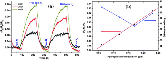 | ||
| Fig. 13 (a) Fractional change in network resistance to pulses of 1700 ppm H2 and pure N2 at temperatures from 330 K to 400 K. (b) Fractional change in resistance and response time against hydrogen concentration at 330 K. Response time is defined as the time to achieve 90% of the steady-state resistance change. | ||
The device signal, defined as  , is clearly reversible and the time for 90% of the signal to be achieved was about 85 s at 2300 ppm hydrogen. Recovery was slightly faster with a 90% recovery time of ≃60 s. The sensitivity is comparable to previous devices,47,50 although the response times are rather slow by comparison with electrodeposited Pd nanowires47 which have larger crystallite sizes. The maximum sensitivity of the sensor is increased from 0.09 to 0.26 with increasing temperature from 330 K to 400 K with good repeatability. Interestingly, this is in contrast to previous reports in which sensor response was observed to decrease with increasing temperature from 323 to 373 K,46 although it should be noted that it has recently been shown that even the sign of the response can change with temperature and that there may be competing effects such as hydride formation and swelling of the material in a single device.75
The response of the network to hydrogen was modelled as that of an ensemble of identical nanowires. The sorption of hydrogen in the nanowires was treated as a standard diffusion problem with cylindrical symmetry:
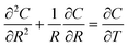 | (3) |
The boundary and initial conditions are C(1,T) = 1;  ; and C(R,0) = 0 for 0 ≤ R < 1. The dimensionless groups are defined as C = c(r)/c*; R = r/a and T = Dt/a2. D is the diffusion coefficient of hydrogen in the Pd/DNA nanowire, a is the radius of the nanowire and c* is the concentration of hydrogen at the nanowire surface. r is the radial coordinate and t is the time. The term
  vanishes for a nanowire which is uniform along its length. We also assume that the process is limited by diffusion in the cylindrical nanowire and not by any barrier at the surface. The radial variation of the dimensionless concentration is given by
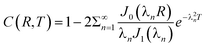 | (4) |
| σ(r) = ΔσHC(R) + σ0 | (5) |
The fractional change in conductance (G) of the nanowire can then be expressed in terms of the integral of 2πrσ in eqn (5) from R = 0 to R = 1:
 | (6) |
Substituting eqn (4) into eqn (6) gives the final result which can be used to model the data for conductance or resistance changes upon exposure to hydrogen:
 | (7) |
The system is linear, so the corresponding equation for the diffusion of hydrogen out of the nanowires upon exposure to nitrogen is simply:
 | (8) |
Eqn (7) and (8) were used as the regression models for the experimental data at each measured temperature (Fig. 14). The sums were truncated after λ20 which was found to give sufficient precision. We estimated the hydrogen atom diffusion coefficient in Pd/DNA at 330 K as 1.4 ± 0.1 × 10⁻¹⁴ cm2 s−1. This is much smaller than the reported diffusion coefficient in bulk Pd of 3.8 × 10⁻⁷ cm2 s−1 at room temperature37 and that obtained in a recent electrochemical study of 3.2 × 10⁻⁷ cm2 s−1.77 Previous reports also revealed that the hydrogen diffusion coefficient values in Pd thin films (50 nm to 1.34 μm thick) are 2–3 orders of magnitude smaller than of the bulk Pd at 298 K73 and in Pd thin films with thickness of 22.5 nm at 330 K which were reported as 6.9 × 10⁻¹¹ cm2 s−1.74 Other workers have studied H/D exchange in Pd using molecular beams; the exchange takes place on a timescale of order 10 s for 7 nm diameter Pd nanoparticles at 280 K.78 Our results are therefore not unprecedented for Pd nanostructures. The Pd/DNA nanowires here consist of small crystallites and therefore the low diffusion coefficient may be caused by grain boundary traps.74 We did observe a small difference between response and recovery, but with the recovery process slightly faster (Fig. 15). This suggests that diffusion is not the sole process limiting the response rate.
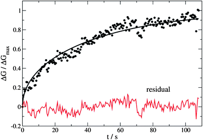 | ||
| Fig. 14 Change in nanowire conductance as a fraction of the steady-state value (ΔGmax). The temperature was 330 K, the mean nanowire radius was 20 nm and the hydrogen diffusion coefficient determined using eqn (7) as a regression model was 1.4 ± 0.1 × 10⁻¹⁴ cm2 s−1. | ||
![The change in diffusion coefficients obtained from the sensor response with increasing [H2] at 330 K.](/image/article/2013/FD/c3fd00017f/c3fd00017f-f15.gif) | ||
| Fig. 15 The change in diffusion coefficients obtained from the sensor response with increasing [H2] at 330 K. | ||
The diffusion coefficient is plotted as a function of hydrogen concentration at 330 K (Fig. 15). The results show that DH is roughly constant (∼1.4 × 10⁻¹⁴ cm2 s−1) over the range 600–1800 ppm but decreases to 0.85 × 10⁻¹⁴ cm2 s−1 when [H2] increased to 2300 ppm. This may indicate the onset of the α to β phase transition in Pd which has been reported to occur at concentrations of order 104 ppm.50
4 Conclusions
Pd/DNA nanowires formed by aqueous DNA-templating reactions have a substantially different structure to many other DNA-templated materials. A comparison of X-ray diffraction and AFM measurements shows that the apparently smooth wires observed in AFM comprise very small grains (1.6 nm) unlike Cu/DNA,17 Cu2O/DNA24 and Fe3O4/DNA nanowires,26 which have been shown to have a beads-on-a-string morphology in which the diameter of the wire matches the crystallite size estimated by diffraction. The nanowires are substantially less conductive than bulk Pd, but when prepared in the form of networks on Si/SiO2 substrates by molecular combing, they show stable I–V characteristics and their resistance increases in a reversible manner upon exposure to hydrogen gas. These networks exhibit response and recovery times of the order of 1 min and the fractional change in resistance was 26% at 400 K and 2300 ppm hydrogen. The hydrogen diffusivity estimated by modelling the sensor response was substantially smaller than the previous reported values for bulk Pd and thin films, which is likely due to grain boundary effects as a result of their granular nature. Nevertheless, these nanowire networks show comparable sensitivity to single Pd nanowire sensors and are very simple to fabricate.Acknowledgements
Dr Issa Al Amri from Sultan Qaboos University, Oman is thanked for help with the electron microscopy. ONE is thanked for funding research into nanowires at Newcastle.References
- Y. Ma, J. Zhang, G. Zhang and H. He, J. Am. Chem. Soc., 2004, 126, 7097–7101 CrossRef CAS.
- L. Dong, T. Hollis, S. Fishwick, B. A. Connolly, N. G. Wright, B. R. Horrocks and A. Houlton, Chem.–Eur. J., 2007, 13, 822 CrossRef CAS.
- J. Hannant, J. H. Hedley, J. Pate, A. Walli, S. A. Farha Al-Said, M. A. Galindo, B. A. Connolly, B. R. Horrocks, A. Houlton and A. R. Pike, Chem. Commun., 2010, 46, 5870 RSC.
- R. Hassanien, M. Al-Hinai, S. A. Farha Al-Said, R. Little, L. Šiller, N. G. Wright, A. Houlton and B. R. Horrocks, ACS Nano, 2010, 4, 2149 CrossRef CAS.
- S. M. D. Watson, J. H. Hedley, M. A. Galindo, S. A. Farha Al-Said, N. G. Wright, B. A. Connolly, B. R. Horrocks and A. Houlton, Chem.–Eur. J., 2012, 18, 12008 CrossRef CAS.
- P. Nickels, W. U. Dittmer, S. Beyer, J. P. Kotthaus and F. C. Simmel, Nanotechnology, 2004, 15, 1524 CrossRef CAS.
- S. A. F. Al-Said, R. Hassanien, J. Hannant, M. A. Galindo, S. Pruneanu, A. R. Pike, A. Houlton and B. R. Horrocks, Electrochem. Commun., 2009, 11, 550 CrossRef.
- S. Pruneanu, S. A. F. Al-Said, L. Q. Dong, T. Hollis, M. A. Galindo, N. G. Wright, A. Houlton and B. R. Horrocks, Adv. Funct. Mater., 2008, 18, 2444 CrossRef CAS.
- E. Braun, Y. Eichen, U. Sivan and G. Ben-Yoseph, Nature, 1998, 391, 775 CrossRef CAS.
- K. Keren, M. Krueger, R. Gilad, G. Ben-Yoseph, U. Sivan and E. Braun, Science, 2002, 297, 72 CrossRef CAS.
- K. Keren, R. S. Berman and E. Braun, Nano Lett., 2004, 4, 323 CrossRef CAS.
- W. E. Ford, O. Harnack, A. Yasuda and J. M. Wessels, Adv. Mater., 2001, 13, 1793 CrossRef CAS.
- J. Richter, R. Seidel, R. Kirsch, M. Mertig, W. Pompe, J. Plaschke and H. K. Schackert, Adv. Mater., 2000, 12, 507 CrossRef CAS.
- J. Richter, M. Mertig, W. Pompe, I. Mönch and H. K. Schackert, Appl. Phys. Lett., 2001, 78, 536 CrossRef CAS.
- Z. X. Deng and C. D. Mao, Nano Lett., 2003, 3, 1545 CrossRef CAS.
- C. F. Monson and A. T. Woolley, Nano Lett., 2003, 3, 359 CrossRef CAS.
- S. M. D. Watson, N. G. Wright, B. R. Horrocks and A. Houlton, Langmuir, 2010, 26, 2068 CrossRef CAS.
- E. Braun and K. Keren, Adv. Phys., 2004, 53, 441 CrossRef CAS.
- H. A. Becerril, R. M. Stolenberg, D. R. Wheeler, R. C. Davis, J. N. Harb and A. T. Woolley, J. Am. Chem. Soc., 2005, 127, 2828 CrossRef CAS.
- F. Patolsky, W. Weizmann, O. Liobasheveski and I. Willner, Angew. Chem., Int. Ed., 2002, 41, 2323 CrossRef CAS.
- T. Nishinaka, A. Takano, Y. Doi, M. Hashimoto, A. Nakamura, Y. Matsushita, J. Kumaki and E. Yashima, J. Am. Chem. Soc., 2005, 127, 8120 CrossRef CAS.
- H. Yan, S. H. Park, G. Finkelstein, J. H. Reif and T. H. LaBean, Science, 2003, 301, 1882 CrossRef CAS.
- H. Kudo and M. Fujihara, IEEE Trans. Nanotechnol., 2006, 5, 90 CrossRef.
- R. Hassanien, S. A. Farha Al-Said, L. Šiller, R. Little, N. G. Wright, A. Houlton and B. R. Horrocks, Nanotechnology, 2012, 23, 075601 CrossRef.
- D. Sarkar and M. Mandal, J. Phys. Chem. C, 2012, 116, 3227 CAS.
- H. D. A. Mohamed, S. M. D. Watson, B. R. Horrocks and A. Houlton, Nanoscale, 2012, 4, 5936 RSC.
- L. Dong, T. Hollis, B. A. Connolly, N. G. Wright, B. R. Horrocks and A. Houlton, Adv. Mater., 2007, 19, 1748 CrossRef CAS.
- W. U. Dittmer and F. C. Simmel, Appl. Phys. Lett., 2004, 85, 633 CrossRef CAS.
- L. Levina, V. Sukhovatkin, S. Musikhin, S. Cauchi, R. Nisman, D. P. Bazett-Jones and E. H. Sargent, Adv. Mater., 2005, 17, 1854 CrossRef CAS.
- J. L. Coffer, S. R. Bigham, R. F. Pinizzotto and H. Yang, Nanotechnology, 1992, 3, 69 CrossRef.
- D. S. Hopkins, D. Pekker, P. M. Goldbart and A. Bezryadin, Science, 2005, 308, 1762 CrossRef CAS.
- A. Houlton, A. R. Pike, M. A. Galindo and B. R. Horrocks, Chem. Commun., 2009, 1797 RSC.
- S. M. D. Watson, A. Houlton and B. R. Horrocks, Nanotechnology, 2012, 23, 505603 CrossRef.
- D. W. Keith and A. E. Farrell, Science, 2003, 301, 315 CrossRef CAS.
- R. Moy, Science, 2003, 301, 47 CrossRef CAS.
- M. Khanuja, S. Kala, B. R. Mehta and F. E. Kruis, Nanotechnology, 2009, 20, 015502 CrossRef.
- T. B. Flanagan and W. A. Oates, Annu. Rev. Mater. Sci., 1991, 21, 269 CrossRef CAS.
- J. S. Noh, J. M. Lee and W. Lee, Sensors, 2011, 11, 825 CrossRef CAS.
- E. Lee, J. M. Lee, J. H. Koo, W. Lee and T. Lee, Int. J. Hydrogen Energy, 2010, 35, 6984 CrossRef CAS.
- Y. Hu, D. Perello, U. Mushtaq and M. Yun, IEEE Trans. Nanotechnol., 2008, 7, 693 CrossRef.
- Y. Im, C. Lee, R. P. Vasquez, M. A. Banger, N. V. Myung, E. R. Menke, R. M. Penner and M. H. Yun, Small, 2006, 2, 356 CrossRef CAS.
- R. K. Joshi, S. Krishnan, M. Yoshimura and A. Kumar, Nanoscale Res. Lett., 2009, 4, 1191 CrossRef CAS.
- V. La Ferrara, B. Alfano, E. Massera and G. Di Francia, IEEE Trans. Nanotechnol., 2008, 7, 776 CrossRef.
- E. C. Walter, F. Favier and R. M. Penner, Anal. Chem., 2002, 74, 1546 CrossRef CAS.
- F. Yang, D. K. Taggart and R. M. Penner, Nano Lett., 2009, 9, 2177 CrossRef CAS.
- N. Tasaltin, S. Ozturk, N. Kilinç and Z. Ziya Ozturk, Appl. Phys. A: Mater. Sci. Process., 2009, 97, 745 CrossRef CAS.
- F. Yang, S. C. Kung, M. Cheng, J. C. Hemminger and R. M. Penner, ACS Nano, 2010, 4, 5233 CrossRef CAS.
- F. Favier, E. C. Walter, M. P. Zach, T. Benter and R. M. Penner, Science, 2001, 293, 2227 CrossRef CAS.
- S. Mubeen, T. Zhang, B. Yoo, M. A. Deshusses and N. V. Myung, J. Phys. Chem. C, 2007, 111, 6321 CAS.
- X. Q. Zeng, M. L. Latimer, Z. L. Xiao, S. Panuganti, U. Welp, W. K. Kwok and T. Xu, Nano Lett., 2011, 11, 262 CrossRef CAS.
- S. Yu, U. Welp, L. Z. Hua, A. Rydh, W. K. Kwok and H. H. Wang, Chem. Mater., 2005, 17, 3445 CrossRef CAS.
- K. J. Jeon, M. Jeun, E. Lee, J. M. Lee, K.-I. Lee, P. von Allmen and W. Lee, Nanotechnology, 2008, 19, 495501 CrossRef.
- D. Ding, Z. Chen and C. Lu, Sens. Actuators, B, 2006, 120, 182 CrossRef CAS.
- Y. Sun and H. H. Wang, Adv. Mater., 2007, 19, 2818 CrossRef CAS.
- G. B. Onoa, G. Cervantes, V. Moreno and M. J. Prieto, Nucleic Acids Res., 1998, 26, 1473 CrossRef CAS.
- H. Nakao, H. Shiigi, Y. Yamamot, S. Tokonami, T. Nagaoka, S. Sugiyama and T. Ohtani, Nano Lett., 2003, 3, 1391 CrossRef CAS.
- L. Berti, A. Alessandrini and P. Facci, J. Am. Chem. Soc., 2005, 127, 11216 CrossRef CAS.
- I. Lisiecki and M. P. Pileni, J. Phys. Chem., 1995, 99, 5077 CrossRef CAS.
- S. Kundu, K. Wang, D. Huitink and H. Liang, Langmuir, 2009, 25, 10146 CrossRef CAS.
- J. A. Creighton and D. G. Eadon, J. Chem. Soc. Faraday Trans., 1991, 104, 6767 Search PubMed.
- K. Nguyen, M. Monteverde, A. Filoramo, L. Goux-Capes, S. Lyonnais, P. Jegou, P. Viel, M. Goffman and J.-P. Bourgoin, Adv. Mater., 2008, 20, 1099 CrossRef CAS.
- V. D. Vankar and R. W. Vook, Surf. Sci., 1983, 131, 463 CrossRef CAS.
- P. Legare, Y. Holl and G. Maire, Solid State Commun., 1979, 31, 307 CrossRef CAS.
- L. I. Elding, Inorg. Chim. Acta, 1972, 6, 683 CrossRef CAS.
- B. I. Nabivanets and L. V. Kalabina, Russ. J. Inorg. Chem., 1970, 15, 818 Search PubMed.
- C. Staii, A. T. Johnson and N. J. Pinto, Nano Lett., 2004, 4, 859 CrossRef CAS.
- M. Bockrath, N. Markovic, A. Shepard, M. Tinkham, L. Gurevich, L. P. Kouwenhoven, M. W. Wu and L. L. Sohn, Nano Lett., 2002, 2, 187 CrossRef CAS.
- J. Lund, J. Dong, Z. Deng, C. Mao and B. A. Parviz, Nanotechnology, 2006, 17, 2752 CrossRef CAS.
- A. L. Efros and B. I. Shklovskii, J. Phys. C: Solid State Phys., 1975, 8, L49 CrossRef CAS.
- B. Abeles, P. Sheng, M. D. Coutts and Y. Arie, Adv. Phys., 1975, 24, 407 CrossRef CAS.
- M. N. Al-Hinai, N. G. Wright, A. B. Horsfall, R. Hassanien, B. R. Horrocks and A. Houlton, IEEE Sensors, 2011, 1 Search PubMed.
- B. D. Kay, C. H. F. Peden and D. W. Goodman, Phys. Rev. B, 1986, 34, 817 CrossRef CAS.
- H. Hagi, Mater. Trans., JIM, 1990, 31, 954 Search PubMed.
- Y. Li and Y. T. Cheng, Int. J. Hydrogen Energy, 1996, 21, 281 CrossRef CAS.
- D. Yang, L. Valentín, J. Carpena, W. Otaño, O. Resto and L. F. Fonseca, Small, 2013, 9, 188 CrossRef CAS.
- R. Smith and D. Otterson, J. Phys. Chem. Solids, 1970, 31, 187 CrossRef CAS.
- B. C. M. Martindale, D. Menshykau, S. Ernsta and R. G. Compton, Phys. Chem. Chem. Phys., 2013, 15, 1188 RSC.
- W. Ludwig, A. Savara, R. J. Madix, S. Schauermann and H.-J. Freund, J. Phys. Chem. C, 2012, 116, 3539 CAS.
Footnote |
| † Current address: Department of Engineering, Sohar College of Applied Science, Oman |
| This journal is © The Royal Society of Chemistry 2013 |