 Open Access Article
 This Open Access Article is licensed under a Creative Commons Attribution-Non Commercial 3.0 Unported Licence
One-step synthesis of Ni3S2 nanorod@Ni(OH)2nanosheet core–shell nanostructures on a three-dimensional graphene network for high-performance supercapacitors†
Weijia
Zhou‡
abd,
Xiehong
Cao‡
a,
Zhiyuan
Zeng
a,
Wenhui
Shi
a,
Yuanyuan
Zhu
a,
Qingyu
Yan
a,
Hong
Liu
*bc,
Jiyang
Wang
b and
Hua
Zhang
*a
aSchool of Materials Science and Engineering, Nanyang Technological University, 50 Nanyang Avenue, Singapore 639798, Singapore. E-mail: HZhang@ntu.edu.sg; Web: http://www.ntu.edu.sg/home/hzhang/
bState Key Laboratory of Crystal Materials, Center of Bio & Micro/nano Functional Materials, Shandong University, 27 Shandanan Road, Jinan 250100, China. E-mail: hongliu@sdu.edu.cn
cBeijing Institute of Nanoenergy and Nanosystems, Chinese Academy of Science, Beijing 100864, China
dNew Energy Research Institute, College of Environment and Energy, South China University of Technology, Guangzhou Higher Education Mega Centre, Guangzhou 510006, China
First published on 20th May 2013
Abstract
A three-dimensional graphene network (3DGN) grown on nickel foam is an excellent template for the synthesis of graphene-based composite electrodes for use in supercapacitors. Ni(OH)2nanosheets coated onto single-crystal Ni3S2nanorods grown on the surface of the 3DGN (referred to as the Ni3S2@Ni(OH)2/3DGN) are synthesized using a one-step hydrothermal reaction. SEM, TEM, XRD and Raman spectroscopy are used to investigate the morphological and structural evolution of the Ni3S2@Ni(OH)2/3DGN. Detailed electrochemical characterization shows that the Ni3S2@Ni(OH)2/3DGN exhibits high specific capacitance (1277 F g−1 at 2 mV s−1 and 1037.5 F g−1 at 5.1 A g−1) and areal capacitance (4.7 F cm−2 at 2 mV s−1 and 3.85 F cm−2 at 19.1 mA cm−2) with good cycling performance (99.1% capacitance retention after 2000 cycles).
Introduction
The increasing demand for energy and environmental protection has stimulated intensive research into energy storage and conversion from alternative energy sources. Currently, the supercapacitor is one of the most ideal candidates for green energy storage because of its high power density, super-high cycling life and safe operation.1–3 Based on the charge–storage mechanism, supercapacitors are generally divided into two types: electrical double-layer capacitors (EDLCs) that use carbon-active materials and pseudocapacitors that use redox-active materials. Among the numerous pseudocapacitor materials, transition metal oxides and hydroxides have been found to be excellent active materials, because of the variety of oxidation states they possess for charge transfer.4–8Nickel hydroxide is an especially attractive candidate for pseudocapacitors due to its layered structure, with large interlayer spacing and high theoretical specific capacitance.9–11 However, these types of pseudocapacitors are often confronted with a compromised rate capability and reversibility, which rely on the Faradic redox reaction. Recently, metal sulfides, another kind of active material, have attracted increasing interest due to their good performance in energy storage applications12–15 including supercapacitors.13,15Two-dimensional (2D) graphene has attracted much attention due to its high surface area, high flexibility and electrical conductivity.16–19Graphene and graphene-based materials are widely used in electrochemical applications,20 such as in graphene-based supercapacitors which have high specific capacitance.21–23 Since three-dimensional (3D) nanostructures with a short path for ion diffusion and large surface area provide more efficient contact between the ions of the electrolyte and the active materials, they are seen as promising electrode materials. For example, various 3D hybrid nanostructures, such as Co3O4@MnO2, CoO@NiHON and MnO2–NiO, have been used to significantly enhance both the capacitance and durability of supercapacitors.6,9,24
Recently, a novel 3D graphene network (3DGN) with an enlarged void volume, large surface area and high electrical conductivity was reported.25,26 Our previous work showed that the 3DGN grown on nickel foam is an excellent template for a graphene-based composite electrode, which opened up a promising new strategy for the application of graphene-based materials in supercapacitors.25,27 Herein, we report the growth of a novel 3D hybrid structure, i.e. a Ni3S2 nanorod@Ni(OH)2nanosheet core–shell nanostructure grown on a 3DGN on nickel foam, referred to as a Ni3S2@Ni(OH)2/3DGN, which has robust hierarchical porosity and a high specific surface area, using a simple one-step hydrothermal reaction. The composite and nanostructure of Ni3S2@Ni(OH)2/3DGN can be controlled by varying the reaction time and the mass ratio of Ni foam to thioacetamide (TAA). Electrochemical measurements of this novel hybrid structure exhibited a high capacitance and good cycling performance.
Experimental section
Growth of the Ni3S2@Ni(OH)2/3DGN hybrid structure
After the three-dimensional graphene network (3DGN) was grown on a nickel foam,25 Ni3S2@Ni(OH)2/3DGN heterostructures were prepared using a simple one-step hydrothermal process. In a typical experiment, a piece of 3DGN on nickel foam was wrapped in Teflon tape with exposure area of ∼1 cm2, and immersed into a Teflon-lined stainless steel autoclave containing a 20 mL homogeneous solution of 25 mg thioacetamide (TAA, C2H5NS). The autoclave was then sealed for and the hydrothermal reaction was conducted at 180 °C for 6, 12 and 24 h in order to obtain Ni3S2/3DGN, Ni3S2@Ni(OH)2/3DGN and Ni(OH)2/3DGN, respectively. After the autoclave was cooled down to room temperature, the samples were rinsed with a copious amount of distilled water and then dried in an electric oven at 60 °C for 12 h. As a control experiment, the nickel foam without 3DGN was used to synthesize a Ni3S2 nanorod@Ni(OH)2nanosheet/nickel foam heterostructure, referred to as Ni3S2@Ni(OH)2/Ni, at 180 °C for 12 h.Characterization
Field emission scanning electron microscopy (FESEM, Model JSM-7600F, JEOL Ltd., Tokyo, Japan) was used to characterize the morphologies of the synthesized samples. Transmission electron microscopy (TEM) images were taken using a JOEL JEM 2100F microscope. The chemical composition was investigated by using energy dispersive X-ray spectroscopy (EDX). The X-ray powder diffraction (XRD) pattern of each sample was recorded on a Bruke D8 Advance powder X-ray diffractometer using Cu Kα radiation (λ = 0.15406 nm). Raman spectra were collected with a WITEC CRM200 Raman System (488 nm laser, 2.54 eV, WITec, Germany).Electrochemical measurement
Cyclic voltammetry (CV) and galvanostatic charge–discharge were performed using a conventional three-electrode cell with 3 M KOH aqueous solution as the electrolyte and recorded on Solartron analytical equipment (Model 1470E, AMETEK, UK). The electrochemical impedance spectroscopy (EIS) test was performed using a conventional three-electrode system (CHI 660C, CH Instrument Inc., USA). The Ni3S2@Ni(OH)2/3DGN on Ni foam substrate (1 cm2), Ag/AgCl electrode (saturated KCl) and Pt wire were used as the working, reference and counter electrodes, respectively.Results and discussion
SEM images of the obtained Ni3S2@Ni(OH)2/3DGN (see the Experimental section for details) are shown in Fig. 1a–c. The 3DGN is covered by Ni3S2nanorods with a diameter of 0.5–1 μm and a length of 5–10 μm, which grew densely and almost vertically on the surface of the 3DGN. Magnified SEM images reveal that the Ni3S2nanorods are covered by Ni(OH)2nanosheets (Fig. 1c). With such a unique hierarchical structure, the space between the Ni3S2nanorods in the array can be efficiently utilized, allowing the electrolyte ions easier access to the surface of the active material. The XRDspectrum of the as-grown Ni3S2@Ni(OH)2/3DGN (Fig. 1d) shows peaks at 2θ = 21.7, 31.1, 37.8, 49.7 and 55.2°, which correspond to the single crystalline Ni3S2 (JCPDS no. 44-1418). It should be noted that two characteristic peaks for Ni at 2θ = 44.5 and 51.8° in the XRD pattern arise from the Ni foam substrate (JCPDS no. 65-2865). A very small amount of NiS (JCPDS no. 21-0041) is also observed in the XRD pattern. While the presence of the Ni(OH)2nanosheets was not confirmed by the XRD pattern, possibly due to there only being a tiny amount, it was confirmed from the HRTEM images and EDX (Fig. 2). | ||
| Fig. 1 (a) SEM image of Ni3S2@Ni(OH)2/3DGN (reaction time: 12 h). (b and c) The magnified SEM images of (a). (d) XRD pattern of Ni3S2@Ni(OH)2/3DGN. | ||
 | ||
| Fig. 2 (a) TEM image of Ni3S2@Ni(OH)2. (b and c) HRTEM images of Ni3S2nanorods and Ni(OH)2nanosheets from the white square areas highlighted in (a). (d) The corresponding SAED patterns of Ni3S2 and Ni(OH)2. (e and f) EDS spectrum and mapping results from a single hybrid nanostructure, conforming to the Ni3S2@Ni(OH)2 core–shell hierarchical structure. | ||
The nanostructures of the Ni(OH)2nanosheets and Ni3S2nanorods were further investigated using TEM. Fig. 2a shows the typical TEM image of an individual Ni3S2nanorod covered by thin Ni(OH)2nanosheets. The HRTEM image obtained from the white square area labelled (b) in Fig. 2a has a lattice spacing of 0.28 nm in the backbone area of the Ni3S2nanorod (Fig. 2b), which corresponds to the (110) interplanar spacing of Ni3S2 (hexagonal, a = b = 0.574 nm, c = 0.714 nm). The lattice distances of 0.27 and 0.23 nm in Fig. 2c correspond to the (011) and (100) faces of Ni(OH)2 (hexagonal, a = b = 0.312 nm, c = 0.46 nm). The corresponding selected-area electron diffraction (SAED) patterns (Fig. 2d) further confirmed the presence of the single crystalline Ni3S2nanorods and polycrystalline Ni(OH)2nanosheets. In addition, the energy dispersive X-ray spectrometry (EDS) analysis was conducted to confirm the composition of Ni3S2@Ni(OH)2 (Fig. 2e). The elements, Cu (from the copper TEM grid), Ni, S and O were all detected. The EDS mapping (Fig. 2f) clearly shows that the strongest signals for Ni and S were found in the backbone region, whereas only Ni and O signals were observed in the shell region, confirming the Ni3S2@Ni(OH)2 core–shell hierarchical structure.
Raman spectroscopy was used to further characterize the synthesized Ni3S2@Ni(OH)2/3DGN. Fig. 3 shows the typical G (∼1580 cm−1) and 2D (∼2732 cm−1) peaks that are characteristic of graphene in the 3DGN (curve a). The integrated peak area ratio of the 2D band to G band (∼0.51) indicates that the 3D graphene network contains few-layer graphene.25,26 The typical G (∼1563 cm−1) and 2D (∼2706 cm−1) peaks shown in curve b of Fig. 3 indicate that the graphene still existed after the synthesis of Ni3S2@Ni(OH)2 on the 3DGN. In order to further confirm the presence of graphene, the Ni2S3@Ni(OH)2 and Ni foam in Ni3S2@Ni(OH)2/3DGN were removed by immersing Ni3S2@Ni(OH)2/3DGN in a 1 M HCl aqueous solution at 60 °C overnight followed by rinsing with DI water several times. Fig. S1 (ESI†) indicates the 3DGN remained and 3D structure was still preserved, however some pores were observed on the surface of the graphene. In addition, two characteristic Raman peaks at ∼537.6 cm−1 (longitudinal optical, LO) and ∼1090.7 cm−1 (phonon modes, 2LO) were attributed to Ni(OH)2 in Ni3S2@Ni(OH)2/3DGN.28,29
 | ||
| Fig. 3 Raman spectra of (a) the 3DGN and (b) the Ni3S2@Ni(OH)2/3DGN. | ||
To investigate the morphological and structural evolution of the Ni3S2@Ni(OH)2/3DGN, a series of experiments with different hydrothermal reaction times were conducted (Fig. 4a–c), which indicate the evolution of the structure from Ni3S2nanorods to Ni3S2@Ni(OH)2, and then finally conversion to pure Ni(OH)2nanosheets. After a hydrothermal reaction time of 6 h, Ni3S2nanorods were obtained (Fig. 4a). The XRD pattern revealed that the nanorods were of the pure spinel Ni3S2 phase (Fig. 4d). However, if the hydrothermal reaction was carried out for 12 h, thin nanosheets were observed on the surface of the Ni3S2nanorods (Fig. 4b), which were confirmed to be Ni(OH)2 using TEM, SAED patterns and the EDS spectrum as shown in Fig. 2. The Ni(OH)2nanosheets are connected to each other, forming a highly porous morphology. At a longer reaction time of 24 h, structures composed of Ni(OH)2nanosheets were observed (Fig. 4c) and the Ni3S2nanorods had disappeared, which was also confirmed using TEM images (Fig. S2†). The absence of Ni3S2 peaks and the existence of Ni(OH)2 (JCPDS no. 14-0117) peaks at 2θ = 33, 38.5 and 59° in the XRD spectrum (Fig. 4d) further confirmed that the Ni3S2 was transformed to Ni(OH)2 after long reaction times (e.g. 24 h). Therefore, the Ni3S2nanorods can be used as a sacrificial template for synthesizing the Ni3S2@Ni(OH)2 hybrid structure using the hydrothermal reaction.
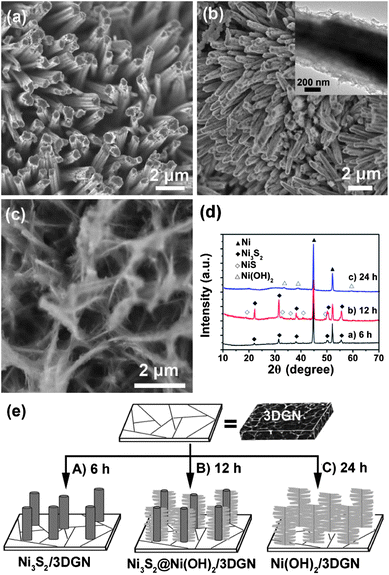 | ||
| Fig. 4 SEM images of the products obtained at different hydrothermal reaction times: (a) 6 h, (b) 12 h and (c) 24 h. Inset in (b): a magnified image of the Ni3S2@Ni(OH)2/3DGN structure. (d) The XRD patterns of the samples shown in (a–c). (e) Proposed mechanism for the growth of the Ni3S2@Ni(OH)2/3DGN structure. | ||
Based on the experimental results mentioned above, a possible growth mechanism for the Ni3S2@Ni(OH)2/3DGN is proposed (Fig. 4e). It has been reported that graphene oxide can be etched by hydrothermal steaming at 200 °C, forming porous structures.31 Therefore, we believe that the 3DGN can also be partially destroyed or etched during our hydrothermal process. In this case, some of the Ni foam could be exposed. Therefore, during the hydrothermal process, the active species (S ions) released from thioacetamide (TAA) react with the exposed Ni foam to form small Ni3S2 particles on the surface of the 3DGN after a reaction time of 2 h (Fig. S3a and b†). The morphology obtained is different from the original 3DGN (Fig. S3c†). At longer reaction times (e.g. 6 h), the Ni3S2nanorods grow on the surface of the 3DGN (step A in Fig. 4a and e). When the reaction time is increased to 12 h, the Ni3S2nanorods are hydrolyzed under the hydrothermal conditions and the Ni3S2 nanorod@Ni(OH)2nanosheet core–shell heterostructure is formed (step B in Fig. 4b and e). Finally, after a reaction time of 24 h, the Ni3S2nanorods are completely transformed into Ni(OH)2nanosheets (step C in Fig. 4c and e).
Fig. 5a shows the cyclic voltammogram (CV) curves of the Ni3S2@Ni(OH)2/3DGN, Ni3S2/3DGN, Ni(OH)2/3DGN and Ni3S2@Ni(OH)2/nickel foam (Ni3S2@Ni(OH)2/Ni) recorded at a scan rate of 5 mV s−1. All of the CV curves exhibit a pair of redox peaks, which are distinguishable from those of electric double-layer capacitors, implying the presence of a reversible Faradic reaction and pseudocapacitive behavior. The specific capacitance of the Ni3S2@Ni(OH)2/3DGN, Ni(OH)2/3DGN and Ni3S2/3DGN calculated from CV curves at 5 mV s−1 were 1125, 981 and 340 F g−1, respectively (for detailed calculations see the ESI†), which are higher than those of the composites directly grown on Ni foam without the 3DGN (i.e. Ni3S2@Ni(OH)2/Ni, Ni3S2/Ni and Ni(OH)2/Ni, Fig. S4†). This indicates that the 3DGN on the surface of the nickel foam plays an essential role in enhancing the supercapacitor performance. Importantly, the greatly enhanced electrochemical behavior of the Ni3S2@Ni(OH)2/3DGN, compared with the Ni(OH)2/3DGN and Ni3S2/3DGN, can be attributed to the synergistic effect resulting from the more active sites offered by the Ni(OH)2nanosheets and the quick electron transport of the highly crystalline Ni3S2nanorods.6,32
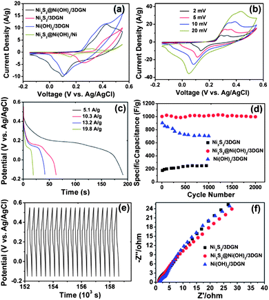 | ||
| Fig. 5 (a) Cyclic voltammograms of the Ni3S2@Ni(OH)2/3DGN, Ni3S2/3DGN, Ni(OH)2/3DGN and Ni3S2@Ni(OH)2/Ni foam electrodes within the potential range of −0.15 to 0.55 V at a constant scan rate of 5 mV s−1. (b) Cyclic voltammograms of the Ni3S2@Ni(OH)2/3DGN at different scan rates of 2, 5, 10 and 20 mV s−1. (c) Discharge curves for the Ni3S2@Ni(OH)2/3DGN at various current densities. (d) Cycling stability of the Ni3S2/3DGN, Ni3S2@Ni(OH)2/3DGN and Ni(OH)2/3DGN at a current density of 5.9 A g−1. (e) The last 20 charge–discharge curves for the Ni3S2@Ni(OH)2/3DGN. (f) Nyquist plots of the Ni3S2/3DGN, Ni3S2@Ni(OH)2/3DGN and Ni(OH)2/3DGN electrodes. | ||
Fig. 5b shows the CV curves of the Ni3S2@Ni(OH)2/3DGN at different scan rates. With the increase of scan rate, the current response increases accordingly and the shapes of CV curves are retained, indicating a good rate capability. The specific capacitance of the Ni3S2@Ni(OH)2/3DGN calculated from the CV curve is 1277 F g−1 at a scan rate of 2 mV s−1 and 716 F g−1 at a high scan rate of 20 mV s−1 (Fig. S5a†). Fig. 5c shows the galvanostatic discharge curves of the Ni3S2@Ni(OH)2/3DGN at different current densities. A high specific capacitance (1037.5 F g−1) was obtained at a discharge current density of 5.1 A g−1. Even at a relatively high current density of 19.8 A g−1, a specific capacitance of 398 F g−1 was obtained (Fig. S5b†). It should be noted that the aforementioned capacitance values of the composite electrodes (e.g. the Ni3S2@Ni(OH)2/3DGN and Ni3S2@Ni(OH)2/Ni) were calculated based on Ni3S2 (for detailed calculations, see the ESI†), since the exact mass ratio of Ni3S2 and Ni(OH)2 is difficult to determine. Therefore, the actual capacitance value of the Ni3S2@Ni(OH)2/3DGN structure should be higher than the aforementioned value, e.g. 1724 F g−1 at 2 mV s−1 and 1402 F g−1 at 5.1 A g−1 are the calculated values based on Ni(OH)2 (Fig. S5†).
The cycling performances of the Ni3S2@Ni(OH)2/3DGN, Ni(OH)2/3DGN and Ni3S2/3DGN at a current density of 5.9 A g−1 are shown in Fig. 5d. At this current density, the specific capacitance of 981 F g−1 (99.1% of the initial value of 1003 F g−1), calculated based on the pure Ni3S2, can be maintained after 2000 cycles. The shape of the last 20 charge–discharge curves (Fig. 5e) and the morphology of Ni3S2@Ni(OH)2 after 2000 cycles (Fig. S6†) are nearly unchanged, indicating the excellent cyclability of the Ni3S2@Ni(OH)2/3DGN electrode. However, the Ni3S2/3DGN shows a relatively low specific capacitance of 177 F g−1 for the first cycle. The specific capacitance increased slightly in subsequent cycles, possibly due to the formation of Ni(OH)2 on the surface of the Ni3S2nanorods while in the alkaline solution.33,34 While the Ni(OH)2/3DGN possesses a specific capacitance of 903 F g−1 for the first charge–discharge cycle, its specific capacitance decreases to 704 F g−1 (78% of the initial value) after 1000 cycles. The relatively worse cycling performance of Ni(OH)2 is similar to that seen in previous reports.29,30 Importantly, our Ni3S2@Ni(OH)2/3DGN electrode shows higher specific capacitance than many of the previously reported composite electrodes including CoO@NiHON (798.3 F g−1 at 1.67 A g−1, 95% maintained after 2000 cycles),9 NiS hollow sphere (927 F g−1 at 4.08 A g−1, 70% maintained after 3000 cycles)15 and NiO/3D graphene (745 F g−1 at 1.4 A g−1, 100% maintained after 2000 cycles)25 electrodes. In addition, electrochemical impedance spectroscopy (EIS) was also employed to characterize the composite electrodes (Fig. 5f). The equivalent series resistance (ESR) values of the Ni3S2/3DGN, Ni3S2@Ni(OH)2/3DGN and Ni(OH)2/3DGN are 1.07, 1.13 and 1.33 Ω, respectively, which are smaller than that reported for Ni(OH)2-coated nickel foam electrodes with high capacitive performance.35 Compared to the aforementioned 3DGN-based composites, Ni3S2@Ni(OH)2/Ni has a higher ESR value (4.57 Ω), indicating that the 3DGN improved the charge transport properties of the composite electrodes (Fig. S4d†).
Fabrication of electrodes with high mass loading of active materials has practical significance in supercapacitor devices.36,37 However, the increase in loading density often results in a decrease of the performance of these electrochemical devices.38 Fortunately, our Ni3S2@Ni(OH)2/3DGN electrode with a high loading density (∼3.7 mg cm−2) still exhibits excellent supercapacitor performance as mentioned above. Moreover, the high areal capacitance of the Ni3S2@Ni(OH)2/3DGN is 4.7 F cm−2 at 2 mV s−1 and 3.85 F cm−2 at 19.1 mA cm−2 (Fig. S5†), which is much better than the reported values for materials based on Co3O4@MnO2 (0.56 F cm−2 at 11.25 mA cm−2),6 MnO2/carbon nanotubes (2.8 F cm−2 at 0.05 mV s−1)38 and Co3O4/NiO (2.56 F cm−2 at 2 A g−1).39 To further evaluate the performance of the Ni3S2@Ni(OH)2/3DGN electrode, the energy density (E) and power density (P) were calculated from the charge–discharge curves (see the ESI† for the details). The Ni3S2@Ni(OH)2/3DGN gave a high energy density of 70.6 Wh kg−1 at a power density of 1.3 kW kg−1, and still retains a value of 27.1 Wh kg−1 at a power density of 5 kW kg−1 (Fig. S7†).
The aforementioned results reveal the high specific capacitance, remarkable rate capability as well as excellent cycling performance of the Ni3S2@Ni(OH)2/3DGN when used as high-performance electrochemical pseudocapacitors. Such superior performance of the Ni3S2@Ni(OH)2/3DGN can be attributed to the following factors. First, the CVD grown 3DGN on nickel foam with a high surface area and high electrical conductivity can effectively collect and transfer charges.25,27 Second, the Ni(OH)2nanosheets possess a high contact area with the electrolyte, thus enabling fast and reversible redox reactions, which improve the specific capacitance.9,35 Third, the single-crystal Ni3S2nanorod array grown on the surface of the 3DGN provides large open spaces and a shorter ion diffusion path, which avoid the use of a polymer binder or conductive additive in the electrode materials.6,40 Importantly, Ni3S2 has a heazlewoodite structure with short metal–metal distances in an approximately body-centred cubic sulphur lattice, which results in it having good electrical properties33 and enables the quick transport of electrons along the Ni3S2nanorods. In addition, the one-step synthesized Ni3S2@Ni(OH)2 core–shell nanostructures on the 3DGN aids the electron transfer between the Ni(OH)2, Ni3S2 and 3DGN components due to the perfect interface connection between them.
Conclusions
In summary, the large-amount Ni3S2@Ni(OH)2/3DGN, i.e. Ni(OH)2nanosheets coated on the single-crystal Ni3S2nanorods grown on the surface of 3D graphene network, is synthesized by a simple one-step hydrothermal reaction. By controlling the reaction time, different composites and nanostructures, i.e., Ni3S2/3DGN, Ni3S2@Ni(OH)2/3DGN and Ni(OH)2/3DGN, are obtained. Detailed electrochemical characterization shows that the Ni3S2@Ni(OH)2/3DGN exhibits high specific capacitance (1277 F g−1 at 2 mV s−1 and 1037.5 F g−1 at 5.1 A g−1) and areal capacitance (4.7 F cm−2 at 2 mV s−1 and 3.85 F cm−2 at 19.1 mA cm−2) with good cycling performance (99.1% capacitance retention after 2000 cycles). The enhanced supercapacitor performance might arise from the synergistic effect between the Ni(OH)2nanosheets, Ni3S2nanorods and 3D graphene network.Acknowledgements
This work was supported by MOE under AcRF Tier 2 (ARC 10/10, no. MOE2010-T2-1-060) and AcRF Tier 1 (2012-T1-001-161), Start-Up Grant (M4080865.070.706022) in NTU. This research is also funded by the Singapore National Research Foundation and the publication is supported under the Campus for Research Excellence And Technological Enterprise (CREATE) programme. H. L. thanks the support from the NSFDYS: 50925205 in Shandong University in China, the National Natural Science Foundation of China (NSFDYS: 50925205), and the "100 Talents Program" of Chinese Academy of Sciences.Notes and references
- J. R. Miller and P. Simon, Science, 2008, 321, 651 CrossRef CAS.
- P. Simon and Y. Gogotsi, Nat. Mater., 2008, 7, 845 CrossRef CAS.
- J. Jiang, J. P. Liu, W. W. Zhou, J. H. Zhu, X. T. Huang, X. Y. Qi, H. Zhang and T. Yu, Energy Environ. Sci., 2011, 4, 5000 CAS.
- S. Chen, J. W. Zhu, X. D. Wu, Q. F. Han and X. Wang, ACS Nano, 2010, 4, 2822 CrossRef CAS.
- K. Xie, J. Li, Y. Q. Lai, W. Lu, Z. Zhang, Y. X. Liu, L. Zhou and H. T. Huang, Electrochem. Commun., 2011, 13, 657 CrossRef CAS.
- J. P. Liu, J. Jiang, C. W. Cheng, H. X. Li, J. X. Zhang, H. Gong and H. J. Fan, Adv. Mater., 2011, 23, 2076 CrossRef CAS.
- H. L. Wang, H. S. Casalongue, Y. Y. Liang and H. J. Dai, J. Am. Chem. Soc., 2010, 132, 7472 CrossRef CAS.
- C. C. Hu, K. H. Chang, M. C. Lin and Y. T. Wu, Nano Lett., 2006, 6, 2690 CrossRef CAS.
- C. Guan, J. P. Liu, C. W. Cheng, H. X. Li, X. L. Li, W. W. Zhou, H. Zhang and H. J. Fan, Energy Environ. Sci., 2011, 4, 4496 CAS.
- F. S. Cai, G. Y. Zhang, J. Chen, X. L. Gou, H. K. Liu and S. X. Dou, Angew. Chem., Int. Ed., 2004, 43, 4212 CrossRef CAS.
- S. B. Yang, X. L. Wu, C. L. Chen, H. L. Dong, W. P. Hu and X. K. Wang, Chem. Commun., 2012, 48, 2773 RSC.
- Y. P. Du, Z. Y. Yin, J. X. Zhu, X. Huang, X. J. Wu, Z. Y. Zeng, Q. Y. Yan and H. Zhang, Nat. Commun., 2012, 3, 1177 CrossRef.
- F. Tao, Y. Q. Zhao, G. Q. Zhang and H. L. Li, Electrochem. Commun., 2007, 9, 1282 CrossRef CAS.
- S. J. Bao, C. M. Li, C. X. Guo and Y. Qiao, J. Power Sources, 2006, 159, 287 CrossRef.
- T. Zhu, Z. Y. Wang, S. J. Ding, J. S. Chen and X. W. Lou, RSC Adv., 2011, 1, 397 RSC.
- W. S. Hummers and R. E. Offeman, J. Am. Chem. Soc., 1958, 80, 1339 CrossRef CAS.
- S. Stankovich, D. A. Dikin, G. H. B. Dommett, K. M. Kohlhaas, E. J. Zimney, E. A. Stach, R. D. Piner, S. T. Nguyen and R. S. Ruoff, Nature, 2006, 442, 282 CrossRef CAS.
- X. Huang, X. Y. Qi, F. Boey and H. Zhang, Chem. Soc. Rev., 2012, 41, 666 RSC.
- X. Huang, Z. Y. Yin, S. X. Wu, X. Y. Qi, Q. Y. He, Q. C. Zhang, Q. Y. Yan, F. Boey and H. Zhang, Small, 2011, 7, 1876 CrossRef CAS.
- (a) S. X. Wu, Q. Y. He, C. L. Tan, Y. D. Wang and H. Zhang, Small, 2013, 9, 1160 CrossRef CAS; (b) K. Chang and W. X. Chen, ACS Nano, 2011, 5, 4720 CrossRef CAS.
- Y. W. Zhu, S. Murali, M. D. Stoller, K. J. Ganesh, W. W. Cai, P. J. Ferreira, A. Pirkle, R. M. Wallace, K. A. Cychosz, M. Thommes, D. Su, E. A. Stach and R. S. Ruoff, Science, 2011, 332, 1537 CrossRef CAS.
- M. D. Stoller, S. Park, Y. W. Zhu, J. An and R. S. Ruoff, Nano Lett., 2008, 8, 3498 CrossRef CAS.
- G. H. Yu, L. B. Hu, N. Liu, H. L. Wang, M. Vosgueritchian, Y. Yang, Y. Cui and Z. N. Bao, Nano Lett., 2011, 11, 4438 CrossRef CAS.
- J. P. Liu, J. Jiang, M. Bosmanc and H. J. Fan, J. Mater. Chem., 2012, 22, 2419 RSC.
- X. H. Cao, Y. M. Shi, W. H. Shi, G. Lu, X. Huang, Q. Y. Yan, Q. C. Zhang and H. Zhang, Small, 2011, 7, 3163 CrossRef CAS.
- Z. P. Chen, W. C. Ren, L. B. Gao, B. L. Liu, S. F. Pei and H. M. Cheng, Nat. Mater., 2011, 10, 424 CrossRef CAS.
- X. C. Dong, H. Xu, X. W. Wang, Y. X. Huang, M. B. C. Park, H. Zhang, L. H. Wang, W. Huang and P. Chen, ACS Nano, 2012, 6, 3206 CrossRef CAS.
- G. D. Zhou, D. W. Wang, L. C. Yin, N. Li, F. Li and H. M. Cheng, ACS Nano, 2012, 6, 3214 CrossRef CAS.
- J. Yan, W. Sun, T. Wei, Q. Zhang, Z. J. Fan and F. Wei, J. Mater. Chem., 2012, 22, 11494 RSC.
- B. Zhao, J. S. Song, P. Liu, W. W. Xu, T. Fang, Z. Jiao, H. J. Zhang and Y. Jiang, J. Mater. Chem., 2011, 21, 18792 RSC.
- T. H. Han, Y. K. Huang, A. T. L. Tan, V. P. Dravid and J. X. Huang, J. Am. Chem. Soc., 2011, 133, 15264 CrossRef CAS.
- C. H. Lai, K. W. Huang, J. H. Cheng, C. Y. Lee, W. F. Lee, C. T. Huang, B. J. Hwang and L. J. Chen, J. Mater. Chem., 2009, 19, 7277 RSC.
- A. N. Buckley and R. Woods, J. Appl. Electrochem., 1991, 21, 575 CrossRef CAS.
- B. Zhang, X. C. Ye, W. Dai, W. Y. Hou and Y. Xie, Chem.–Eur. J., 2006, 12, 2337 CrossRef CAS.
- G. W. Yang, C. L. Xu and H. L. Li, Chem. Commun., 2008, 6537 RSC.
- M. D. Stoller and R. S. Ruoff, Energy Environ. Sci., 2010, 3, 1294 CAS.
- G. H. Yu, L. B. Hu, M. Vosgueritchian, H. L. Wang, X. Xie, J. R. McDonough, X. Cui, Y. Cui and Z. N. Bao, Nano Lett., 2011, 11, 2905 CrossRef CAS.
- L. B. Hu, W. Chen, X. Xie, N. Liu, Y. Yang, H. Wu, Y. Yao, M. Pasta, H. N. Alshareef and Y. Cui, ACS Nano, 2011, 5, 8904 CrossRef CAS.
- X. H. Xia, J. P. Tu, Y. Q. Zhang, X. L. Wang, C. D. Gu, X. B. Zhao and H. J. Fan, ACS Nano, 2012, 6, 5531 CrossRef CAS.
- Y. G. Li, B. Tan and Y. Y. Wu, Nano Lett., 2008, 8, 265–270 CrossRef CAS.
Footnotes |
| † Electronic supplementary information (ESI) available: Calculation methods for the specific capacitance and areal capacitance of the composite electrodes prepared, photos and SEM images of the Ni3S2@Ni(OH)2/3DGN after the removal of Ni3S2@Ni(OH)2 and Ni foam, TEM images of the Ni(OH)2nanosheets and Ni3S2@Ni(OH)2 after cycling, SEM images of the untreated 3DGN and Ni3S2@Ni(OH)2/Ni, electrochemical characterizations of Ni3S2/Ni, Ni3S2@Ni(OH)2/Ni and Ni(OH)2/Ni, the calculated specific capacitance and areal capacitance data for the Ni3S2@Ni(OH)2/3DGN, and the Ragone plot of energy density (E) versus power density (P) of the Ni3S2@Ni(OH)2/3DGN electrode are provided in Fig. S1–S7. See DOI: 10.1039/c3ee40155c |
| ‡ These authors contributed equally to this work. |
| This journal is © The Royal Society of Chemistry 2013 |