 Open Access Article
 This Open Access Article is licensed under a
 Creative Commons Attribution 3.0 Unported Licence
Ultrathin amorphous zinc-tin-oxide buffer layer for enhancing heterojunction interface quality in metal-oxide solar cells†
Yun Seog
Lee‡
a,
Jaeyeong
Heo‡
bc,
Sin Cheng
Siah
a,
Jonathan P.
Mailoa
a,
Riley E.
Brandt
a,
Sang Bok
Kim
b,
Roy G.
Gordon
b and
Tonio
Buonassisi
*a
aMassachusetts Institute of Technology, Cambridge, MA 02139, USA. E-mail: buonassisi@mit.edu
bDepartment of Chemistry and Chemical Biology, Harvard University, Cambridge, MA 02138, USA
cDepartment of Materials Science and Engineering, Chonnam National University, Gwangju 500-757, Korea
First published on 15th April 2013
Abstract
We demonstrate a tunable electron-blocking layer to enhance the performance of an Earth-abundant metal-oxide solar-cell material. A 5 nm thick amorphous ternary metal-oxide buffer layer reduces interface recombination, resulting in sizable open-circuit voltage and efficiency enhancements. This work emphasizes the importance of interface engineering in improving the performance of Earth-abundant solar cells.
Broader contextThin film solar cells comprising Earth-abundant elements are promising candidates for renewable energy applications due to their sustainable raw-material usage and potential for cost-effective manufacturing. Earth-abundant metal-oxide semiconductors comprise an attractive set of materials for photovoltaic applications, given their auspicious optoelectronic properties and chemical stability suitable for transparent conductor, light-absorber, and transparent buffer layers. For instance, cuprous oxide (Cu2O) and zinc oxide (ZnO) form a type-II heterojunction, yet thin film solar cells of this composition often exhibit substantial power conversion efficiency losses deriving from low open-circuit voltage and fill-factor, believed to be caused by junction non-idealities. In this study, a conformal nanometer-scale amorphous zinc tin oxide buffer layer is introduced between the Cu2O absorber and the aluminum-doped ZnO transparent conductor, reducing dark saturation current density by over an order of magnitude, and improving the open-circuit voltage to 0.553 V and power conversion efficiency to 2.65%. Atomic layer deposition enables precise tunability of buffer layer stoichiometry and conformity to textured surfaces. This amorphous electron-blocking layer approach may be extended to improve the interface quality in other Earth-abundant thin film materials. |
Thin film solar cells comprising Earth-abundant, non-toxic, and air-stable materials represent a promising class of photovoltaic (PV) devices compatible with terawatts-scale deployment.1–3 Cuprous oxide (Cu2O) is one of several candidate materials under consideration with the potential to reach 20% power conversion efficiency.4,5 Doping this material to make it n-type has proven to be challenging, thus a common PV device architecture comprises a Cu2O–ZnO heterojunction structure. However, device efficiencies remain low, with wafer-based Cu2O devices (by thermal oxidation of Cu sheets at ∼1010 °C) reaching 4.1% (ref. 6) and thin film Cu2O devices (by electrochemical deposition) reaching 1.3% (ref. 7). The open-circuit voltage (VOC) of these devices is significantly below the theoretical limit of Cu2O, due to a low built-in potential caused by non-ideal band alignment between the absorber and transparent conducting oxide (TCO), and a high recombination-current driven by interface-traps.8,9
To mitigate the latter voltage-loss mechanism, we introduce a thin (∼5 nm) buffer layer between the absorber and the TCO. This layer serves as an electron-blocking layer, reducing the magnitude of the recombination current at the absorber–TCO interface. This approach is reminiscent of the Si-based heterojunction with intrinsic thin layer (HIT) devices, which exhibit VOC superior to the best Si homojunction devices by creating a small energy barrier with a low density of interface-traps.10 This energy barrier is expressed as a conduction-band offset (ΔECB) of the buffer layer relative to the absorber layer; ΔECB must be carefully “tuned” to avoid current losses (stemming from too high ΔECB) or voltage losses (stemming from a negative ΔECB).11 This tunability can be achieved by using ternary compounds for the buffer layer, whereby the ratio of two cations (anions) typically modifies the conduction (valence) band position.12,13 Judicious composition selection of this ternary compound allows one to simultaneously limit the concentrations of carriers at the interface as well as reduce the interface-trap density, which reduces dark saturation current density (J0) and increases VOC. To achieve maximum benefit, this layer needs to be thin enough to avoid significant optical absorption (current loss) or resistive loss.
In this study, we introduce an ultrathin amorphous zinc tin oxide (a-ZTO) film as an electron-blocking layer to inhibit recombination at the interface between the Cu2O absorber and the Al-doped ZnO (AZO) TCO. Amorphous metal oxides are a new class of semiconductors recently highlighted in transparent electronics due to their superior electronic transport properties with high optical transparency.14,15 Specifically, a-ZTO is a non-toxic and scalable material (high elemental abundance), and has shown a field-effect mobility of up to 13 cm2 V−1 s−1 with good thermal stability.16 Recently, ZTO has shown potential as a Cd-free buffer layer for CIGS solar cells exhibiting performance comparable to devices with CdS buffer layers.17 By controlling the atomic composition of the a-ZTO films, we show that the optical and electrical properties of the buffer layer can be tuned and the heterojunction interface quality can be improved. We demonstrate a power conversion efficiency of our thin film Cu2O devices of 2.65% (total area) with an optimized buffer layer, which to our knowledge is the highest efficiency reported so far for solid-state thin film solar cells with electrochemically deposited Cu2O.
We fabricate Cu2O-based thin film solar cells in the substrate configuration with ultrathin a-ZTO (or ZnO) buffer layers. Fig. 1 shows the device architecture and corresponding electron microscopy images of these devices. 2.5 µm Cu2O thin films are deposited by an electrochemical method on patterned Au electrodes. Grains in the Cu2O films have (111) preferred orientation when deposited by lactate solution, which results in a highly textured top surface morphology (Fig. 1b) exhibiting reduced optical reflection desirable for photovoltaic applications.18 A 5 nm thick a-ZTO buffer layer and an 80 nm thick AZO layer are sequentially deposited by ALD at 120 °C. Cross-sectional images of the solar cells taken with high-resolution transmission electron microscopy (HR-TEM) show the individual layers clearly (Fig. 1d). The amorphous nature of the ZTO buffer layer is observed in contrast to crystalline Cu2O and AZO layers. It is confirmed that the ALD process enables a highly conformal coverage of a-ZTO and AZO films on the textured Cu2O surfaces without pin-holes (Fig. 1c and d). The AZO films exhibit an electrical resistivity of 5.9 × 10⁻³ Ω cm. Al grids that shadow ∼4% of the device surface area are deposited for top-side electrodes. As a control, a baseline device containing an undoped ZnO (instead of a-ZTO) buffer layer grown by ALD at 120 °C with the same thickness (5 nm) is also fabricated.
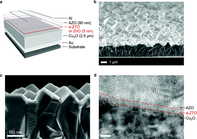 | ||
| Fig. 1 (a) A schematic of the structure of the substrate type Cu2O-based solar cells with a-ZTO (or ZnO for the “control” device) buffer layers. (b) Cross-sectional scanning electron microscopy (SEM) image of the device, exhibiting a highly textured top surface stemming from (111) preferred growth of Cu2O. (c) Magnified SEM image near the junction interface. Conformal coating of a-ZTO and AZO layers is demonstrated. (d) HR-TEM image near the junction interface. Dashed lines indicate phase boundaries between the amorphous ZTO layer (Zn/Sn = 1/0.27) and surrounding crystalline Cu2O and AZO layers. | ||
A cyclic amide of tin ((1,3-bis(1,1-dimethylethyl)-4,5-dimethyl-(4R,5R)-1,3,2-diazastannolidin-2-ylidene)Sn(II)) as the Sn precursor and diethyl zinc as the Zn precursor enables the low-temperature ALD of a-ZTO thin films.16,19 The atomic composition of the a-ZTO buffer layer is varied by choosing the ratio of ALD sub-cycles for ZnO and SnO2 deposition to be 3/1, 1/1 or 1/3. Atomic concentrations of Zn, Sn, and O in the films are measured by Rutherford backscattering spectroscopy (RBS). Fig. 2a shows the RBS spectra for three different a-ZTO films with different ZnO-to-SnO2 sub-cycle ratios, grown on glassy carbon substrates pre-treated by UV-ozone. No obvious peaks except for Zn, Sn, and O from the films and C from the substrate are observed. The Zn-to-Sn ratio is measured to be 1/0.27, 1/0.59, and 1/1.8 for the films with ZnO-to-SnO2 sub-cycle ratios of 3/1, 1/1, and 1/3, respectively. Oxygen concentrations are 13–19% higher than the values calculated assuming stoichiometric ZnO and SnO2. A similar oxygen-rich composition is observed for pure SnO2 ALD using hydrogen peroxide (H2O2) as the oxidant.19 The microstructure of the buffer layers is evaluated by glancing-angle X-ray diffraction (GAXRD) as shown in Fig. 2b. Diffraction peaks from the undoped ZnO film indicate crystalline hexagonal ZnO. On the other hand, all ZTO films are amorphous consistent with HR-TEM measurements. Broad peaks at around 34° are observed for the three ZTO films, which is characteristic of a-ZTO.16,20 The amorphous nature of these films is a likely consequence of the different cation valences and crystal structures of each pure binary metal oxide; the crystal structures of ZnO and SnO2 are wurtzite and rutile, respectively.21,22
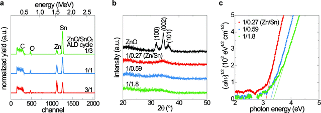 | ||
| Fig. 2 (a) RBS spectra of the a-ZTO films with three different ZnO-to-SnO2 sub-cycle ratios. The carbon signal arises from the glassy carbon substrates used for the measurements. (b) GAXRD spectra of the ZTO films. ZnO is included as a reference. All ZTO films lack distinct diffraction peaks, indicating their amorphous nature. (c) Bandgap extraction from the plot of (αhν)1/2 as a function of photon energy. | ||
Optical and electrical properties of the a-ZTO films are tuned by varying the Zn-to-Sn ratio. All films exhibit high transmittance in the visible wavelength range and higher transmittance than undoped ZnO in the UV range (Fig. S1†). The Tauc model is typically used to determine fundamental bandgap values for amorphous semiconductors.23,24 The bandgaps of a-ZTO films are determined from the plot of (αhν)1/2 as a function of photon energy shown in Fig. 2c. As the Zn-to-Sn ratio of the film decreases from 1/0.27 to 1/1.8, the bandgap gradually increases from 3.12 to 3.37 eV. Hall measurements reveal an n-type conductivity with an electron density of 3.5 × 1016 cm−3 and a mobility of 3.7 cm2 V−1 s−1 for the a-ZTO film with a Zn-to-Sn ratio of 1/0.27, while the other a-ZTO films with higher Sn contents exhibit resistivities larger than 2 × 10³ Ω cm and Hall voltages too small to measure, due to a decrease of carrier concentration.16 Low carrier concentrations of these films may be due to the strong oxidant, H2O2, reducing the oxygen vacancy concentration. Similar behaviour is also reported in sputtered a-ZTO layers.25,26 Given the low carrier concentration, our simulations suggest that a 5 nm thick buffer layer does not contain a sufficient amount of charge to change the built-in potential of the device. The undoped ZnO as a control buffer layer exhibits a resistivity of 2.0 × 10⁻² Ω cm, with an electron density of 1.8 × 1019 cm−3 and a mobility of 17 cm2 V−1 s−1.
Current–voltage characteristics of the solar cells with a-ZTO and ZnO (control) buffer layers are acquired under AM1.5G illumination (100 mW cm−2), as shown in Fig. 3. Characteristic device performance properties for each buffer layer composition are summarized in Table 1. These devices show stable performance upon exposure to air. A strong dependence of VOC on the incorporated buffer layer material is observed, while short-circuit current densities (JSC) remain nearly constant (7.2–7.5 mA cm−2). The JSC matches the integrated value of measured external quantum efficiency (EQE) data with the AM1.5G spectrum. A device with an a-ZTO buffer layer comprising a Zn-to-Sn ratio of 1/0.27 exhibits the highest VOC of 0.553 V, with a fill-factor of 65.0%, and a power conversion efficiency of 2.65% (total area). As the buffer layer composition becomes more Sn-rich, the VOC eventually decreases to below that of the control device. Buffer layers with Zn-to-Sn ratios higher than 1/0.27 do not exhibit further increases in power conversion efficiency.
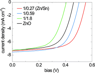 | ||
| Fig. 3 Current–voltage characteristics of the devices with different a-ZTO buffer layer cation ratios under 1 Sun illumination (AM1.5G spectrum). | ||
| Buffer layer | Zn/Sn | Averaged | Best cells | |||||||
|---|---|---|---|---|---|---|---|---|---|---|
| Number of cellsa | V OC (mV) | J SC (mA cm−2) | FF (%) | Efficiency (%) | V OC (mV) | J SC (mA cm−2) | FF (%) | Efficiency (%) | ||
| a Fully shunted devices were excluded. | ||||||||||
| ZnO | — | 18 | 444 ± 17 | 7.20 ± 0.11 | 59.4 ± 1.9 | 1.90 ± 0.12 | 462 | 7.26 | 61.8 | 2.07 |
| a-ZTO | 1/0.27 | 17 | 543 ± 05 | 7.34 ± 0.11 | 62.9 ± 2.9 | 2.51 ± 0.15 | 553 | 7.37 | 65.0 | 2.65 |
| a-ZTO | 1/0.59 | 17 | 496 ± 09 | 7.50 ± 0.12 | 61.5 ± 4.7 | 2.29 ± 0.22 | 503 | 7.56 | 63.4 | 2.41 |
| a-ZTO | 1/1.8 | 18 | 382 ± 26 | 7.28 ± 0.08 | 54.2 ± 5.1 | 1.52 ± 0.22 | 406 | 7.25 | 58.2 | 1.72 |
To determine the mechanism whereby the a-ZTO buffer layer increases the device performance, the band alignment relative to the Cu2O layer is characterized by photoelectron spectroscopy following the procedure outlined by Waldrop et al. (Fig. S2–S5†).27 An X-ray (Al-Kα) photon source is used to measure the binding energies of Cu and Zn core levels with respect to the valence band maximum energy of Cu2O and a-ZTO bulk film samples. Two-layer samples that consist of 2.5 µm thick Cu2O films covered by ∼2 nm thick a-ZTO films are used to measure valence-band energy alignments. The optical (Tauc) gap values are added to estimate conduction-band positions. Fig. 4a shows the estimated band alignments of a-ZTO overlayers on Cu2O films. The Cu2O–ZnO interface yields a conduction-band offset (ΔECB) of −1.47 ± 0.2 eV (cliff), comparable to previous reports.28,29 All a-ZTO layers are expected to create a conduction band “barrier” greater than 0.3 eV, which can prevent electrons in the AZO layer from recombining with holes in the Cu2O layer, while allowing photo-generated electrons in the Cu2O layer to be collected at the AZO layer.11
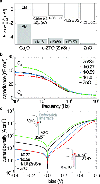 | ||
| Fig. 4 (a) Relative alignments of conduction-band (CB) and valence-band (VB) energies for a-ZTO and ZnO overlayers to Cu2O thin films investigated in this work, as measured by XPS and optical absorption. (b) Room-temperature capacitance–frequency characteristics of the devices with a-ZTO and ZnO buffer layers measured with 0 V (DC) and 0.01 V (AC) bias under dark conditions. (c) Effect of a-ZTO buffer layers on dark current density vs. voltage characteristics of the devices. Inset schematics at the top and bottom show electronic band structures of the devices with ZnO and a-ZTO (Zn/Sn = 1/0.27) buffer layers, respectively. Grey areas indicate defect-rich interfaces with deep trap states. Red arrow lines represent interface recombination paths for electrons (filled circles) from the AZO layer. The a-ZTO (Zn/Sn = 1/0.27) buffer layer impedes electron movement to the interface where holes (open circles) are provided from the Cu2O layer, which reduces J0 by nearly a factor of ∼40 compared to the control device (ZnO buffer layer). | ||
While the presence of a conduction-band barrier explains the improved performance of the Zn-rich buffer layer, it does not explain the performance reduction observed for increasing Sn concentrations in the buffer layer. We hypothesize that the reduced performance for the Sn-rich buffer layer is due to an increase of subgap states in the buffer layer. Room-temperature capacitance–frequency (C–f) measurements are performed (Fig. 4b); the frequency dependence of diode capacitance is used to measure the densities and energy levels of trap states present in the depletion region.30 At high frequencies, the device behaves like an insulator due to dielectric freeze-out and exhibits a geometric capacitance (Cg). The Cg can be calculated using the relationship Cg = εA/t, where ε is the dielectric constant, A is the device area, and t is the thickness of the Cu2O layer. At frequencies near 1 MHz, capacitances of all devices converge to 4.5–4.7 nF cm−2, close to Cg of the device (∼2.7 nF cm−2). At low frequencies, the capacitance of all devices plateaus to a depletion capacitance (Cd), which is affected by charging and discharging of interface and bulk defect levels present in the depletion region.31 The highest efficiency device exhibits the lowest Cd, indicative of lower defect densities. On the other hand, the device exhibiting the highest Cd has the lowest VOC and is Sn-rich (1/1.8). All devices have identical geometry and fabrication processes except for the 5 nm thick buffer layers. Also, all buffer layer depositions are initiated with a ZnO sub-cycle to maintain the same atomic interface with the Cu2O layer. Thus, the relative change in Cd is likely caused by defects originating from subgap states within the a-ZTO buffer layer. The increased density of subgap states likely promotes recombination, decreasing VOC. Preliminary evidence of increased subgap states in Sn-rich a-ZTO films is provided in Fig. S4.† Although these appear to be “bulk” defect states within the a-ZTO, henceforth we refer to these as “interface states,” given the nanometer-scale thickness of the buffer layer.
The VOC of a heterojunction solar cell is strongly affected by the density and energy levels of interface traps, which increase the dark saturation current by promoting interface recombination.32 The VOC can be estimated as:
 | (1) |
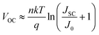
Additional improvements to VOC can be gained by enhancing JSC, as given in eqn (1). Due to the low carrier density of electrochemically deposited Cu2O thin films (p = 1013 to 1014 cm−3), a fully depleted Cu2O layer is expected in our devices.33 The photo-generated carrier collection-probability profile in the Cu2O layer is modelled to decay exponentially with a minority carrier drift length (Ldrift), due to the high density of lifetime-limiting defects.34 We simulate optical absorption in the device by using the finite difference time domain (FDTD) method. The device is modelled as a two-dimensional geometry of AZO (80 nm)/a-ZTO (5 nm)/Cu2O (2.5 µm)/Au (200 nm), with surface texture determined by atomic force microscopy, under incident light with transverse magnetic mode polarization. We used the optical properties of Cu2O from ref. 35, since the electrochemically deposited Cu2O thin films are too textured to accurately measure the optical path length. Due to the textured top surface morphology and the light-reflecting Au bottom electrode, the device can absorb near band-edge photons effectively. The calculated spatial absorption profile for light with a wavelength of 500 nm is shown in Fig. 5a. We simulate EQE curves by weighting the generated minority carriers with the spatial collection probability functions with varying Ldrift (Fig. S6†). Using this method, we generate the EQE curves with calculated JSC as a function of Ldrift and plot measured EQE of the best performing device (1/0.27), as shown in Fig. 5b. The drop-off of EQE for λ < 380 nm is mostly due to absorption by the AZO and a-ZTO layers. The Ldrift of the a-ZTO device is estimated to be 0.6 µm, by comparing the EQE curves from the FDTD simulation and the actual measurement. The control device shows a similar EQE to the a-ZTO device, re-affirming that the a-ZTO buffer layer affects interface properties only (Fig. S7†). The simulated EQE curves indicate that a JSC of over 11 mA cm−2 may be possible by increasing the carrier collection efficiency. Improving carrier collection with longer Ldrift and light trapping will be an important next step toward achieving devices with higher efficiencies. Further VOC increases may be achieved by substituting the TCO and buffer layer materials for those with more similar conduction-band energies to Cu2O.
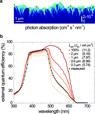 | ||
| Fig. 5 (a) Simulated optical absorption profile in the Cu2O layer for 500 nm wavelength light with the intensity in the AM1.5G spectrum. (b) Effect of the minority carrier drift length (Ldrift) of Cu2O on EQE and JSC. Coloured lines represent calculated EQE from optical simulation with a carrier collection probability profile with increasing Ldrift and an ideal 100% collection case. Numbers in parentheses indicate calculated JSC. The dotted black line represents measured EQE of the device with an a-ZTO (Zn/Sn = 1/0.27) buffer layer. | ||
In summary, we demonstrate an increase of power conversion efficiency of Cu2O-based all-metal-oxide thin film solar cells by introducing a 5 nm thick a-ZTO buffer layer between the absorber and TCO. The ALD fabrication process enables a conformal coverage to textured surfaces, as well as tunable electrical and optical properties of the a-ZTO films via the zinc-to-tin ratio. J–V measurements indicate that the efficiency increase results from the reduction in dark saturation current density. The band-alignment and C–f measurements indicate a reduction of interface recombination, resulting from an electron-blocking barrier by the a-ZTO layer with a low density of trap-states. Due to the highly conformal coverage and precise thickness control by ALD, only a 5 nm thick buffer layer is necessary to improve the junction quality without sacrificing carrier transport and optical transmission. This approach to improve device efficiencies may be extended to other Earth-abundant heterojunction photovoltaic cells.
Experimental
Atomic layer deposition of a-ZTO and AZO thin films
Amorphous-ZTO, AZO, and undoped ZnO thin films were synthesized by ALD using a custom-built hot-wall reactor at 120 °C. A cyclic amide of tin (1,3-bis(1,1-dimethylethyl)-4,5-dimethyl-(4R,5R)-1,3,2-diazastannolidin-2-ylidene)Sn(II) and diethyl zinc (Sigma Aldrich) were used as Sn and Zn precursors, respectively.16,19 A 50 wt% hydrogen peroxide (H2O2) solution was used as a common oxidant for a-ZTO growth. A constant flow of N2 carrier gas was employed during the ALD of ZTO.16 The tin precursor and diethyl zinc were held at 40 and 25 °C and their equilibrium vapour pressures were estimated to be 0.42 and 6.8 Torr, respectively. The exposures of the tin precursor and diethyl zinc were estimated to be around 0.33 and 0.032 Torr s in each cycle, respectively. The exposures of H2O2 and H2O were about 0.027 and 4.4 Torr s, respectively. To deposit a-ZTO films, an ALD super-cycle scheme with ZnO and SnO2 sub-cycles was employed. Three different ZnO/SnO2 sub-cycle ratios of 3/1, 1/1, 1/3 were used to find the optimized composition as a buffer layer in the Cu2O–ZnO heterojunction. Their nominal growths per one super-cycle were 3.1, 1.6 and 4.1 Å, respectively, measured by X-ray reflectivity. AZO thin films were also synthesized at 120 °C by ALD using diethyl zinc, trimethylaluminum and de-ionized water as Zn, Al precursors and oxidant, respectively. An optimized Al2O3 doping ratio to ZnO (1 cycle of Al2O3 after every 19 cycles of ZnO) was selected to obtain the lowest resistivity (5.9 × 10⁻³ Ω cm) of the films. The nominal film growth per one super-cycle, which consists of 19-ZnO and 1-Al2O3 sub-cycles, was 32 Å. Undoped ZnO as a control buffer layer was grown at 120 °C without Al doping with de-ionized water as an oxidant.Thin film solar cell fabrication
An Au bottom electrode (200 nm thick, 3.2 cm2 area) with a 5 nm thick Ti adhesion layer was deposited on a 1 × 1 inch2 fused silica by e-beam evaporation. A 2.5 µm thick Cu2O film was deposited on the Au film at 40 °C by the galvanostatic electrochemical method.36 A lactate-stabilized copper sulfate aqueous solution was prepared with 3 M lactic acid (Sigma Aldrich), 0.2 M cupric sulfate pentahydrate (CuO4S·5H2O, Sigma Aldrich) and de-ionized water (18.3 MΩ cm, Ricca Chemical) was prepared and 2 M sodium hydroxide (NaOH, Sigma Aldrich) aqueous solution was added to adjust the pH of the solution to 12.5. All reagent-grade chemicals were used and the solution was filtered and stirred thoroughly. A constant current density of 0.23 mA cm−2 was applied using a Keithley 2400 sourcemeter with a Pt counter electrode to grow the Cu2O films. The Cu2O film surfaces were rinsed with de-ionized water. Amorphous-ZTO and polycrystalline AZO layers were deposited by ALD, followed by Al electrode deposition. The Al electrodes (300 nm thick) were deposited by e-beam evaporation with a grid spacing of 1 mm defined by a shadow mask. A 3 × 5 mm2 cell area was defined by photolithography and wet etching with a nitric acid solution.Characterization
The microstructures of the films were characterized by JEM-2100 HR-TEM (JEOL) and GAXRD using a PANalytical X'Pert Pro diffractometer with Cu-Kα radiation (ω = 0.9°). Surface morphologies of the grown films were analysed using an Ultra 55 FESEM (Zeiss). Optical properties of the films were measured using a U-4100 UV-VIS spectrophotometer (Hitachi) and a VASE spectroscopic ellipsometer (J. A. Woollam Co., Inc.). Electrical properties of the films were characterized by Hall effect measurements using the van der Pauw configuration and a magnetic field of 0.75 T. XPS and UPS measurements were performed using a PHI VersaProbe II (Physical Electronics) and an AXIS Nova (Kratos analytical, KBSI Jeonju, Korea). Samples were etched by an Ar ion beam to remove carbon contaminants on the surface. The current–voltage and the capacitance–frequency characteristics of the device were measured by using Agilent 4156C and Keithley 4200 semiconductor characterization systems. The standard 1 Sun illumination was generated by a Newport Oriel 91194 solar simulator with a 1300 W Xe-lamp with a AM1.5G filter and a Newport Oriel 68951 flux controller calibrated by an NREL-certified Si reference cell equipped with a BG-39 window. No intentional light-soaking was applied to the devices. EQE of the device was measured using a QEX7 (PV Measurements, Inc.) calibrated by a NIST-certified Si photodiode. The top surface morphology of the device was measured by atomic force microscopy using a MFP-3D SA (Asylum Research).Acknowledgements
The authors thank Dr I. Kozinsky (Bosch), B. Son (KBSI), and K. Broderick (MIT) for helpful discussions and experimental support. F. Frankel (MIT) is thanked for helpful advice on graphics. This work was supported by the Chesonis Family Foundation, Bosch through the MIT Energy Initiative, NSF award CBET-1032955, and NSF CAREER award ECCS-1150878. This work made use of the MTL and CMSE at MIT and the CNS at Harvard University supported by NSF awards DMR-0819762 (CMSE) and ECS-0335765 (CNS). A Clean Energy Scholarship from NRF Singapore (S.C.S.) and an NSF Graduate Research Fellowship (R.E.B.) are acknowledged.Notes and references
- C. Wadia, A. P. Alivisatos and D. M. Kammen, Environ. Sci. Technol., 2009, 43, 2072–2077 CrossRef CAS.
- K. P. Musselman, A. Wisnet, D. C. Iza, H. C. Hesse, C. Scheu, J. L. MacManus-Driscoll and L. Schmidt-Mende, Adv. Mater., 2010, 22, E254–E258 CrossRef CAS.
- S. Rühle, A. Y. Anderson, H.-N. Barad, B. Kupfer, Y. Bouhadana, E. Rosh-Hodesh and A. Zaban, J. Phys. Chem. Lett., 2012, 3, 3755–3764 CrossRef.
- B. K. Meyer, A. Polity, D. Reppin, M. Becker, P. Hering, P. J. Klar, T. Sander, C. Reindl, J. Benz, M. Eickhoff, C. Heiliger, M. Heinemann, J. Bläsing, A. Krost, S. Shokovets, C. Müller and C. Ronning, Phys. Status Solidi B, 2012, 249, 1487–1509 CrossRef CAS.
- C. Xiang, G. M. Kimball, R. L. Grimm, B. S. Brunschwig, H. A. Atwater and N. S. Lewis, Energy Environ. Sci., 2011, 4, 1311–1318 CAS.
- Y. Nishi, T. Miyata and T. Minami, Thin Solid Films, 2013, 528, 72–76 CrossRef CAS.
- M. Izaki, T. Shinagawa, K. T. Mizuno, Y. Ida, M. Inaba and A. Tasaka, J. Phys. D: Appl. Phys., 2007, 40, 3326–3329 CrossRef CAS.
- S. Jeong, S. H. Song, K. Nagaich, S. A. Campbell and E. S. Aydil, Thin Solid Films, 2011, 519, 6613–6619 CrossRef CAS.
- K. P. Musselman, A. Marin, A. Wisnet, C. Scheu, J. L. MacManus-Driscoll and L. Schmidt-Mende, Adv. Funct. Mater., 2011, 21, 573–582 CrossRef CAS.
- M. Taguchi, A. Terakawa, E. Maruyama and M. Tanaka, Prog. Photovoltaics, 2005, 13, 481–488 CAS.
- T. Minemoto, T. Matsui, H. Takakura, Y. Hamakawa, T. Negami, Y. Hashimoto, T. Uenoyama and M. Kitagawa, Sol. Energy Mater. Sol. Cells, 2001, 67, 83–88 CrossRef CAS.
- J. Robertson, Phys. Status Solidi B, 2008, 245, 1026–1032 CrossRef CAS.
- A. Walsh, J. L. F. D. Silva and S.-H. Wei, J. Phys.: Condens. Matter, 2011, 23, 334210 CrossRef.
- E. Fortunato, P. Barquinha and R. Martins, Adv. Mater., 2012, 24, 2945–2986 CrossRef CAS.
- K. Nomura, H. Ohta, A. Takagi, T. Kamiya, M. Hirano and H. Hosono, Nature, 2004, 432, 488–492 CrossRef CAS.
- J. Heo, S. B. Kim and R. G. Gordon, Appl. Phys. Lett., 2012, 101, 113507 CrossRef.
- J. Lindahl, J. T. Wätjen, A. Hultqvist, T. Ericson, M. Edoff and T. Törndahl, Prog. Photovoltaics, 2012 DOI:10.1002/pip.2239.
- Z. Zhang, W. Hu, Y. Deng, C. Zhong, H. Wang, Y. Wu and L. Liu, Mater. Res. Bull., 2012, 47, 2561–2565 CrossRef CAS.
- J. Heo, A. S. Hock and R. G. Gordon, Chem. Mater., 2010, 22, 4964–4973 CrossRef CAS.
- H. Q. Chiang, J. F. Wager, R. L. Hoffman, J. Jeong and D. A. Keszler, Appl. Phys. Lett., 2005, 86, 013503 CrossRef.
- J.-Y. Kwon, D.-J. Lee and K.-B. Kim, Electron. Mater. Lett., 2011, 7, 1–11 CrossRef CAS.
- T. Moriga, Y. Hayashi, K. Kondo, Y. Nishimura, K.-i. Murai, I. Nakabayashi, H. Fukumoto and K. Tominaga, J. Vac. Sci. Technol., A, 2004, 22, 1705–1710 CAS.
- Y.-H. Kim, J.-S. Heo, T.-H. Kim, S. Park, M.-H. Yoon, J. Kim, M. S. Oh, G.-R. Yi, Y.-Y. Noh and S. K. Park, Nature, 2012, 489, 128–132 CrossRef CAS.
- S. Narushima, H. Mizoguchi, K. Shimizu, K. Ueda, H. Ohta, M. Hirano, T. Kamiya and H. Hosono, Adv. Mater., 2003, 15, 1409–1413 CrossRef CAS.
- K. Satoh, Y. Kakehi, A. Okamoto, S. Murakami, F. Uratani and T. Yotsuya, Jpn. J. Appl. Phys., 2005, 44, L34–L37 CrossRef CAS.
- J. S. Rajachidambaram, S. Sanghavi, P. Nachimuthu, V. Shutthanandan, T. Varga, B. Flynn, S. Thevuthasan and G. S. Herman, J. Mater. Res., 2012, 27, 2309–2317 CrossRef CAS.
- J. R. Waldrop, R. W. Grant, S. P. Kowalczyk and E. A. Kraut, J. Vac. Sci. Technol., A, 1985, 3, 835–841 CAS.
- Z. Q. Duan, A. Du Pasquier, Y. C. Lu, Y. Xu and E. Garfunkel, Sol. Energy Mater. Sol. Cells, 2012, 96, 292–297 CrossRef CAS.
- L. M. Wong, S. Y. Chiam, J. Q. Huang, S. J. Wang, J. S. Pan and W. K. Chim, J. Appl. Phys., 2010, 108, 033702 CrossRef.
- T. Walter, R. Herberholz, C. Muller and H. W. Schock, J. Appl. Phys., 1996, 80, 4411–4420 CrossRef CAS.
- T. Eisenbarth, T. Unold, R. Caballero, C. A. Kaufmann and H.-W. Schock, J. Appl. Phys., 2010, 107, 034509–034512 CrossRef.
- M. Saad and A. Kassis, Sol. Energy Mater. Sol. Cells, 2003, 79, 507–517 CrossRef CAS.
- K. P. Musselman, A. Marin, L. Schmidt-Mende and J. L. MacManus-Driscoll, Adv. Funct. Mater., 2012, 22, 2202–2208 CrossRef CAS.
- K. P. Musselman, Y. Ievskaya and J. L. MacManus-Driscoll, Appl. Phys. Lett., 2012, 101, 253503 CrossRef.
- C. Malerba, F. Biccari, C. L. A. Ricardo, M. D'Incau, P. Scardi and A. Mittiga, Sol. Energy Mater. Sol. Cells, 2011, 95, 2848–2854 CrossRef CAS.
- P. E. de Jongh, D. Vanmaekelbergh and J. J. Kelly, Chem. Mater., 1999, 11, 3512–3517 CrossRef CAS.
Footnotes |
| † Electronic supplementary information (ESI) available. See DOI: 10.1039/c3ee24461j |
| ‡ Both authors contributed equally to this work. |
| This journal is © The Royal Society of Chemistry 2013 |