 Open Access Article
 This Open Access Article is licensed under a Creative Commons Attribution-Non Commercial 3.0 Unported Licence
Enhancement of PbS quantum dot-sensitized photocurrents using plasmonic gold nanoparticles†
Tokuhisa
Kawawaki
and
Tetsu
Tatsuma
*
Institute of Industrial Science, The University of Tokyo, 4-6-1 Komaba, Meguro-ku, Tokyo 153-8505, Japan. E-mail: tatsuma@iis.u-tokyo.ac.jp; Fax: +81-3-5452-6338; Tel: +81-3-5452-6336
First published on 15th October 2013
Abstract
For improvement of the conversion efficiency of solar cells, it is important to make effective use of near-infrared light, which accounts for about 40% of sunlight energy. Although solar cells based on quantum dots (QDs) such as PbS have been studied for the use of near-infrared light, their photoabsorption is not necessarily sufficient. In this study, we coupled PbS QD-sensitized solar cells with plasmonic Au nanoparticles (NPs) as light-harvesting antennae. As a result, the photocurrents of the cells were enhanced in the visible and near-infrared regions (500–1200 nm) due to interparticle plasmon coupling of spherical Au NPs. The maximum enhancement factor was 6. We also found that the optimum QD–NP spacing is shorter and that the maximum enhancement factor is higher when smaller QDs are used. These results suggest that a negative effect, quenching via energy transfer from QD to NP, is less significant for smaller PbS QDs.
1 Introduction
Quantum dot solar cells (QDSCs) prepared using a chemical process attract attention as one of the cost-effective and efficient next generation solar cells.1 QDs are semiconductor nanoparticles with diameters smaller than the Bohr radius of their exciton. QDSCs are characterized by high quantum efficiency and optical and thermal stability.2 It is easy to control the light absorption wavelength of QDs by changing their size. Therefore, absorption spectrum of a QDSC can be matched to the solar spectrum.3 An additional advantage of QDSCs is the multiple exciton generation (MEG), which improves energy usage due to generation of two or more electron–hole pairs by a single photon with energy at least twice the bandgap energy.2,4,5 Chemically processed QDSCs are generally categorized into (1) Schottky junction QDSCs,6 (2) hetero-junction QDSCs,7,8 and (3) QD-sensitized solar cells (QDSSCs).9–11 Although chemically processed QDSCs have achieved high external quantum efficiency (EQE) in the visible light region (80% at 400 nm), the efficiency is relatively low in the near-infrared region (30% at 1000 nm).8 In order to improve the EQE, it is necessary to increase the light absorption in the near-infrared region. However, if the QD layer is thickened for an increased absorption, the internal resistance of the cell also increases.Recently, it has been reported that plasmonic metal nanoparticles (NPs) such as Au12–14 and Ag15–17 NPs enhance photocurrents of solar cells. The enhancement effect is believed to be based on localized surface plasmon resonance (LSPR) of the NPs. The NP collects photons by LSPR, and generates a strong oscillating electric field (i.e. optical near field) that is localized in the vicinity of the NP.18 The localized electric field can enhance the photocurrents by exciting electrons of dye molecules or semiconductor more efficiently than incident far field light. In the previous studies of the absorption enhancement of QDSCs by plasmonic NPs, the absorption edge wavelengths of the QDs and NPs employed were 900 nm and 800 nm, respectively, or shorter.19,20 We have recently shown that Ru dye-sensitized photocurrents can be enhanced even in the near-infrared region by using an interparticle plasmon coupling effect of spherical NPs, without using anisotropic NPs such as nanorods, which are thermally less stable.21 However, since the absorption edge wavelength of the dye used was shorter than 900 nm, photocurrent enhancement in the longer wavelength region has not been achieved. Based on these, here we used PbS QDs, the absorption edge of which is 1300 nm, to verify the plasmonic enhancement effect in the near-infrared region. We also examined the influence of the QD–NP spacing and the QD size on the enhancement effect. Thus obtained results would contribute to effective use of near-infrared light for solar cells, photocatalysts and improvement in efficiency of fluorescence and electroluminescence of QDs.
In this work we prepare two-dimensional indium tin oxide (ITO)/Au NP/TiO2/QD photoelectrodes (Fig. 1a), in which the QD–NP spacing can be controlled by changing the TiO2 thickness.13,16,19,21 The present system also allows us to examine effects of the QD size. If we deposit QDs in a nanoporous TiO2 film, which is used for conventional dye-sensitized solar cells, QD suppresses transport of redox species in the nanopores, as the QD size increases. Therefore, dependence of the enhancement on the QD size cannot be separated from the mass transport effect. Our objective is a fair comparison of the photoelectrodes containing Au NPs (Fig. 1a) with those without Au NPs (Fig. 1b).
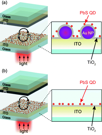 | ||
| Fig. 1 Schematic illustration of (a) the photoelectrochemical cell with the ITO/Au NP/TiO2/PbS QD electrode and (b) that with the ITO/TiO2/PbS QD electrode. | ||
2 Experimental section
2.1 Preparation of the photoelectrodes
Smooth ITO-coated glass plates (Kuramoto) were modified using (3-aminopropyl)triethoxysilane, and Au NPs (diameter = 100 nm, Tanaka Kikinzoku) were immobilized onto the surface. The ITO with or without Au NPs was coated with a thin TiO2 film prepared using a spray pyrolysis method.13,21,22 The thickness of the TiO2 films was determined based on scanning electron microscopy (SEM) data to be 5–35 nm (ESI†). The thickness was 9.0 ± 2.5 nm (mean ± standard deviation, n = 8) unless otherwise noted. It was also confirmed using SEM that Au NPs were completely and evenly coated with the TiO2 films.13 PbS QDs23 were prepared using the successive ionic layer adsorption and reaction (SILAR) method9–11 through alternate spin-coating with water–methanol solution (5![[thin space (1/6-em)]](https://www.rsc.org/images/entities/char_2009.gif) :95 by volume) of 5 mM Pb(NO3)2 and 5 mM Na2S. We characterized the deposited PbS QDs using SEM and atomic force microscopy (AFM). X-ray diffraction patterns for the PbS QDs (20 SILAR cycles) showed that the particles are face-centered cubic PbS.24
:95 by volume) of 5 mM Pb(NO3)2 and 5 mM Na2S. We characterized the deposited PbS QDs using SEM and atomic force microscopy (AFM). X-ray diffraction patterns for the PbS QDs (20 SILAR cycles) showed that the particles are face-centered cubic PbS.24
2.2 Photoelectrochemical measurements
Photocurrents of the obtained ITO/Au NP/TiO2/QD or ITO/TiO2/QD electrode (electrode area = 0.196 cm2) were examined by constructing a two-electrode cell (Fig. 1) with a platinum-coated ITO counter electrode. The gap between the electrodes (50 μm) was filled with N2-saturated water containing 0.1 M Na2S.25 Short-circuit photocurrents were measured using a potentiostat (SI1280B, Solartron) under light at 460–1400 nm at a constant photon flux (6.0 × 10¹⁵ photons cm−2 s−1) from a xenon lamp (460–900 nm) or a halogen lamp (1000–1400 nm) equipped with a band-pass filter (full width at half-maximum = 10 nm). The drift of the photocurrent during a series of measurements was smaller than 11%.3 Results and discussion
3.1 Absorption and amounts of deposited PbS QDs
First we prepared ITO/TiO2/QD electrodes (Fig. 1b). The PbS QDs were deposited on the TiO2 thin film (9 nm thick) using the SILAR method.9–11 It is known that the average QD size increases as the SILAR cycle is repeated.26 Actually, the height of the PbS QDs prepared by 2, 5 and 10 SILAR cycles was evaluated using AFM (Fig. 2a–c) to be 5.2 ± 0.2 nm, 9.1 ± 0.5 nm and 15.2 ± 0.7 nm, respectively (mean ± standard deviation, n = 15).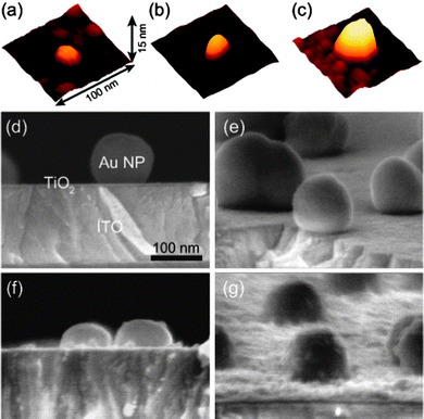 | ||
| Fig. 2 (a–c) AFM images of PbS QDs (2, 5 and 10 SILAR cycles for a, b and c, respectively) on the TiO2 surface and SEM images of (d) ITO/Au NP/TiO2 and (e–g) ITO/Au NP/TiO2/PbS QD (2, 5 and 10 SILAR cycles for b, c and d, respectively) electrodes. ANP/AE = 0.05 and TiO2 thickness = 9 nm. | ||
The QDs exhibit light absorption in the visible and near-infrared region (Fig. 3a). As the number of SILAR cycles increased from 2 to 10, the absorption edge wavelength was redshifted from 800 to 1300 nm. This redshift indicates a decrease in the bandgap of the QDs. The redshift is reasonable because it is known that the bandgap decreases as the QD size increases.
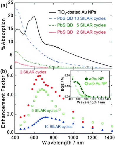 | ||
| Fig. 3 (a) Absorption spectra of TiO2-coated Au NPs on ITO and PbS QDs (2, 5 and 10 SILAR cycles) on TiO2 and (b) action spectra of photocurrent enhancement factor for ITO/Au NP/TiO2/PbS QD electrodes. Inset shows action spectra of EQE of the electrode with and without Au NPs (5 SILAR cycles). ANP/AE = 0.05 and TiO2 thickness = 9 nm. | ||
Next we embedded 100 nm diameter Au NPs into the TiO2 thin film (9 nm thick) to obtain ITO/Au NP/TiO2/QD electrodes (Fig. 1a). The occupancy of the NPs, ANP/AE, where ANP is the projected area of Au NPs and AE is that of the electrode surface, was 0.05. We have reported previously that the interparticle spacing of some Au NPs is short enough at ANP/AE = 0.05 to exhibit the plasmon coupling effect so that NPs absorb near-infrared light and generate localized electric field even at >850 nm.21 Actually, the sample thus obtained exhibits an absorption even in the near-infrared region. The peak and the absorption edge were observed at ∼600 nm and >1400 nm, respectively (Fig. 3a). The absorption band overlaps well with that of the PbS QDs, so that it is expected that the Au NPs enhance the absorption of the QDs.
Fig. 2e–g shows SEM images of the electrodes prepared by 2, 5 and 10 SILAR cycles. Amounts of PbS QDs deposited on the ITO/Au NP/TiO2 electrode (WAu) were measured and compared with those deposited on the ITO/TiO2 electrode (Wcontrol). PbS QDs on an electrode were dissolved in 1 M HNO3 (3 mL) and the amount of Pb2+ in the solution was determined using inductively coupled plasma-mass spectrometry (ICP-MS). Ratios of the PbS amount WAu/Wcontrol were determined to be 1.11 ± 0.08, 1.20 ± 0.09 and 1.23 ± 0.19 (mean ± standard deviation, n = 3), for QDs prepared by 2, 5 and 10 SILAR cycles, respectively.
3.2 Enhancement of QD-sensitized photocurrents
Next we examined effects of the Au NPs on QD-sensitized photocurrents. We prepared thin layer cells (Fig. 1) and observed anodic short-circuit photocurrents for the ITO/Au NP/TiO2/QD and ITO/TiO2/QD electrodes prepared by 5 SILAR cycles. External quantum efficiencies (EQE) for QD electrodes with and without Au NPs are plotted against the irradiation wavelength in the inset of Fig. 3b. The anodic photocurrents are ascribed to electron excitation from the valence band (VB) to the conduction band (CB) of PbS QDs and injection of the excited electrons to the TiO2 CB accompanied by electron transfer from the electron donor in the electrolyte (S2−) to the PbS VB4,23,25,27 (Fig. 4).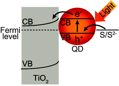 | ||
| Fig. 4 Schematic illustration of the photoinduced charge separation of the TiO2/QD system. | ||
Although there is concern that using large PbS QDs is disadvantageous for electron injection from the PbS CB to the TiO2 CB due to close energy levels,27 it is reported that the electron transfer is possible for PbS QDs of 9.9 nm diameter in a S/S2− electrolyte at pH 13.28 According to a previous report,29 it is expected that the CB level of PbS QDs shifts positively by about 60 mV as the QD size increases from 9.9 nm to 15 nm.29 On the other hand, in the S/S2− electrolyte at pH 12 used in this study, the TiO2 CB level is more positive by about 60 mV than that in ref. 28, because the TiO2 CB level shifts by −60 mV per pH.30 Therefore, it is reasonable that electrons transfer from PbS CB to TiO2 CB in our system.
It is clear from Fig. 3b (inset) that the electrode with Au NPs exhibits significantly higher photocurrents than the electrode without Au NPs. On the other hand, photocurrents from an ITO/Au NP/TiO2 electrode without PbS QD was negligibly small (<10 nA). Although it is known that plasmon-induced charge separation is often observed at the Au NP/TiO2 interface,31–33 the TiO2 film used in this work (9 nm) is too thin to observe the plasmon-induced charge separation.33 Therefore, the photocurrent increased by the introduction of Au NPs is attributed to enhancement of the QD-sensitized photocurrents.
To reveal the dependence of the enhancement on the irradiation wavelength, we evaluated the photocurrent enhancement factor from the photocurrents for ITO/Au NP/TiO2/QD electrodes (IAu), those for ITO/TiO2/QD electrodes (Icontrol) and the ratio of the QD amount (WAu/Wcontrol) as follows.
| Enhancement factor = (IAu/Icontrol)/(WAu/Wcontrol) | (1) |
The action spectrum of the enhancement factor for the electrode prepared by 5 SILAR cycles is shown in Fig. 3b (square). The photocurrent enhancement was significant in the wavelength range of 500–1200 nm, at which the Au NPs exhibit plasmon resonance as Fig. 3a shows (absorption of Au NPs at <500 nm is ascribed to interband transitions). These results indicate that the photocurrents are enhanced by LSPR of the Au NPs. The maximum enhancement factor is 4.6.
3.3 Effects of the QD size
The photocurrent enhancement was also examined for smaller and larger QDs (2 and 10 SILAR cycles, respectively) as shown in Fig. 3b. The TiO2 thickness was 9 nm. It is obvious from the figure that the maximum enhancement factor decreases as the SILAR cycle increases. In the present system, it is likely that photoabsorption of QDs is enhanced as a result of excitation by the localized electric field (i.e. optical near field) in the vicinity of the plasmonic Au NPs.12–17 Such an enhancement effect strongly depends on the distance from the NP.13,16,19,21,34,35 We therefore examined dependence of the enhancement factor on the TiO2 thickness (i.e. the QD–NP spacing) (Fig. 5).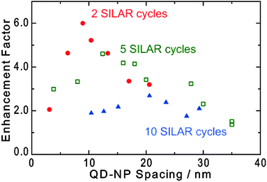 | ||
| Fig. 5 Maximum photocurrent enhancement factor of ITO/Au NP/TiO2/PbS QD electrodes as a function of the QD–NP spacing. ANP/AE = 0.05. | ||
As the PbS QD approaches Au NP, the enhancement factor increases gradually, then decreases when the spacing is too short. A similar behavior has been observed for other photocurrent enhancement systems.13,19,21,34,35 The initial increase in the enhancement factor is explained in terms of the intensifying electric field from the Au NP as the QD approaches the NP. The final drop of the enhancement is attributed to Förster resonance energy transfer (FRET)36–39 from excited QDs to NPs occurring before electron injection from the excited QDs into the TiO2 CB. Namely, the balance between the positive enhancement effect due to the plasmonic near field and the negative quenching effects due to FRET determines the optimum spacing and the highest enhancement.
Here we found that the optimum QD–NP spacing increases from ∼10 nm to ∼20 nm and that the maximum enhancement factor decreases from 6.0 to 2.7, as the QD size increases from ∼5 nm to ∼15 nm (i.e. the SILAR cycle is increased from 2 to 10). Since FRET is caused by the dipole–dipole interaction between QD and NP and the interaction intensifies with increasing dipole moment, it is reasonable to consider that larger QDs transfer energy to Au NPs more efficiently. Actually, it has been reported that fluorescence of larger CdTe QDs is more severely quenched by Au NPs.39 This also suggests that the energy transfer is accelerated as the QD size increases. Although back electron transfer might also cause a photocurrent decrease, it cannot explain the dependence of the photocurrent enhancement on the QD size.
These results indicate that larger QDs transfer energy over a longer distance (i.e. the Förster distance is longer) and thereby suppress the enhancement more significantly. Incidentally, the slight redshift of the enhancement peak with increasing QD size observed in Fig. 3b can be explained in terms of the redshift of the absorption wavelength (Fig. 3a) as well as the quenching wavelength. So far, it has been reported that the optimum QD–NP distance increases with increasing NP size.34 We therefore conclude that we can expect greater enhancement with smaller QDs and smaller NPs.
4 Conclusions
In conclusion, anodic photocurrents from TiO2 electrodes modified with PbS QDs were enhanced using plasmonic Au NPs in the visible and near-infrared regions (500–1200 nm). The maximum enhancement factor was 6. The enhancement was higher for smaller QDs because of suppressed quenching.Acknowledgements
This work was conducted as a part of “R&D on Innovative PV Power Generation Technology” which The University of Tokyo contracted with New Energy and Industrial Technology Development Organization (NEDO).Notes and references
- M. Graetzel, R. A. L. Janssen, D. B. Mitzi and E. H. Sargent, Nature, 2012, 488, 304–312 CrossRef CAS PubMed.
- J. Tang and E. H. Sargent, Adv. Mater., 2011, 23, 12–29 CrossRef CAS PubMed.
- X. H. Wang, G. I. Koleilat, J. Tang, H. Liu, I. J. Kramer, R. Debnath, L. Brzozowski, D. A. R. Barkhouse, L. Levina, S. Hoogland and E. H. Sargent, Nat. Photonics, 2011, 5, 480–484 CrossRef CAS.
- S. V. Kershaw, A. S. Susha and A. L. Rogach, Chem. Soc. Rev., 2013, 42, 3033–3087 RSC.
- O. E. Semonin, J. M. Luther, S. Choi, H. Y. Chen, J. B. Gao, A. J. Nozik and M. C. Beard, Science, 2011, 334, 1530–1533 CrossRef CAS PubMed.
- S. A. McDonald, G. Konstantatos, S. Zhang, P. W. Cyr, E. J. D. Klem, L. Levina and E. H. Sargent, Nat. Mater., 2005, 4, 138–142 CrossRef CAS PubMed.
- K. S. Leschkies, T. J. Beatty, M. S. Kang, D. J. Norris and E. S. Aydil, ACS Nano, 2009, 3, 3638–3648 CrossRef CAS PubMed.
- A. H. Ip, S. M. Thon, S. Hoogland, O. Voznyy, D. Zhitomirsky, R. Debnath, L. Levina, L. R. Rollny, G. H. Carey and A. Fischer, Nat. Nanotechnol., 2012, 7, 577–582 CrossRef CAS PubMed.
- D. J. Norris, K. S. Leschkies, R. Divakar, J. Basu, E. Enache-Pommer, J. E. Boercker, C. B. Carter, U. R. Kortshagen and E. S. Aydil, Nano Lett., 2007, 7, 1793–1798 CrossRef PubMed.
- H. Lee, M. K. Wang, P. Chen, D. R. Gamelin, S. M. Zakeeruddin, M. Grätzel and M. K. Nazeeruddin, Nano Lett., 2009, 9, 4221–4227 CrossRef CAS PubMed.
- P. K. Santra and P. V. Kamat, J. Am. Chem. Soc., 2012, 134, 2508–2511 CrossRef CAS PubMed.
- M. D. Brown, T. Suteewong, R. S. S. Kumar, V. D'Innocenzo, A. Petrozza, M. M. Lee, U. Wiesner and H. J. Snaith, Nano Lett., 2010, 11, 438–445 CrossRef PubMed.
- T. Kawawaki, Y. Takahashi and T. Tatsuma, Nanoscale, 2011, 3, 2865–2867 RSC.
- Y. Takahashi, S. Taura, T. Akiyama and S. Yamada, Langmuir, 2012, 28, 9155–9160 CrossRef CAS PubMed.
- C. Wen, K. Ishikawa, M. Kishima and K. Yamada, Sol. Energy Mater. Sol. Cells, 2000, 61, 339–351 CrossRef CAS.
- S. D. Standridge, G. C. Schatz and J. T. Hupp, J. Am. Chem. Soc., 2009, 131, 8407–8409 CrossRef CAS PubMed.
- M. Ihara, M. Kanno and S. Inoue, Physica E, 2010, 42, 2867–2871 CrossRef CAS.
- J. A. Schuller, E. S. Barnard, W. Cai, Y. C. Jun, J. S. White and M. L. Brongersma, Nat. Mater., 2010, 9, 193–204 CrossRef CAS PubMed.
- T. Kameyama, Y. Ohno, K. Okazaki, T. Uematsu, S. Kuwabata and T. Torimoto, J. Photochem. Photobiol., A, 2011, 221, 244–249 CrossRef CAS.
- J. Wu, S. C. Mangham, V. R. Reddy, M. O. Manasreh and B. D. Weaver, Sol. Energy Mater. Sol. Cells, 2012, 102, 44–49 CrossRef CAS.
- T. Kawawaki, Y. Takahashi and T. Tatsuma, J. Phys. Chem. C, 2013, 117, 5901–5907 CAS.
- Y. Tachibana, K. Umekita, Y. Otsuka and S. Kuwabata, J. Phys. D: Appl. Phys., 2008, 41, 102002 CrossRef.
- S. H. Im, H. Kim and S. Seok, Nanotechnology, 2011, 22, 395502 CrossRef PubMed.
- X. Wang, J. Zhuang, Q. Peng and Y. A. Li, Nature, 2005, 437, 121–124 CrossRef CAS PubMed.
- J. S. Hong, D. S. Choi, M. G. Kang, D. Kim and K.-J. Kim, J. Photochem. Photobiol., A, 2001, 143, 87–92 CrossRef CAS.
- R. Ahmed, G. Will, J. Bell and H. Wang, J. Nanopart. Res., 2012, 14, 1140 CrossRef.
- B. R. Hyun, Y. W. Zhong, A. C. Bartnik, L. F. Sun, H. D. Abruna, F. W. Wise, J. D. Goodreau, J. R. Matthews, T. M. Leslie and N. F. Borrelli, ACS Nano, 2008, 2, 2206–2212 CrossRef CAS PubMed.
- J. B. Sambur, T. Novet and B. A. Parkinson, Science, 2010, 330, 63–66 CrossRef CAS PubMed.
- J. Jasieniak, M. Califano and S. E. Watkins, ACS Nano, 2011, 5, 5888–5902 CrossRef CAS PubMed.
- A. Fujishima, A. Sakamoto and K. Honda, Seisan Kenkyu, 1969, 21, 450–452 CAS.
- Y. Tian and T. Tatsuma, J. Am. Chem. Soc., 2005, 127, 7632–7637 CrossRef CAS PubMed.
- T. Tatsuma, Bull. Chem. Soc. Jpn., 2013, 86, 1–9 CrossRef CAS.
- N. Sakai, Y. Fujiwara, Y. Takahashi and T. Tatsuma, ChemPhysChem, 2009, 10, 766–769 CrossRef CAS PubMed.
- T. Torimoto, H. Horibe, T. Kameyama, K. Okazaki, S. Ikeda, M. Matsumura, A. Ishikawa and H. Ishihara, J. Phys. Chem. Lett., 2011, 2, 2057–2062 CrossRef CAS.
- A. Kogo, Y. Takahashi, N. Sakai and T. Tatsuma, Nanoscale, 2013, 5, 7855–7860 RSC.
- O. Kulakovich, N. Strekal, A. Yaroshevich, S. Maskevich, S. Gaponenko, I. Nabiev, U. Woggon and M. Artemyev, Nano Lett., 2002, 2, 1449–1452 CrossRef CAS.
- I. L. Medintz, H. T. Uyeda, E. R. Goldman and H. Mattoussi, Nat. Mater., 2005, 4, 435–446 CrossRef CAS PubMed.
- Z. Nie, A. Petukhova and E. Kumacheva, Nat. Nanotechnol., 2010, 5, 15–25 CrossRef CAS PubMed.
- X. Zhang, C. A. Marocico, M. Lunz, V. A. Gerard, Y. K. Gun'ko, V. Lesnyak, N. Gaponik, A. S. Susha, A. L. Rogach and A. L. Bradley, ACS Nano, 2012, 6, 9283–9290 CrossRef CAS PubMed.
Footnote |
| † Electronic supplementary information (ESI) available. See DOI: 10.1039/c3cp53625d |
| This journal is © the Owner Societies 2013 |