 Open Access Article
 This Open Access Article is licensed under a
 Creative Commons Attribution 3.0 Unported Licence
Study of underpotential deposited Cu layers on Pt(111) and their stability against CO and CO2 in perchloric acid
Christian Schlaup* and Sebastian Horch
Department of Physics, Technical University of Denmark, DK–2800 Kongens Lyngby, Denmark. E-mail: cgsc@fysik.dtu.dk
First published on 4th October 2013
Abstract
The underpotential deposition (UPD) of copper on a Pt(111) electrode and the influence of gas coadsorbates, i.e. CO and CO2, on the thus deposited copper layer were studied in a 0.1 M HClO4 electrolyte by means of EC-STM. By UPD, an atomically flat Cu layer is formed, which exhibits a pseudomorphic (1 × 1) structure. However, it contains several point defects due to which its total coverage is less than a monolayer, in agreement with the measured charge density in the CV curves. Upon exposure to a CO-saturated solution the pseudomorphic structure collapses to a coalescent structure with many vacancy islands. This phase transition is induced by the preferential binding of CO to the Pt(111) surface. In contrast, CO2, which binds stronger to copper, does not affect the pseudomorphic structure of the Cu layer.
1 Introduction
The electrochemical phenomenon that certain amounts of a metal can be deposited above the Nernst potential is known as underpotential deposition (UPD).1 In contrast to bulk deposition at potentials below the Nernst potential, which is a continuous process, the UPD allows the deposition of metal adlayers with discrete and well defined coverages, generally covering the range of submonolayers to monolayers1,2 and for a few cases also multilayers, e.g. for silver on platinum.3,4The exact nature of these metal adlayers is not only determined by the involved metal species but also by the supporting electrolyte. Anions can coadsorb during the metal UPD and change the metal adlayer's structure and coverage. For example, even such a small concentration as 10−6 mol−1 of Cl− prevents the formation of a (2 × 2) phase during copper UPD on Au(111) electrodes.5 Also organic coadsorbates such as bis-(sodium-sulfopropyl)-disulfide (SPS) are known to influence the metal ad-/desorption and are used in industrial applications, such as the Damascene process.6 Coadsorbates can, however, not only affect the metal adlayer during the actual UPD, but also after deposition. This can be utilized, e.g., to form ultrathin binary compound films by consecutive steps of metal UPD and exposure to reactive anions, known as EC-ALE.7,8
In the present study, the response of an underpotential deposited copper adlayer on a Pt(111) surface to the adsorption of two complementary gasses, namely CO and CO2, was studied by means of EC-STM. CO and CO2 are complementary regarding their binding preferences: whereas CO binds strongly to platinum surfaces9 and even suppresses Cu UPD when present during deposition,10,11 CO2 binds stronger to copper.12 Using these two gasses thus allows for investigating the response of the copper adlayer in the two opposite cases of preferential gas–substrate interactions and preferential gas–metal adlayer interactions. This might also be relevant for electrochemical CO2 reduction, for which copper is the most active material and CO a key intermediate.13–17
2 Experimental
STM and CV measurements were carried out in a custom-built EC-STM setup,18 using electrochemically etched Pt/Ir (90/10) tunneling tips with a hot-glue (PEVAC) coating. The tip potential is set and held constant during potentiodynamic imaging with respect to the working electrode, corresponding to a constant bias voltage but variable tip potential. For all measurements, a Pt wire serves as a pseudo-reference electrode, which has a fair stability in acidic electrolytes, having a potential accuracy of ±25 mV. However, due to the high affinity of platinum for CO, a significant potential shift upon introduction of CO into the system is observed. The consequences of this potential shift will be discussed in the corresponding section in detail. In order to provide comparability, all potentials are given with respect to the standard hydrogen electrode (SHE), unless otherwise noted.A commercially available Pt(111) single crystal (MaTecK, Jülich) was prepared by flame annealing in a butane–air flame. After cooling down to room temperature in a high purity argon atmosphere (scientific grade, 99.9999%), it was protected with a droplet of ultrapure water and mounted into the electrochemical cell of the EC-STM.
Electrolyte solutions were prepared using ultrapure water (Millipore, Milli-Q®), 70% HClO4 (Merck, Suprapur®) and 99.9995% CuO (Alfa Aesar®). Before usage they were deaerated with argon (scientific grade, 99.9999%) and, if required, afterwards saturated with either CO (scientific grade, 99.997%) or CO2 (scientific grade, 99.9992%).
In order to avoid tip induced artifacts, a freshly prepared STM tip was used for each measurement. For the measurements in the Cu-free electrolyte the tip was first mounted after the electrolyte exchange for a Cu-free solution.
3 Results and discussion
The first step was deposition of a copper film on the Pt(111) surface by underpotential deposition (UPD) from a 0.1 M HClO4 + 1 mM CuO solution. This was followed by an electrolyte exchange for a blank, i.e. Cu-free, 0.1 M HClO4 solution to remove all remaining Cu2+ cations from the liquid phase. Finally the Cu-modified Pt(111) electrode was subjected to either CO or CO2 saturated 0.1 M HClO4 solution by performing a second electrolyte exchange. In the following, each individual step will be characterized and discussed in detail.3.1 Cu deposition on Pt(111)
For Cu deposition on the Pt(111) surface, the UPD from a 0.1 M HClO4 + 1 mM CuO solution was utilized, which should lead to the formation of a pseudomorphic Cu monolayer.1 Our CV curve of this particular system (gray curve in Fig. 1) is in good agreement with previous results.1,19,20 It exhibits two cathodic peaks at 690 mV and 540 mV, i.e. above the Nernst potential of 251 mV, which are generally assigned to the deposition of a Cu monolayer on the Pt(111) surface. For the subsequent anodic desorption a single sharp peak appears at a significantly higher potential of 730 mV. Both the significantly higher potential and the sharp peak shape reflect the quasi irreversible character of this process, caused by attractive interactions between the adsorbed Cu atoms.21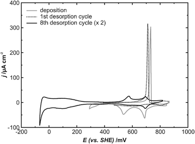 | ||
| Fig. 1 Cyclic voltammograms of Cu-modified Pt(111), dE/dt = 10 mV s−1, gray line: the deposition electrolyte (0.1 M HClO4 + 1 mM CuO), black lines: stripping of the Cu layer after exchange for the blank electrolyte (0.1 M HClO4). | ||
The measured charge density of (405 ± 25) μC cm−2 for the Cu desorption is about 15% less than expected for a pseudomorphic Cu monolayer, assuming a transfer of 2 electrons per Cu atom (480 μC cm−2). This lack of charge is known in the literature1,20 and denoted the coadsorption of anions during the Cu deposition. However, there is some disagreement concerning the charge value: whereas some ref. 1 and 20 report a value of 340 μC cm−2, a study of Marković et al.19 reports a dependence of the charge density on the Cu2+ concentration and quotes a value of 460 μC cm−2 for a 0.1 M HClO4 solution containing 1 mM Cu2+, which is very close to the ideally expected value.
STM images recorded at potentials around 400 mV, i.e. after Cu deposition, show atomically smooth and homogeneous terraces (Fig. 2a). On high resolution images an atomic structure with hexagonal symmetry is found (Fig. 2b), which exhibits a nearest neighbor distance of (2.77 ± 0.04) nm. The atomic structure both fits with the lattice of the Pt(111) surface and is in good agreement with previous LEED results,1,22 which proposed a (1 × 1) structure for the Cu UPD phase. However, STM images also show some defects within the Cu layer (Fig. 2b), which actually indicates a lower Cu coverage. The defects' fraction of the Cu layer can be estimated at 0.1 ML, however, due to their random distribution and different sizes this should be just considered as a rough value. Also their origin remains unclear, even high resolution STM images do not reveal any specific adsorbate within these defects. In either case, they may explain most of the apparently missing desorption charge.
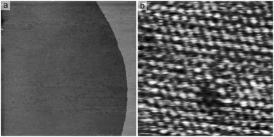 | ||
| Fig. 2 STM images of the Cu-covered Pt(111) electrode in the deposition electrolyte (0.1 M HClO4 + 1 mM CuO): (a) atomically flat morphology (552 nm)2, E = 375 mV, UB = 156 mV, IT = 1 nA; (b) defective (1 × 1)-structure (4.63 nm)2, E = 402 mV, UB = 1 mV, IT = 50 nA. | ||
It should also be mentioned that the previous discussion20 on the charge contribution of coadsorbed anions is based on a misinterpretation of the  structure found for a Cu submonolayer on Au(111) electrodes. This structure was revealed in later studies1,2,23 to be formed by 0.33 ML of coadsorbed HSO4− anions stabilizing a ΘCu = 0.66 ML Cu layer and not by a Cu layer with ΘCu = 0.33 ML.20
Summarizing this discussion, it appears likely that underpotential deposition of copper on Pt(111) surfaces yields to the formation of a pseudomorphic overlayer with some local defects. They are also the reason for the apparent lack of desorption charge in the CV curves, with respect to an ideal, i.e. defect-free, Cu-monolayer. However, the origin of these defects remains unclear, as STM images do not reveal any distinctive species within the defects. Based on these results, an actual Cu coverage of approximately 0.9 ML is assumed for the following, which forms a pseudomorphic (1 × 1)-structure on the Pt(111) surface.
3.2 Exchange for blank HClO4 solution
The Cu deposition is followed by an electrolyte exchange for a blank, i.e. Cu-free, 0.1 M HClO4 electrolyte, to prevent any further Cu deposition during the following experiments at lower potentials. This electrolyte exchange is carried out under potential control at a constant potential of 300 mV.Cyclic voltammograms obtained in the blank electrolyte (black curves in Fig. 1) show that no copper is lost during the electrolyte exchange: in the first anodic scan a sharp desorption peak still appears, for which the same charge density as in the Cu2+ containing deposition electrolyte is measured (dotted curve in Fig. 1). During the following cycles only a fraction of the dissolved Cu2+ cations are redeposited during the cathodic scan, leading to a continuous shrinking of the desorption peak with the number of cycles due to the virtually infinite dilution of Cu2+ into the blank electrolyte. After several potential cycles, the CV curve shows the characteristic hydrogen-UPD and OH−-adsorption features for Pt(111) electrodes24,25 but only a very small Cu desorption peak (black curve in Fig. 1).
In order to minimize the risk of any Cu dissolution, the potential was decreased by 150 mV prior to the STM measurements. STM images recorded after the electrolyte exchange show that the Cu layer remains unchanged on the surface. Large scale images still exhibit an atomically smooth and homogenous morphology (Fig. 3a), which also proves that all Cu2+ cations are removed from the liquid phase and no Cu bulk deposition occurs. On high resolution images, a (1 × 1) structure with some fuzzy defects is found (Fig. 3b), showing that also the pseudomorphic structure of the Cu layer is retained.
 | ||
| Fig. 3 STM images of the Cu-covered Pt(111) electrode after exchange for the blank electrolyte (0.1 M HClO4): (a) atomically flat morphology (499 nm)2, E = 199 mV, UB = 101 mV, IT = 1 nA; (b) (1 × 1)-structure with fuzzy defects (4.30 nm)2, E = 201 mV, UB = 3 mV, IT = 3 nA. | ||
3.3 Exposure of the Cu layer to CO
By performing a second electrolyte exchange for a CO-saturated 0.1 M HClO4 solution, the Cu-modified Pt(111) surface was finally subjected to CO. | ||
| Fig. 4 Morphology of the Cu layer after exposure to CO: (a) coalescent defect structure (534 nm)2, E = −50 mV, UB = 7 mV, IT = 10 nA; (b) partial diffusion into a 2nd Cu layer (108 nm)2, E = −42 mV, UB = 100 mV, IT = 1 nA; (c) line profile to (a); (d) line profile to (b). | ||
 | ||
| Fig. 5 Potentiodynamic STM images of the Cu dissolution in a CO-saturated 0.1 M HClO4 electrolyte, the scale in the STM images corresponds to the potential in the current–voltage curve in Fig. 6: (a) (349 nm)2, E = −49 mV to +547 mV, UB = 106 mV, IT = 3 nA; (b) (349 nm)2, E = 547 mV to 936 mV, UB = 106 mV, IT = 3 nA; (c), (d) line profiles to (a). | ||
The rearrangement of the Cu layer is driven by the formation of attractive Pt–CO bindings. Their higher binding strength compared to Pt–Cu bindings is known from previous studies: in the presence of CO, the UPD of copper on Pt(100)11 and Pt(111)10 electrodes vanishes. DFT calculations revealed a Pt(111)–CO binding energy of −1.5 eV, which is significantly more negative than the binding energy of CO to both, a pseudomorphic Cu layer on Pt(111) (−0.9 eV) and a pure Cu(111) surface (−0.6 eV).26 Energetically it should thus be favorable to replace all copper by CO, which, however, is not possible because the Cu layer is stabilized by the low electrode potential against anodic dissolution. Consequently, one would expect that the copper agglomerates into large clusters in order to maximize the area of the Pt(111) surface making contact with CO.
However, no continuing morphology changes of the Cu layer towards cluster formation can be observed in the following STM images, indicating a suppression of Cu diffusion, both over the Pt(111) surface and into a second layer, in agreement with previous results that the adsorption of CO strongly influences the activation barriers for diffusion on platinum.27 Hence, the newly formed defects do not originate from a long distance Cu mass transport, but from a local lateral compression of the initially pseudomorphic Cu layer to a more bulk-like structure. The diffusion into a second or a higher layer is only possible in the initial stage of the electrolyte exchange for the CO-saturated solution, while the CO concentration at the surface is still gradually increasing due to the limited flow-rate. Once the saturation concentration is reached (about 1–2 seconds) all further diffusion is suppressed. Consequently no evidence of an ongoing Cu diffusion can be found in STM images, such as a change in the Cu step edges to a more equilibrium shape or a growth of higher Cu islands.
Line profiles of the coalescent Cu islands exhibit a relative height of about 0.3 nm with respect to the CO-covered Pt(111) surface (Fig. 4c and d). This is significantly higher than for a pseudomorphic Cu film, for which one would expect a relative height of about 0.21 nm. Moreover, they appear even higher than the steps of the Pt(111) substrate (Fig. 4c). On the one hand this is due to the lateral compression of the Cu layer during CO adsorption, forcing Cu atoms to less ideal adsorption sites, e.g. on-top sites. On the other hand different materials exhibit different local densities of states due to which their relative height in STM images does not necessarily reflect the topological height difference. This may get even more pronounced in the presence of adsorbates, in particular in the case of different binding properties. However, for the second Cu layer a relative height of about 0.2 nm can be measured (Fig. 4d), which is within the expected range of Cu step heights, such as 0.21 nm for Cu(111) and 0.18 nm for Cu(100).
One of the rare cases of larger cluster-like Cu accumulations is shown in Fig. 5a. The Cu coverage in the vicinity of the clusters is reduced to about 0.6 ML. The clusters have a height of about 1.6 nm to 2.3 nm (Fig. 5c and d), roughly corresponding to 8 to 11 Cu layers. The total amount of copper in these clusters can thus be estimated at 0.6 ML in this image. Both the existence of the clusters and the locally different Cu coverage indicate that Cu diffusion has locally been possible during the electrolyte exchange. As these clusters are very rare, the reason for this locally enhanced diffusivity remains unclear.
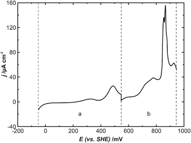 | ||
| Fig. 6 Current–voltage curve from −49 mV to +936 mV recorded simultaneously with STM images in Fig. 5, after which the potential was kept constant, dE/dt = 10 mV s−1, dashed lines: corresponding sections to the STM images (a/b), potential was kept constant in-between the images. | ||
These images reveal that the coalescent Cu layer remains unchanged up to a potential of about 550 mV (Fig. 5a). However, during the further potential increase to about 700 mV, it disappears completely from the Pt(111) surface (Fig. 5b). In contrast to the desorption in a CO-free solution (Fig. 1), the simultaneously recorded current–voltage curve does not show a sharp current spike in this particular potential range, which would indicate an oxidation of the Cu layer and thus explain directly its disappearance in the STM image (Fig. 6). It only shows a rather broad current wave at a potential of about 500 mV, where, however, the Cu layer remains unchanged in the STM image (Fig. 5a). Also the total anodic charge density during the potential increase to 700 mV, which can be estimated at (220 ± 50) μC cm−2, is significantly lower than that measured for the anodic desorption of the Cu layer in an Ar-saturated solution. Only upon further potential increase can a prominent current peak be observed at a potential of about 850 mV. This peak, however, is known in the literature for the oxidation of adsorbed CO on the Pt(111) surface.28,29 Moreover, the overall shape of the current–voltage curve, including the peaks at 500 mV and 750 mV, is in good agreement with that for a completely Cu-free system, i.e. a Pt(111) electrode in a CO-saturated 0.1 M HClO4 electrolyte.29
Accordingly, no feature in the current–voltage curve can be directly correlated with the oxidation and thus disappearance of the Cu film in STM-images, even though, for desorption, it has to be oxidized. However, it might be possible that either adsorption of CO on the previously Cu-covered regions of the Pt(111) electrode or the onset of bulk CO oxidation screens the charge transfer for the anodic Cu dissolution.
Also in the STM images the exact potential for the Cu desorption remains ambiguous. Although the Cu layer seems to disappear at a potential of about 700 mV, it may not necessarily desorb into the electrolyte. Alternatively the onset of the oxidation of CO, which stabilizes the coalescent structure of the Cu layer, might lower the barrier for Cu diffusion and thus trigger a phase transition to a mobile phase. Such a mobile phase may appear invisible for STM, yielding in atomically flat and apparently adsorbate free terraces. Thus it remains unclear whether the apparently adsorbate free terraces in the potential range between 700 mV and 850 mV (Fig. 5b) indicate Cu desorption. The only notable additional feature is a fuzzy depression suddenly appearing at a potential of about 850 mV (Fig. 5b). This feature is coincident with the CO oxidation peak in the current–voltage curve (Fig. 6). Thus it may correspond to some disturbances of the STM caused by the CO oxidation, or alternatively, it may also indicate the desorption of a mobile Cu-adlayer into the electrolyte.
In summary, both Cu desorption and CO oxidation cannot be considered as isolated processes; they appear rather related to each other and occur under very similar potential conditions. Even though STM images suggest a desorption potential of about 650 mV, it remains unclear whether it corresponds to an alternative transition to a mobile phase.
 | ||
| Fig. 7 (a) Atomically flat morphology of the Cu film after exposure to: (a) strong HER in Ar-saturated solution (517 nm)2, E = 350 mV, UB = 12 mV, IT = 20 nA; (b) a CO2-saturated electrolyte (513 nm)2, E = 208 mV, UB = 103 mV, IT = 10 nA. | ||
3.4 Exposure to a CO2 saturated solution
For CO2 an inverse binding situation with respect to CO can be assumed. Hence a morphology change of the Cu layer would be induced by Cu–CO2 rather than Pt–CO2 bindings.To investigate this situation, a second electrolyte exchange for a CO2-saturated 0.1 M HClO4 electrolyte was performed after preparation of the Cu layer. STM images recorded at a potential of about 200 mV exhibit that the morphology of the Cu film remains unchanged and atomically smooth (Fig. 7b). Hence, the Cu film is stabilized by the Pt(111) surface against CO2-induced morphological changes. Also, in agreement with the literature,30 no restructuring induced by attractive Pt–CO2 bindings can be found, in contrast to the results in a CO-saturated electrolyte. However, it has to be considered that copper is generally able to reduce CO2 to CO,13,14,16,17 which may eventually lead to the same morphology changes as is observed in a CO-saturated solution.
4 Conclusions
The UPD of copper on a Pt(111) electrode and the influence of CO and CO2 coadsorbates on the thus deposited Cu films have been studied by means of EC-STM. UPD leads to the formation of a Cu layer with a pseudomorphic (1 × 1) structure, in agreement with previous LEED studies. However, the Cu layer also contains some point defects, which naturally cannot be observed with LEED. Even though their origin remains unclear in STM images, they suggest an alternative understanding of the known, too low charge transfer during the Cu deposition: instead of a charge contribution from coadsorbed anions, the total Cu coverage is reduced by these defects.Exposure to CO leads to a rearrangement of the Cu layer from its initially pseudomorphic structure to a defective coalescent structure, which is driven by the formation of attractive Pt–CO bindings. CO also influences the anodic Cu dissolution: while the Cu layer apparently disappears in STM at a potential of about 650 mV, the simultaneously recorded current–voltage curve does not indicate any related anodic current and has virtually the same appearance as for a completely Cu-free system.
In contrast, exposure to CO2, which should bind more attractive to copper rather than platinum, does not yield rearrangement of the Cu layer. Obviously its binding to the Pt(111) surface stabilizes it against a CO2-induced restructuring. However, as CO2 may get reduced to CO over copper, a CO-induced restructuring of the Cu layer may occur after longer exposures.
Acknowledgements
The Danish National Research Foundations Center for Individual Nanoparticle Functionality (DNRF54) is gratefully acknowledged for funding.References
- E. Herrero, L. Buller and H. Abruna, Chem. Rev., 2001, 101, 1897–1930 CrossRef CAS PubMed.
- M. F. Toney, J. N. Howard, J. Richer, G. L. Borges, J. G. Gordon, O. R. Melroy, D. Yee and L. B. Sorensen, Phys. Rev. Lett., 1995, 75, 4472–4475 CrossRef CAS PubMed.
- N. Kimizuka and K. Itaya, Faraday Discuss., 1992, 94, 117–126 RSC.
- N. S. Marinkovic, J. X. Wang, J. S. Marinkovic and R. R. Adzic, J. Phys. Chem. B, 1998, 103, 139–144 CrossRef.
- J. Hotlos, O. Magnussen and R. Behm, Surf. Sci., 1995, 335, 129–144 CrossRef CAS.
- N. Hai, T. Huynh, A. Fluegel, M. Arnold, D. Mayer, W. Reckien, T. Bredow and P. Broekmann, Electrochim. Acta, 2012, 70, 286–295 CrossRef CAS.
- T. L. Wade, R. Vaidyanathan, U. Happek and J. L. Stickney, J. Electroanal. Chem., 2001, 500, 322 CrossRef CAS.
- K. Varazo, M. D. Lay, T. A. Sorenson and J. L. Stickney, J. Electroanal. Chem., 2002, 522, 104 CrossRef CAS.
- S. Kelemen, T. Fischer and J. Schwarz, Surf. Sci., 1979, 81, 440–450 CrossRef.
- C. Lucas, N. Marković and P. Ross, Surf. Sci., 2000, 448, 77–86 CrossRef CAS.
- C. Lucas, N. Marković, B. Grgur and P. Ross, Surf. Sci., 2000, 448, 65–76 CrossRef CAS.
- N. Schumacher, K. Andersson, L. Grabow, M. Mavrikakis, J. Nerlov and I. Chorkendorff, Surf. Sci., 2008, 602, 702–711 CrossRef CAS.
- Y. Hori, A. Murata, R. Takahashi and S. Suzuki, J. Am. Chem. Soc., 1987, 109, 5022–5023 CrossRef CAS.
- Y. Hori, R. Takahashi, Y. Yoshinami and A. Murata, J. Phys. Chem. B, 1997, 101, 7075–7081 CrossRef CAS.
- Y. Hori, Modern Aspects of Electrochemistry, Springer, New York, 2008, pp. 89–189 Search PubMed.
- A. A. Peterson, F. Abild-Pedersen, F. Studt, J. Rossmeisl and J. K. Nørskov, Energy Environ. Sci., 2010, 3, 1311–1315 CAS.
- W. Durand, A. Peterson, F. Studt, F. Abild-Pedersen and J. Nørskov, Surf. Sci., 2011, 605, 1354–1359 CrossRef CAS.
- M. Wilms, M. Kruft, G. Bermes and K. Wandelt, Rev. Sci. Instrum., 1999, 70, 3641–3650 CrossRef CAS.
- N. Marković and P. Ross, Langmuir, 1993, 9, 580–590 CrossRef.
- L.-W. Leung, T. Gregg and D. Wayne Goodman, Chem. Phys. Lett., 1992, 188, 467–470 CrossRef CAS.
- J. Greeley, Electrochim. Acta, 2010, 55, 5545–5550 CrossRef CAS.
- L.-W. Leung, T. Gregg and D. Wayne Goodman, Langmuir, 1991, 7, 3205–3210 CrossRef CAS.
- M. Nakamura, O. Endo, T. Ohta, M. Ito and Y. Yoda, Surf. Sci., 2002, 514, 227–233 CrossRef CAS.
- A. Berná, V. Climent and J. Feliu, Electrochem. Commun., 2007, 9, 2789–2794 CrossRef.
- A. Hitotsuyanagi, M. Nakamura and N. Hoshi, Electrochim. Acta, 2012, 82, 512–516 CrossRef CAS.
- M. Mavrikakis, B. Hammer and J. Nørskov, Phys. Rev. Lett., 1998, 81, 2819–2822 CrossRef.
- M. Kalff, G. Comsa and T. Michely, Phys. Rev. Lett., 1998, 81, 1255–1258 CrossRef CAS.
- N. Marković, B. Grgur, C. Lucas and P. Ross, J. Phys. Chem. B, 1999, 103, 487–495 CrossRef.
- J. Inukai, D. A. Tryk, T. Abe, M. Wakisaka, H. Uchida and M. Watanabe, J. Am. Chem. Soc., 2013, 135, 1476–1490 CrossRef CAS PubMed.
- N. Hoshi and Y. Hori, Electrochim. Acta, 2000, 45, 4263–4270 CrossRef CAS.
| This journal is © the Owner Societies 2013 |