 Open Access Article
 This Open Access Article is licensed under a
 Creative Commons Attribution 3.0 Unported Licence
Influence of graphene synthesizing techniques on the photocatalytic performance of graphene–TiO2 nanocomposites
Raja
Sellappan
*a,
Jie
Sun
b,
Augustinas
Galeckas
c,
Niclas
Lindvall
b,
August
Yurgens
b,
Andrej Yu.
Kuznetsov
c and
Dinko
Chakarov
a
aDepartment of Applied Physics, Chalmers University of Technology, Sweden. E-mail: rayas@chalmers.se; Tel: +46 76 332 3373
bDepartment of Microtechnology and Nanoscience, Chalmers University of Technology, Sweden
cDepartment of Physics/Centre for Materials Science and Nanotechnology, University of Oslo, P.O. Box 1126, Blindern, N-0318 Oslo, Norway
First published on 23rd July 2013
Abstract
Model photocatalysts composed of TiO2–graphene nanocomposites are prepared to address the effect of graphene quality on their photocatalytic performance. Graphene is synthesized by catalyst-assisted chemical vapor deposition (CVD), catalyst-free CVD and solution processing methods. TiO2 is prepared by reactive magnetron sputtering and subsequent annealing. Fabricated model photocatalysts have different morphology and physical properties, as revealed using spectrophotometry, atomic force microscopy, X-ray photoelectron spectroscopy, Raman spectroscopy, photoluminescence, and four-probe electrical measurements. All graphene-containing composites have significantly higher photocatalytic activity compared to bare TiO2 films in the gas phase methanol photooxidation tests. Their activity is proportional to the electrical conductivity and surface roughness of the respective carbon structure, which in turn depends on the preparation methods. The mechanisms of enhancement are further assessed by comparison with the performance of reference TiO2–graphitic-carbon and TiO2–Au thin films.
1. Introduction
Carbonaceous nanomaterials incorporated into TiO2 photocatalyst systems have made significant contributions to their photocatalytic enhancement owing to their favorable physical and electronic properties.1–6 A number of studies have demonstrated that incorporation of carbon allotropes into the TiO2 matrix greatly minimizes its inherent problems, such as limited light absorption (only in the UV region) and the fast recombination rate of photogenerated charge carriers.4,7–12 Much effort has recently been devoted to understanding mechanisms of charge carrier dynamics in nanocomposites containing carbon nanotubes (CNT's),13 graphite,14 and graphene.15–20 Recent results indicate that carbon in these composites has the ability to suppress charge carrier recombination of TiO2 through serving as an electron storage and/or conducting medium for the photogenerated electrons.15,21–27 Most of these studies have been focused on CNT's13,18,19 and less attention in terms of charge carrier dynamics has been paid to graphene.15–17Graphene is regarded as one of the rapidly emerging materials in catalysis3 and photocatalysis5 because of its unique properties such as theoretically high charge carrier mobility and surface area.28 It has been reported that graphene-containing nanocomposites contribute to improving the light absorption and the adsorption of reactants, and extending charge carrier lifetime of TiO2.5,29–33Graphene is currently synthesized using different methods,5,22,34–37 depending on the end application. The crystallinity of graphene, the number of defects, etc., obtained from different preparation techniques vary considerably. Charge carrier dynamics is strongly affected by crystal defects and surface morphology.38 It is believed that defect-rich graphene will hinder the charge carrier mobility and impede the probability of charge carrier separation in TiO2 based composite systems.
To the best of our knowledge, there are very few studies specially devoted to the effect of graphene quality on photocatalytic performance of TiO2.39 Here we design, fabricate, and evaluate model nanocomposites of graphene–TiO2 with the aim of understanding the role of graphene prepared using different techniques on the photocatalytic performance of TiO2. We adopt widely used methods such as chemical vapour deposition (CVD) and solution processing techniques to synthesize graphene. Special emphasis is given to surface morphology and electrical conductivity of graphene and their relationship with charge carrier dynamics. Finally, we compare photocatalytic activity of graphene–TiO2 composites with those of graphitic-carbon–TiO2 and gold film–TiO2 composites to examine the importance of electrical conductivity and interfacial contact.
2. Experimental sections
2.1. Sample fabrication
Substrates of 1 cm2 fused silica (University Wafer) were used for all compositions investigated. Standard cleaning with acetone and isopropyl alcohol was employed to remove organic residues from the substrates, which were then rinsed in de-ionized water and subsequently blow-dried in nitrogen gas. Oxygen plasma cleaning was carried out for 1 minute under 250 mbar at 50 W RF power prior to deposition.Graphene has been synthesized by three different well-known methods, two of which were employed and demonstrated in our previous work.35,36,40 The same recipes were used to synthesize graphene on a fused silica substrate. Some key parameters of the preparation conditions used in our previous works are briefly reviewed in what follows. The first synthesis method we used was catalyst-assisted growth of graphene by CVD.36 The deposition was carried out in a commercial system (Black Magic, AIXTRON Nanoinstruments Ltd), where copper foil was used as a catalyst as well as the substrate for the growth of graphene. The precursor for the reaction was argon diluted high purity methane (5% volume ratio). The foil was heated to 1000 °C with a 300 °C min−1 ramp rate. The flow rate of H2, Ar, and CH4 during the deposition was maintained at 20, 1000, and 30 SCCM, respectively. After growing graphene for 5 minutes on the copper foil, it was transferred to the fused silica substrate using PMMA polymer films to mechanically support graphene. We call this type of graphene as transferred graphene (TG).
The second method that we used was catalyst-free growth of graphene by CVD.35,40 As the name suggests, this method allows us to grow graphene directly on the fused silica substrate without catalysts. The deposition was performed in the same growth chamber at 1000 °C using 20, 1000, and 20 SCCM flows of H2, Ar, C2H2, respectively. The 20 minute growth time yields nominally single-layer graphene. By controlling the deposition time and the precursor concentration, the thickness can be tuned from monolayer graphene to thick graphite. We refer to this type of graphene as transfer-free graphene (TFG).
The third method was deposition of graphene by commercially available graphene oxide (GO) aqueous solution (Graphene Supermarket, 275 mg L−1, 0.5–5 μm, and 20% oxygen). This has been the most widely used method for preparing graphene–TiO2 nanocomposites.30–33,41 GO solution was spin coated on the fused silica at 750 rpm for one minute and subsequently baked at 100 °C for five minutes. The samples were then reduced in a nitrogen environment using thermal annealing at 200 °C for 15 minutes in a rapid thermal process (RTP) system. We refer to this type of graphene as reduced graphene oxide (RGO).
Carbon films were deposited at room temperature by e-beam evaporation (AVAC HVC600) with polycrystalline graphite as a source material. The deposition was performed under vacuum (typical pressure 1–3 × 10⁻⁶ mbar) with the deposition rate maintained at 1 Å s−1. The nominal thickness of the carbon films was 20 nm. Post-deposition annealing of carbon films at 800 °C in an argon atmosphere for 10 minutes in the RTP system transformed them to graphitic-carbon films.10 Gold thin films with thickness of 20 nm were prepared in a similar way in another e-beam evaporation system (Lesker PVD 225) with the deposition rate of 1 Å s−1.
TiO2 was prepared by DC reactive magnetron sputtering using a FHR MS150 system. The deposition was performed at room temperature with a base pressure of 5 × 10⁻³ mbar and 1 kW power. The flow rate of reactive oxygen was 12 SCCM during the oxidation of titanium target and reduced to 4 SCCM during the deposition. The thickness of the film was about 50 nm as confirmed by surface ellipsometry (J. A. Woollam M2000). Post-deposition annealing of TiO2 was carried out at 500 °C in an argon atmosphere for 10 minutes in the RTP system. This procedure led to formation of films with anatase structure.10
2.2. Characterization techniques
Optical measurements were carried out using a Cary Varian 5000 spectrophotometer in double beam mode. For surface topography characterization, we used a Bruker Dimension 3100 SPM in tapping mode. XPS measurements were performed in a PHI 5500 system at the base pressure of 10−10 mbar using a Mg Kα source. Sheet resistivity was measured with a four-probe system (CMT-SR2000N) using a probe with 1 mm pin spacing. Raman measurements were performed in a Horiba XploRa system using a 638 nm laser excitation source at RT. The Raman signal was collected using an Olympus 100× objective.For the photoluminescence measurements, we used a 325 nm wavelength radiation of He–Cd laser (cw) as an excitation source with an average power density of 3 W cm−2. The luminescence from the samples was collected by the microscope objective and analyzed using a fiber-optic spectrometer (Ocean Optics, usb4000).
Time-resolved photoluminescence measurements have been carried out at 10 K employing a 372 nm wavelength pulsed laser (PicoQuant, power 2 mW @ 40 MHz) as an excitation source. The selected spectral region of interest was filtered out from the total PL signal using imaging average registered by a photon counting system (Becker&Hickl, spectrograph (HORIBA Jobin Yvon, iHR320) and 50 ps-pulsed, PMC100, TCSPC, MCP) with an overall time resolution of ∼100 ps.
2.3. Photocatalytic tests
The photocatalytic performance of the composites was tested in a microreactor using gas phase methanol photooxidation as a model reaction. The reaction products were monitored by a quadrupole mass spectrophotometer (QMS) coupled directly to the reactor via a capillary. The source of illumination was a 100 W mercury arc lamp along with set of lenses and apertures. Photocatalytic performance of the composites was evaluated over the UV spectral range from 250 nm to 380 nm (Hoya U-340 filter) with a light intensity of about 350 mW cm−2. The reactor system was thermalized by circulating cooling water to avoid light induced heating.3. Results and discussion
The nanocomposite photocatalysts consist of TiO2 films deposited onto carbon (C) films of different structures. Unless otherwise mentioned, the term carbon films in the following discussion refer to graphene or graphitic carbon structures. It should be mentioned that most of the basic characterizations of the deposited carbon structure have comprehensively been carried out in our previous studies. We used them as reference to interpret some findings in the present work when needed.10,14,35,36,40Table 1 displays a summary of all prepared composites, performed characterizations, and main observations. The prepared nanocomposites are represented as Gx where x = 0 to 7 denotes different compositions as indicated in Table 1. These representations will be followed in the rest of the discussion.| Samples | Compositions | Average roughness of carbon and gold films (Ra) nm | Average roughness of TiO2 composites (Ra) nm | Sheet resistivity (KΩ □−1) | CO2 production rate with respect to bare TiO2 | PL quenching factor with respect to bare TiO2 |
|---|---|---|---|---|---|---|
| a Previous study.36 b Previous study.35 c Taken from ref. 42. | ||||||
| G0 | Bare TiO2 | 0.50 | — | 1.0 | 1.0 | |
| G1 | Transferred graphene (TG)–TiO2 | 0.68 | 0.89 | 0.5 to 1a | 5.5 | 1.5 |
| G2 | Transfer-free graphene (TFG)–TiO2 | 1.13 | 1.01 | 1.5 to 13b | 2.8 | 1.25 |
| G3 | Reduced graphene oxide (RGO)–TiO2 | 0.53 | 0.65 | 40 to 100c | 2.05 | 1.25 |
| G4 | Graphene oxide (GO)–TiO2 | 0.73 | 0.7 | — | 1.8 | 1.01 |
| G5 | Graphitic-carbon (GC)–TiO2 | 0.49 | 0.77 | 1.5 | 11 | 2.04 |
| G6 | Ti–GC–TiO2 | 0.6 | 1.1 | 0.8 | 12.8 | 2.15 |
| G7 | Au–TiO2 | 0.4 | 0.6 | 0.0025 | 1.25 | — |
3.1. Optical characterization
Fig. 1 shows optical transmission spectra of graphene prepared by different synthesizing techniques. The optical transmission of G1 is between 97 and 98% in the visible range. It has a dip at the 270 nm wavelength due to exciton-shifted Van Hove singularity in the graphene density of states.43 The 2 to 3% optical absorption in the visible range is typical for the nominal monolayer graphene as reported in several studies.22,44–46 The dip in the UV region is slightly red shifted and the visible light transmission is decreased for G2 (TFG) and several layer graphite. The slight redshift and decrease in visible light transmission is due to narrowing of π bands and increasing thickness of graphene layers that modifies the electronic band structure. For the solution-processed sample (G4), the dip was at ∼240 nm similarly to the observations reported in the literature.45 The dip was shifted to 270 nm for G3 (RGO) after the thermal reduction in a nitrogen atmosphere. In addition, the visible light transmission of G3 is relatively lower compared to G4. This is interpreted as restoring of conjugated sp2 networks after the thermal treatment. The optical transmission of G3 (RGO) is more or less the same as that of the sample G1 (TG), implying that the thickness of both samples is roughly the same and mostly consists of monolayer sheets. Upon deposition of TiO2, the optical transmission of the composites is nearly the same for all graphene samples due to the large thickness of TiO2 films compared to the graphene layer thickness. In other words, the optical transmission of composites is limited by the transmission of bare TiO2.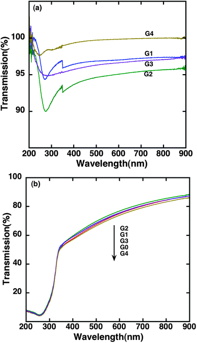 | ||
| Fig. 1 Optical transmission spectra of (a) Graphene films prepared by different methods. The small step seen at 350 nm is due to the lamp changeover in the instrument. (b) Respective TiO2–graphene composites. | ||
3.2. Photocatalytic performance tests
Methanol photooxidation is an appropriate test for assessing the catalytic performance of prepared nanocomposites. It is one of the widely used model reactions,47–49 where methanol and oxygen react at the surface of TiO2 under UV illumination producing carbon dioxide and water: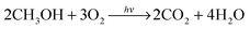 | (1) |
 | ||
| Fig. 2 Normalized CO2 production rates of TiO2 composites with different compositions obtained from the methanol photooxidation test. The dotted line represents the activity of bare TiO2 (G0). | ||
3.3. Morphological characterization
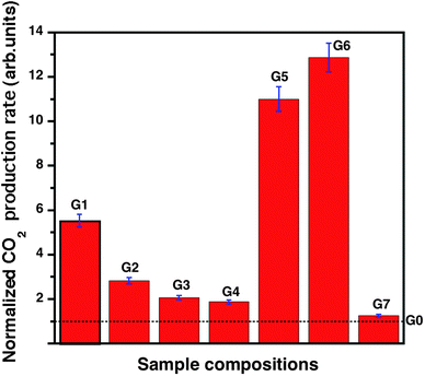
The surface topography of carbon films and TiO2 composites is shown in Fig. 3(a and b). We used the average surface roughness (Ra), determined from AFM, as a parameter to assess the surface morphology. Obtained Ra values are quoted in Table 1. Different synthesizing techniques of graphene have given rise to different Ra values even though the substrate for all composites is the same. This is attributed to the difference in reaction conditions such as precursors, flow rate, deposition time, etc. | ||
| Fig. 3 Tapping mode AFM images of (a) Carbon films prepared by different methods. The scan size is 5 μm × 5 μm. (b) TiO2 composite of different compositions. The scan size is 1 μm × 1 μm. See Table 1 for details. | ||
The samples G1 (TG) and G3 (RGO) have lower surface roughness compared to the sample G4 (GO). The lower surface roughness of G1 and G3 indicates that the graphene flakes are homogenous and more or less uniformly distributed throughout the substrate. The sample G1 has high-quality, uniform monolayer graphene with carrier mobility on the order of 103 cm2 V−1 s−1.36 However, transferring such graphene from the copper foil to fused silica introduced some wrinkles and strains. We also noticed some residues of PMMA on graphene after the transfer. On the other hand, the sample G3 (RGO) has no such issues of polymer residues, but the graphene flakes are not uniform as the sample G1 (TG). Moreover, its purity is lower than that of the sample G1 since, according to the XPS measurements (Fig. 4), there are still some hydroxyl and epoxy groups present after the gentle reduction. This is seen in Fig. 4(b), where we note the substantial decrease of C–O (286.6 eV) and C![[double bond, length as m-dash]](https://www.rsc.org/images/entities/char_e001.gif) O (287.8 eV) peaks and increase of C–C (284.6 eV)50,51 peak intensity after the thermal reduction. We interpret this as the restoring of sp2-domains in G3. The peak at 282.3 eV for GO is due to some impurities during the fabrication, which is not observed after the thermal reduction. The slightly higher surface roughness of the sample G4 (GO) was due to the presence of more oxygen (and other functional) groups in the layer. It has been demonstrated in our previous studies that samples of G2 type are predominantly composed of sp2 nanocrystallites with dimensions on the order of 10 nm and containing more grain boundaries.35 It turns out to be the reason for the increased surface roughness of G2 compared to others. On the other hand, graphitic-carbon and gold films have lower surface roughness, suggesting that the surface of the carbon films is uniform. For graphitic carbon films we observed small flakes, which confirm that the evaporated carbon films are composed of nanocrystalline flakes. Comparing the Ra value of graphene composites after the deposition of TiO2, the difference is approximately the same as that of a bare graphene layer, indicating the influence of underlayer on the growth of TiO2.
O (287.8 eV) peaks and increase of C–C (284.6 eV)50,51 peak intensity after the thermal reduction. We interpret this as the restoring of sp2-domains in G3. The peak at 282.3 eV for GO is due to some impurities during the fabrication, which is not observed after the thermal reduction. The slightly higher surface roughness of the sample G4 (GO) was due to the presence of more oxygen (and other functional) groups in the layer. It has been demonstrated in our previous studies that samples of G2 type are predominantly composed of sp2 nanocrystallites with dimensions on the order of 10 nm and containing more grain boundaries.35 It turns out to be the reason for the increased surface roughness of G2 compared to others. On the other hand, graphitic-carbon and gold films have lower surface roughness, suggesting that the surface of the carbon films is uniform. For graphitic carbon films we observed small flakes, which confirm that the evaporated carbon films are composed of nanocrystalline flakes. Comparing the Ra value of graphene composites after the deposition of TiO2, the difference is approximately the same as that of a bare graphene layer, indicating the influence of underlayer on the growth of TiO2.
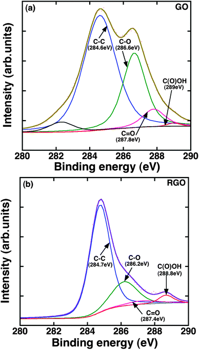 | ||
| Fig. 4 XPS spectra in the C1s region of (a) G4 (GO) and (b) G3 (RGO). | ||
3.4. Raman characterization
Raman spectra of graphene prepared by different methods are shown in Fig. 5. The Raman spectra of the prepared graphene samples consist of the so-called D-, G-, and 2D-peaks. The observed Raman peaks are well-resolved and their peak positions are shown in Table 2. The D-peak is due to breathing modes of sp2 rings and its intensity is related to the amount of defects in the lattice. The G-peak is related to stretching modes of C–C bonds in the sp2 rings. The 2D-peak is the second order of the D-peak, which is due to zone-boundary phonons.52 The G and 2D peaks are the Raman signatures of the sp2-bonded networks in the material.53 The D-peak intensity of the sample G1 is the smallest, which is probably originating from the edges, compared to other graphene samples. The smaller D-peak indicates fewer defects in G1. In other words, the quality of G1 is the highest. The Raman spectra of the sample G3 (RGO) and G4 (GO) show well-resolved D- and G-peaks and smaller 2D peak intensity (shown clearly in the inset of Fig. 5). The relative intensity ratio of ID/IG is slightly higher for G3 than for G4, implying qualitatively the restoring of a number of sp2 graphitic domains with smaller crystallite sizes54 in G3 after the gentle thermal reduction in the nitrogen atmosphere. The Raman measurements of G3 and G4 are consistent with the XPS measurements. The Raman spectrum of the sample G2 shows a relatively higher ID/IG ratio as compared to G3 and G4, indicating that the quality of the material is higher than G3 and G4 but lower than G1.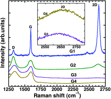 | ||
| Fig. 5 Raman spectra of graphene films prepared by different methods. The inset shows the 2D peak of G3 and G4. | ||
| Samples | D (cm−1) | G (cm−1) | 2D (cm−1) |
|---|---|---|---|
| G1 | 1328 | 1595 | 2648 |
| G2 | 1324 | 1592 | 2641 |
| G3 | 1340 | 1596 | 2640 |
| G4 | 1346 | 1600 | 2660 |
3.5. Electrical characterization
The sheet resistivity can be regarded as a measure of the electrical properties of graphene prepared by different synthesizing techniques. The measured values are reported in Table 1. As can be seen in Table 1, the sheet resistivity of G1 is the lowest among all carbon films. The result suggests that the quality of graphene prepared by catalyst-assisted growth renders fewer defects in the layer due to fewer grain boundaries as supported by the Raman results. The sample G2 has higher resistivity compared to G1. This implies that G2 contains more grain boundaries (see Fig. 3(a)), leading to higher resistivity due to increased scattering of charge carriers. We have estimated the sheet resistivity of G3 to be in the range between 40 and 100 KΩ □−1, since we used essentially the same reduction procedure as that described in ref. 42.On the other hand, the sheet resistivity of G5 and G6 is quite comparable to that of G1. It indicates that individual graphene sheets in graphite are of the same quality as G1. We noticed that titanium adhesion layer (thickness of ∼3 nm) in G6 reduces the resistivity by almost 2 times as compared to G5. In other words, the titanium layer promotes graphitization by acting as a catalyst. It should also be pointed out that graphitic-carbon produced by the e-beam evaporation has no residues of PMMA as found in G1; so the graphitic-carbon is free from residues or impurities. The resistivity of gold films was the lowest among all prepared composites.
3.6. Charge carrier dynamics
Fig. 6 shows PL spectra of all nanocomposites obtained at room temperature. The origin of the characteristic wide PL band in the visible region is commonly attributed to radiative recombination of self-trapped excitons in TiO2.55–57 It is immediately noticeable in Fig. 6 that the luminescence efficiency of the composites is generally lower compared to bare TiO2 films. To quantify these differences, the quenching factor for each case was established by weighting the integrated PL intensity over the 450 nm to 900 nm range against that from TiO2. The PL quenching factor is summarized in Table 1. The observed dissimilarities in the PL quenching factor of the composites can be inferred to different degrees of non-radiative charge carrier leakage at interfaces among other possible reasons reported in our previous study.14 As can be seen in Table 1, the PL quenching factor is considerably varied among composites and, in fact, is quite consistent with the trend in the photocatalytic enhancement factor. We were particularly interested in elucidating the difference between the two approaches used in the synthesis of graphene by CVD techniques, including assessment of one of the key material parameters such as charge carrier lifetime. For this purpose, we performed TRPL measurements at 10 K on samples G1 and G2 with G0 acting as a reference (see Fig. 7).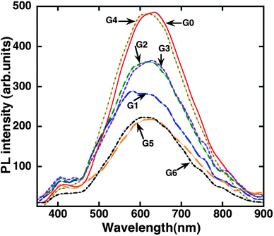 | ||
| Fig. 6 Room temperature PL spectra of composites prepared by different methods. The spectra have been smoothed in order to reduce noise. | ||
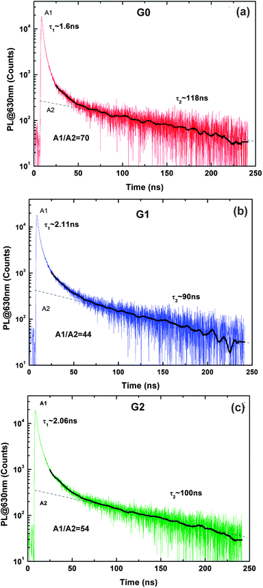 | ||
| Fig. 7 TRPL spectra obtained at 10 K for (a) G0, (b) G1 and (c) G2. The black solid line shows the curve fitting. The A1/A2 denotes the ratio of fast and slow decay components. | ||
In general, PL decay transients are non-exponential in TiO2. However, for the sake of convenience, the recombination kinetics is commonly approximated by introducing two parameters, the fast and slow time constants. In our previous study, we have comprehensively described the origin of different lifetime constants in TiO2 and their implications in the enhanced photocatalytic performance.14 The estimated minority charge carrier lifetimes of G0, G1, G2 are 118 ns, 90 ns, and 100 ns, respectively. We attribute the effect of shorter lifetimes in composites as compared to bare TiO2 preferably to improved transfer of the photogenerated electrons from TiO2 to graphene layer at the interface. The mutual PL intensity ratio of the fast and slow decay components (marked correspondingly as A1/A2 on the plots in Fig. 7) is a common measure of the roles of non-radiative versus radiative processes in the overall recombination. In this context, the lower ratio observed for the sample G1 (A1/A2 = 44), representing the TG, compared to that of G2 (A1/A2 = 54), representing the TFG, is indicative of G1 having fewer defects which increases non-radiative transfer of charge carriers. On the other hand, fewer defects in graphene imply relatively good electrical conductivity and that was measured for G1 over G2. We have pointed out in our previous study35 as well that the sample G2 has nanocrystalline graphene flakes with more grain boundaries, which act as scattering centers and lead to lower conductivity.
3.7. Photocatalytic mechanism
The driving force for the photocatalytic enhancement of composites is the increased charge carrier separation rate at the TiO2 and carbon interface. The process is illustrated in Fig. 8(a). Under the bandgap excitation of TiO2 with UV light, the photogenerated electrons are transferred to the carbon films whereas the holes are moved to the TiO2–gas interface where they will eventually react with methanol molecules. In order to avoid charging effects, the electrons should be leaked away from the carbon film and react with oxygen in the reactant mixture. The probability of charge carrier separation is strongly dependent on (i) band bending and formation of Schottky barrier (ii) electrical conductivity of the underlying layer and (iii) extent of the interfacial area. Accordingly, high activity should be expected for a sample with a large interfacial area, high electrical conductivity, and high Schottky barrier. We analyze the role of these parameters below.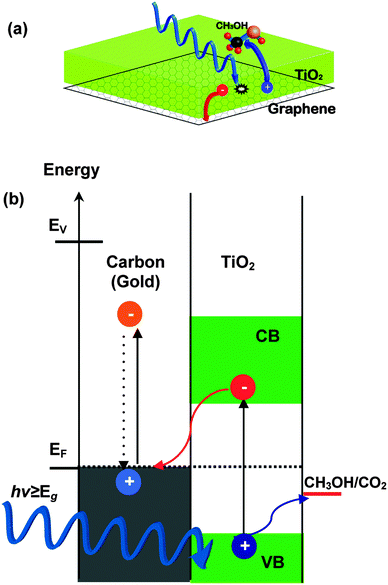 | ||
| Fig. 8 (a) Cartoon representation of the charge separation in TiO2–carbon composites under UV irradiation and photoreaction with CH3OH. (b) Energy level diagram at TiO2/carbon (gold) interface and the charge transfer under UV illumination. Note the fast e–h recombination in the carbon (gold) films. | ||
The work function of graphene, graphite, gold, and TiO2 is ∼4.48 to 4.6,58 4.659 to 4.8,60–62 5.353,63 and 4.2141 eV, respectively. Based on these values, the estimated magnitude of the Schottky barrier is highest for gold, followed by graphite and graphene. A higher Schottky barrier implies, according to Fig. 8(b) quicker charge carrier separation, suggesting the highest activity for the Au sample (G7). Similarly, the Au film has the lowest sheet resistivity, indicating that the gold sample should be the most active. However, contrary to these expectations, the photocatalytic enhancement factor of G7 is not the highest. What distinguishes the gold sample from the others is its smoothness. Therefore, we suggest that the surface roughness (or interfacial area) plays an equally important role as the film conductivity and the height of the Schottky barrier. It should be pointed out that rough gold films improve the photoactivity of TiO2, while nanometer small isolated gold particles embedded in TiO2 markedly boost the activity by two orders of magnitude (not shown).
The higher photoactivity observed for G5 and G6 (graphitic-carbon based nanocomposites) compared to G1–G4 (graphene-based) is attributed to the slightly higher Schottky barrier, lower electrical resistivity, and slightly larger surface area of the respective composites. Considering only graphene composites (assumed same Schottky barrier), the sample G1 shows the highest photoactivity, followed by G2 and G3, an order that follows the electrical conductivity of the samples. The same trend is observed for the PL quenching factor as well. It is the highest for G1 and followed by G2, G3, and G4. These conclusions can be further supported by the Raman measurements and the surface morphologies of the respective graphene samples, since they follow (almost) the same trends. It should be noted that there is a trade-off between the interface morphology and the electrical conductivity of G1 and G2 because the surface morphology of G2 is higher than G1 whereas the electrical conductivity is lower than G1.
It has recently been reported that carbon nanotubes have the capability of storing one electron per 32 carbon atoms in their conjugated sp2 networks.21 The electron storage in such carbon nanostructures, especially fullerenes, is related to pentagonal defects in their graphitic structure and large array of carbon–carbon double bonds in their network.21,64 Since the basic building block of a carbon nanotube is graphene, we would assume that both graphite and graphene prepared in this work may have the similar tendency of storing electrons in their conjugated sp2 networks as well. However it is not clearly understood yet as to what extent the dimensionality factor (or the density of electronic states at the Fermi level) would affect the electron trapping. Nevertheless, the tendency of electron trapping in both graphite and graphene can be qualitatively explained by PL findings. The PL quenching factor for graphitic carbon is higher than for graphene indicating that there is reduced recombination in the former material. Although the reduced recombination could indicate several possibilities, we interpret this as the enhanced photogenerated electrons transfer and subsequent trapping of the electrons in graphitic-carbon films. It is also noted that graphitic-carbon films with the titanium adhesive layer (G7) exhibit the highest photoactivity. The reason is that these samples possess both higher electrical conductivity and surface roughness, compared to graphitic-carbon films with no adhesion layer (G6).
4. Conclusions
We have found that morphology and electrical properties of graphene prepared by different methods differed substantially. By using the test reaction of gas phase methanol photooxidation, we evaluated the influence of these differences on the photocatalytic activity of TiO2–graphene composites. While all composites exhibited strongly enhanced activity compared to the activity of the bare TiO2 photocatalyst, the effect was proportional to the electrical conductivity and surface roughness of the respective carbon structure, which in turn was dependent on the preparation methods. The highest photocatalytic activity was obtained for the catalysis-assisted CVD graphene in comparison to the catalyst-free CVD and the solution-processed graphene samples. The enhancement was attributed to an improved charge separation at the interface between TiO2–graphene. We demonstrated by TRPL measurements that the charge carrier dynamics was faster in samples with lower resistivity and larger interfacial contact area. The conclusions were further supported by comparison with graphitic-carbon and gold-based TiO2 nanocomposites. The investigated systems could be used as models for future studies for improved synthesis and optimization of photocatalysts based on carbon–semiconductor composites.Acknowledgements
This work was supported by NER through project 52-N-I-S-F-D.References
- D. Eder and A. H. Windle, Adv. Mater, 2008, 20, 1787–1793 CrossRef CAS.
- R. Leary and A. Westwood, Carbon, 2011, 49, 741–772 CrossRef CAS.
- B. F. Machado and P. Serp, Catal. Sci. Technol., 2012, 2, 54–75 CAS.
- K. Woan, G. Pyrgiotakis and W. Sigmund, Adv. Mater., 2009, 21, 2233–2239 CrossRef CAS.
- Q. J. Xiang, J. G. Yu and M. Jaroniec, Chem. Soc. Rev., 2012, 41, 782–796 RSC.
- Y. H. Ng, S. Ikeda, M. Matsumura and R. Amal, Energy Environ. Sci., 2012, 5, 9307–9318 CAS.
- G. M. An, W. H. Ma, Z. Y. Sun, Z. M. Liu, B. X. Han, S. D. Miao, Z. J. Miao and K. L. Ding, Carbon, 2007, 45, 1795–1801 CrossRef CAS.
- S. U. M. Khan, M. Al-Shahry and W. B. Ingler, Science, 2002, 297, 2243–2245 CrossRef CAS.
- J. H. Park, S. Kim and A. J. Bard, Nano Lett., 2006, 6, 24–28 CrossRef CAS.
- R. Sellappan, J. F. Zhu, H. Fredriksson, R. S. Martins, M. Zach and D. Chakarov, J. Mol. Catal. A: Chem., 2011, 335, 136–144 CrossRef CAS.
- B. Tryba, A. W. Morawski and M. Inagaki, Appl. Catal., B, 2003, 41, 427–433 CrossRef CAS.
- H. Wang, X. Quan, H. T. Yu and S. Chen, Carbon, 2008, 46, 1126–1132 CrossRef CAS.
- Y. Yao, G. Li, S. Ciston, R. M. Lueptow and K. A. Gray, Environ. Sci. Technol., 2008, 42, 4952–4957 CrossRef CAS.
- R. Sellappan, A. Galeckas, V. Venkatachalapathy, A. Y. Kuznetsov and D. Chakarov, Appl. Catal., B, 2011, 106, 337–342 CrossRef CAS.
- S. Krishnamurthy, I. V. Lightcap and P. V. Kamat, J. Photochem. Photobiol., A, 2011, 221, 214–219 CrossRef CAS.
- N. J. Bell, H. N. Yun, A. J. Du, H. Coster, S. C. Smith and R. Amal, J. Phys. Chem. C, 2011, 115, 6004–6009 CAS.
- Y. H. Ng, I. V. Lightcap, K. Goodwin, M. Matsumura and P. V. Kamat, J. Phys. Chem. Lett., 2010, 1, 2222–2227 CrossRef CAS.
- Y. T. Liang, B. K. Vijayan, O. Lyandres, K. A. Gray and M. C. Hersam, J. Phys. Chem. Lett., 2012, 3, 1760–1765 CrossRef CAS.
- W. Q. Fan, Q. H. Lai, Q. H. Zhang and Y. Wang, J. Phys. Chem. C, 2011, 115, 10694–10701 CAS.
- Y. Y. Liang, H. L. Wang, H. S. Casalongue, Z. Chen and H. J. Dai, Nano Res., 2010, 3, 701–705 CrossRef CAS.
- A. Kongkanand and P. V. Kamat, ACS Nano, 2007, 1, 13–21 CrossRef CAS.
- Y. W. Zhu, S. Murali, W. W. Cai, X. S. Li, J. W. Suk, J. R. Potts and R. S. Ruoff, Adv. Mater., 2010, 22, 5226 CrossRef CAS.
- J. G. Yu, T. T. Ma and S. W. Liu, Phys. Chem. Chem. Phys., 2011, 13, 3491–3501 RSC.
- Q. J. Xiang, J. G. Yu and M. Jaroniec, Nanoscale, 2011, 3, 3670–3678 RSC.
- Q. J. Xiang, J. G. Yu and M. Jaroniec, J. Am. Chem. Soc., 2012, 134, 6575–6578 CrossRef CAS.
- Q. J. Xiang and J. G. Yu, J. Phys. Chem. Lett., 2013, 4, 753–759 CrossRef CAS.
- W. G. Wang, J. G. Yu, Q. J. Xiang and B. Cheng, Appl. Catal., B, 2012, 119, 109–116 CrossRef.
- A. K. Geim and K. S. Novoselov, Nat. Mater., 2007, 6, 183–191 CrossRef CAS.
- B. J. Jiang, C. G. Tian, Q. J. Pan, Z. Jiang, J. Q. Wang, W. S. Yan and H. G. Fu, J. Phys. Chem. C, 2011, 115, 23718–23725 CAS.
- H. Zhang, X. J. Lv, Y. M. Li, Y. Wang and J. H. Li, ACS Nano, 2010, 4, 380–386 CrossRef CAS.
- Y. H. Zhang, Z. R. Tang, X. Fu and Y. J. Xu, ACS Nano, 2011, 5, 7426–7435 CrossRef CAS.
- Y. H. Zhang, Z. R. Tang, X. Z. Fu and Y. J. Xu, ACS Nano, 2010, 4, 7303–7314 CrossRef CAS.
- Y. H. Zhang, N. Zhang, Z. R. Tang and Y. J. Xu, Phys. Chem. Chem. Phys., 2012, 14, 9167–9175 RSC.
- V. Singh, D. Joung, L. Zhai, S. Das, S. I. Khondaker and S. Seal, Prog. Mater. Sci., 2011, 56, 1178–1271 CrossRef CAS.
- J. Sun, M. T. Cole, N. Lindvall, K. B. K. Teo and A. Yurgens, Appl. Phys. Lett., 2012, 100, 022102 CrossRef.
- J. Sun, N. Lindvall, M. T. Cole, K. T. T. Angel, T. Wang, K. B. K. Teo, D. H. C. Chua, J. H. Liu and A. Yurgens, IEEE Trans. Nanotechnol., 2012, 11, 255–260 CrossRef.
- W. S. Hummers and R. E. Offeman, J. Am. Chem. Soc., 1958, 80, 1339 CrossRef CAS.
- M. R. Hoffmann, S. T. Martin, W. Y. Choi and D. W. Bahnemann, Chem. Rev., 1995, 95, 69–96 CrossRef CAS.
- Y. T. Liang, B. K. Vijayan, K. A. Gray and M. C. Hersam, Nano Lett., 2011, 11, 2865–2870 CrossRef CAS.
- J. Sun, N. Lindvall, M. T. Cole, K. B. K. Teo and A. Yurgens, Appl. Phys. Lett., 2011, 98, 252107 CrossRef.
- K. F. Zhou, Y. H. Zhu, X. L. Yang, X. Jiang and C. Z. Li, New J. Chem., 2011, 35, 353–359 RSC.
- G. Eda, G. Fanchini and M. Chhowalla, Nat. Nanotechnol., 2008, 3, 270–274 CrossRef CAS.
- F. Bonaccorso, Z. Sun, T. Hasan and A. C. Ferrari, Nat. Photonics, 2010, 4, 611–622 CrossRef CAS.
- V. G. Kravets, A. N. Grigorenko, R. R. Nair, P. Blake, S. Anissimova, K. S. Novoselov and A. K. Geim, Phys. Rev. B: Condens. Matter Mater. Phys., 2010, 81, 155413 CrossRef.
- D. Li, M. B. Muller, S. Gilje, R. B. Kaner and G. G. Wallace, Nat. Nanotechnol., 2008, 3, 101–105 CrossRef CAS.
- R. R. Nair, P. Blake, A. N. Grigorenko, K. S. Novoselov, T. J. Booth, T. Stauber, N. M. R. Peres and A. K. Geim, Science, 2008, 320, 1308 CrossRef CAS.
- W. Balcerski, S. Y. Ryu and M. R. Hoffmann, Int. J. Photoenergy, 2008, 964721 Search PubMed.
- O. I. Micic, Y. N. Zhang, K. R. Cromack, A. D. Trifunac and M. C. Thurnauer, J. Phys. Chem., 1993, 97, 13284–13288 CrossRef CAS.
- D. A. Panayotov, S. P. Burrows and J. R. Morris, J. Phys. Chem. C, 2012, 116, 6623–6635 CAS.
- H. A. Becerril, J. Mao, Z. Liu, R. M. Stoltenberg, Z. Bao and Y. Chen, ACS Nano, 2008, 2, 463–470 CrossRef CAS.
- S. F. Pei and H. M. Cheng, Carbon, 2012, 50, 3210–3228 CrossRef CAS.
- A. C. Ferrari, J. C. Meyer, V. Scardaci, C. Casiraghi, M. Lazzeri, F. Mauri, S. Piscanec, D. Jiang, K. S. Novoselov, S. Roth and A. K. Geim, Phys. Rev. Lett., 2006, 97, 187401 CrossRef CAS.
- M. S. Dresselhaus, A. Jorio, M. Hofmann, G. Dresselhaus and R. Saito, Nano Lett., 2010, 10, 751–758 CrossRef CAS.
- S. Stankovich, D. A. Dikin, R. D. Piner, K. A. Kohlhaas, A. Kleinhammes, Y. Jia, Y. Wu, S. T. Nguyen and R. S. Ruoff, Carbon, 2007, 45, 1558–1565 CrossRef CAS.
- N. D. Abazovic, M. I. Comor, M. D. Dramicanin, D. J. Jovanovic, S. P. Ahrenkiel and J. M. Nedeljkovic, J. Phys. Chem. B, 2006, 110, 25366–25370 CrossRef CAS.
- V. Melnyk, V. Shymanovska, G. Puchkovska, T. Bezrodna and G. Klishevich, J. Mol. Struct., 2005, 744, 573–576 CrossRef.
- H. Tang, H. Berger, P. E. Schmid, F. Levy and G. Burri, Solid State Commun., 1993, 87, 847–850 CrossRef CAS.
- G. Giovannetti, P. A. Khomyakov, G. Brocks, V. M. Karpan, J. van den Brink and P. J. Kelly, Phys. Rev. Lett., 2008, 101, 026803 CrossRef CAS.
- T. Takahashi, H. Tokailin and T. Sagawa, Phys. Rev. B: Condens. Matter Mater. Phys., 1985, 32, 8317–8324 CrossRef CAS.
- J. J. Zhao, J. Han and J. P. Lu, Phys. Rev. B: Condens. Matter Mater. Phys., 2002, 65, 193401 CrossRef.
- Y. J. Yu, Y. Zhao, S. Ryu, L. E. Brus, K. S. Kim and P. Kim, Nano Lett., 2009, 9, 3430–3434 CrossRef CAS.
- M. Shiraishi and M. Ata, Carbon, 2001, 39, 1913–1917 CrossRef CAS.
- A. Hölzel and F. K. Schulte, Solid Surface Physics, 1979, 85, pp. 1–150 Search PubMed.
- P. W. Fowler and A. Ceulemans, J. Phys. Chem., 1995, 99, 508–510 CrossRef CAS.
| This journal is © the Owner Societies 2013 |