 Open Access Article
 This Open Access Article is licensed under a Creative Commons Attribution-Non Commercial 3.0 Unported Licence
Electronic structure and morphology of dark oxides on zinc generated by electrochemical treatment†
Ying
Chen‡
ab,
Paul
Schneider
a,
Bi-Ju
Liu
c,
Sergiy
Borodin
a,
Bin
Ren
c and
Andreas
Erbe
*a
aMax-Planck-Institut für Eisenforschung GmbH, Max-Planck-Str. 1, 40237 Düsseldorf, Germany. E-mail: a.erbe@mpie.de; aerbe@arcor.de; Fax: +49 211 6792218; Tel: +49 211 6792890
bCenter for Electrochemical Sciences, Ruhr-Universität Bochum, Universitätstr. 150, 44780 Bochum, Germany
cState Key Laboratory of Physical Chemistry of Solid Surfaces and Department of Chemistry, College of Chemistry and Chemical Engineering, Xiamen University, Xiamen 361005, China
First published on 24th April 2013
Abstract
Oxides formed by electrochemical treatment of metals frequently have properties and structures very different from the respective bulk oxides. Here, electronic structure and chemical composition were investigated for the oxide formed on polycrystalline zinc after electrochemical oxidation, and after subsequent reduction, in a Na2CO3 electrolyte. Photoluminescence and spectroscopic ellipsometry show the presence of states deep in the ZnO band gap in the oxidized sample, which consists of a highly disordered oxide. These states determine the absorption of light in the visible spectral range. After reduction, the characteristics of the ZnO electronic structure have disappeared, leaving a defect-dominated material with a band gap of ∼1.8 eV. Complementary detailed analysis of the morphology of the resulting surfaces shows hexagon-shaped metallic Zn-“nanoplates” to be formed in the reduction step. The optical appearance of the surfaces is dark, because of their efficient extinction of light over a large part of the visible spectrum. The optical appearance is a result of changed surface morphology and electronic structure of the oxide film. Such materials may possess interesting applications in photocatalysis or photoelectrochemistry.
1 Introduction
Zinc oxide and ZnO-based materials are currently widely investigated semiconducting materials.1,2 One reason for their popularity are their optoelectronic properties.2–5 On the chemical side, photocatalytic and photoelectrocatalytic properties of ZnO receive tremendous attention.2,6–8 The electronic structure of the materials is crucial for their performance as photo(electro)catalysts. As the ZnO band gap is ∼3.4 eV, light absorption is strong only in the ultraviolet range of the spectrum. To achieve light absorption in the visible spectral range, sensitisation approaches have been used.2,6,7 Besides using more complex conjugated structures with light absorbing particles or molecules, defect-related intragap states can be used to enhance visible light absorption, thus catalytic activity.9,10 The role of these defect-related intragap states in the ZnO electronic structure has been studied for free ZnO.1,2,9,10ZnO-based corrosion products form naturally on metallic Zn, which is widely applied in the corrosion protection of steel.11,12 The knowledge of how electronic structure and surface morphology of the resulting nm-thin oxide films in direct contact with metal develop during the electrochemical reactions which occur in corrosion processes is much less developed.11 One reason is the difficulty to analyse light absorption or emission from nm thin films in direct contact with metals. Using the analysis of the resulting electrolyte, together with electrochemical data, several types of oxides have been identified, some passivating the surface, others not.13 A conversion of oxides of one type to another type during ongoing exposure was also found.13,14In situ photocurrent measurements during Zn-oxidation are available,15 as there are numerous electrochemical characterisation works.13,16–22 An understanding of the electronic structure, especially of the defect-related intragap states, of oxides formed on Zn in electrochemical processes is important from two perspectives. Firstly, photocorrosion processes depend on the electronic structure. Secondly, these reactions may offer a simple, yet powerful route to induce certain defect states, with consequences to the overall electronic structure of the oxide, and the resulting absorption of light. This work aims to advance the knowledge about electrochemically grown ZnO films in contact with the polycrystalline Zn metal.
The oxide film formed on the surface of Zn is known not to be perfect crystalline ZnO.11,23,24 The light absorption around the band gap, probed using spectroscopic ellipsometry (SE), was reported to be substantially different from the absorption of crystalline ZnO.24 In addition, absorption at photon energies below the band gap energy of ∼3.4 eV was found,24 which proves the presence of intragap states in this material. Doping with metallic zinc was mentioned to be the reason for the observation, based on literature reports and XPS results.18,19,24 However, O-vacancies may yield a similar effect on the electronic structure of the oxide.3,4
Most data for the electrochemistry of Zn are available in alkaline media, due to the high pH observed in oxygen corrosion, as well as the fact that Zn is widely used as anode material in alkaline batteries.11,18,19,21,22 In most cases, CO2 is present in the environment. The carbonate electrolyte is a suitable model as it avoids contamination from residual carbonate which may be present in other electrolytes. The formation of oxide layers on the surface of metallic Zn in carbonate has been discussed in detail elsewhere.14,18,19 In this work, the focus is on the electronic structure, especially on an experimental characterisation of intragap states in the oxide formed by electrochemical oxidation and subsequent reduction on Zn, and its relation to the structure and composition of the oxide film on polycrystalline Zn. The process was investigated in situ using spectroscopic ellipsometry (SE). The photoluminescence (PL) background in Raman spectra provides further details of the electronic structure, while the Raman peaks, together with analysis using X-ray diffraction (XRD), provide information about the structure of the produced oxide layers. The morphology of the resulting layers was studied using scanning electron microscopy (SEM) and atomic force microscopy (AFM). Finally, global and local chemical compositions of the sample surfaces are investigated using X-ray photoelectron spectroscopy (XPS) and Auger electron spectroscopy (AES), respectively.
2 Experimental details
2.1 Materials and sample preparation
Polycrystalline Zn foil of 2 mm thickness with a purity of 99.95% was obtained from Goodfellow GmbH, Germany. It was cut into pieces of typically 20 mm × 30 mm. The sample was mechanically ground with SiC paper up to 2500 grit and subsequently polished with a polishing suspension (100 nm SiO2, pH = 9) to obtain a smooth surface. After that, these samples were sonicated in ethanol for 10 min and dried in nitrogen flow. To further reduce the amount of oxide film on the surface, the sample was transferred into an electrochemical cell and electrochemically reduced at −1.25 V (vs.standard hydrogen electrode, SHE, used as reference to report electrode potentials throughout this work) in 1.0 M Na2CO3 solution for 10 min.25After this procedure, the sample was rinsed with water and immediately mounted in a specially designed optical–electrochemical cell for in situ investigations,14,26 or it was transferred through ambient air into a vacuum chamber for other analysis immediately after preparation. Ellipsometric experiments were also carried out using freshly prepared samples in an ambient atmosphere. AFM experiments were exclusively performed in an ambient atmosphere.
2.2 Measurements
The electrochemical treatment of Zn was performed in 1.0 M Na2CO3 aqueous solution using a Gamry PHE200 potentiostat (Gamry Instruments Inc., USA). For standard electrochemical experiments, a conventional three-electrode cell was used with a gold plate as the counter electrode and Ag/AgCl/3 M KCl (Metrohm AG, Germany) as a reference electrode.In situ SE measurements were performed using a UV-Vis spectroscopic ellipsometer (SE 800, Sentech Instruments GmbH, Germany) working in the wavelength range 300–810 nm (1.5–4.4 eV). The light source was a xenon lamp. A single measurement of the ellipsometric parameters Ψ and Δ reported here took ≈50 s. For in situ measurements, the sample was put in the optical–electrochemical cell, which was equipped with liquid flow connections, sample (working electrode) support, counter electrode, reference electrode and four optical windows (to enable measurements at two angles of incidence, 50° and 70°). In this work, all measurements were done at 70°. The optical–electrochemical cell includes a conventional three-electrode electrochemical experiment. A platinum mesh as a counter electrode and Ag/AgCl (DriRef-2SH micro-reference electrode, in 3.0 M KCl, +0.208 mV vs.SHE, World Precision Instruments Inc., USA) as a reference electrode were used for electrochemical treatments (oxidation and reduction). The electric contact was made from the back of the sample through the Cu sample support. The design of the cell has been discussed in detail previously.14,26 At least three SE measurements were performed prior to the application of an electrode potential (i.e. at the open circuit potential, OCP). Then a certain anodic potential was applied for a certain time, followed by the application of a cathodic potential of −1.25 V. SE measurements were performed throughout the process.
In situ
SE data have been analysed using a parameter-free method introduced previously.14 Briefly, the change in ellipsometric parameters Ψ and Δ has been analysed using a first order perturbation approach.27 Real and imaginary parts of the perturbation parameter at high wavelengths >650 nm (low photon energies), where light absorption from the oxide is low,24 were used to determine layer thickness of the thin oxide films. The only assumption in this method is the fact that the thin oxide film is non-light-absorbing.14 Accuracy relies further on the knowledge of the substrate and incidence medium dielectric functions, εZn and εinc, respectively, which have been used as discussed elsewhere.14 Briefly, a Drude–Lorentz model of the form  is used to represent the frequency-dependence of dielectric function of Zn.24 Here, as usual
  and based on previous work, ωp = 56
![[thin space (1/6-em)]](https://www.rsc.org/images/entities/char_2009.gif) 750 cm−1, ωt = 2911 cm−1, Ωp = 76861 cm−1, Ωo = 13521 cm−1 and Ωt = 9808 cm−1.24
750 cm−1, ωt = 2911 cm−1, Ωp = 76861 cm−1, Ωo = 13521 cm−1 and Ωt = 9808 cm−1.24
XPS (Quantum 2000, Physical Electronics, USA) at a take-off angle of 45° was obtained using a monochromatic Al Kα source (energy of 1486.6 eV) at a pass energy of 23.5 eV. The energy resolution used was 0.2 eV. Energies have been scaled such that the substrate Zn 2p peak was at 1022 eV.28 Depth profiles were obtained by sputtering with an argon plasma at a voltage of 1 kV with a current of 2 mA for 24 s at each sputter interval. This power corresponds to a sputtering rate of 2.16 nm min−1 for SiO2 according to the calibration with a standard sample of SiO2 on Si. The sputtering rate in ZnO is within 5% equal to that in SiO2.29 Because an exact calibration of the sputtering rate-depth correspondence in zinc with a complex oxide layer is difficult, all sputter depths in this work are given as corresponding to SiO2. Furthermore, the sputtering will always cause a local roughening of the surface leading to smearing of the transition from one medium to another.
The surface morphology of the Zn samples after different electrochemical treatment was studied using field emission SEM (ZEISS LEO 1550VP GEMINI). The topography and roughness of the films were investigated by means of AFM using a Dimension 3100 (Digital Instruments, USA). The measurements were carried out in tapping mode using a cantilever with a resonant frequency of 300 kHz and a spring constant of 42 N m−1 (Olympus).
The crystallography of the samples was studied using X-ray diffraction (XRD) on a D8 X-ray diffractometer (Bruker AXS, Germany) with a Cu-Kα source. A grazing incidence angle (5°) was used for minimizing the substrate diffraction, and enhancing the diffraction from the surface layer. For peak identification in the diffraction patterns, the Diffrac Plus database JCPDS was used. In this work, powder diffraction file no. 03-065-3358 and no. 00-005-0664 were compared against the measured diffraction patterns.
The UV Raman spectra were recorded on a Renishaw UV-1000 confocal Raman microscope. The excitation wavelength is 325 nm from a HeCd Laser, with a power of 6 mW on the sample. An objective with magnification 15× was used. For measurements with excitation at 532 nm, an XploRA confocal Raman microscope (Horiba Jobin Yvon, France) was used. A laser power of 16 mW was used on the sample. An objective with magnification 100× (NA = 0.95) was used. All the spectra were acquired with an accumulation time of 10 s.
AES were obtained using a scanning Auger microprobe (Jeol JAMP-9500F). Data were detected using an electrostatic hemispherical analyser operated in constant retard ratio (CRR) mode with dE/E ∼ 0.15% energy resolution. The experiments were performed under a 25 kV and 5 nA electron beam, leading to a spatial resolution of around 10 nm. The latter measurements were performed in a UHV system with a base pressure of 5 × 10⁻¹⁰ mbar. Analysis of the spectra was performed with the instrument's software using the supplied reference spectra.
All experiments reported here have been performed at room temperature of (22 ± 2) °C.
3 Results and discussion
3.1 Optical appearance of the samples
Let us start with a look at the optical appearance of the samples. Fig. 1 shows a photograph of the sample surface after different treatments. The surface appearance of the oxidized sample (Fig. 1b) was very similar to the mechanically polished sample (Fig. 1a), although a light gray film was present after oxidation. However, appearance changed significantly after 60 s reduction following the initial oxidation (Fig. 1c). After the oxidation–reduction treatment, the colour became much darker, brown to golden. Longer reduction times were also examined, but there was no change in appearance upon further reduction. | ||
| Fig. 1 Photo of the Zn samples after different treatments: (a) mechanically polished, (b) electrochemically oxidized (+1.2 V, 30 min), (c) subsequently electrochemically reduced (−1.25 V, 1 min). The scale of the ruler is in centimetre. | ||
Two possible origins can be discussed for the appearance especially of the dark film after reduction, (a) an increase in scattered light due to a generated rough surface and absorption after multiple scattering events and (b) the presence of a strong absorption of light in the visible spectral range due to the modified electronic structure of the film. It must be pointed out that some absorption of light inevitably needs to be present for a surface to appear black. As metallic Zn—as any metal—is a strong absorber of visible light, a medium absorbing light is always present in the system under investigation.
The formation of black oxidic films on Zn is well-known.13,18,19 The oxide formed on Zn in Na2CO3 solution is generally being described as light in colour, whereas, in NaOH, the oxide formed is dark, which has been attributed to the presence of excess metallic Zn.18,19 Such metallic Zn can induce ZnO intragap states, which lead to increased light absorption in the visible spectral range. In the present case, the application of a cathodic potential leads to a complete reduction of the oxide. An oxide, however, grows while and after the sample is removed from the solution, i.e. when the imposed electrode potential is removed.
The presence of metallic Zn in the oxide layer could originate from the re-deposition as metallic Zn of Zn2+ dissolved during the prior oxidation process before reduction, i.e. from a reaction Znaq2+ + 2e− → Zn. Alternatively, metallic Zn can be formed as a product of the reduction of oxide film itself, following the net reaction ZnO + H2O + 2e− → Zn + 2OH−. To discriminate between the two alternatives, a control experiment was performed. After the electrochemical oxidation process, the electrolyte was exchanged to freshly prepared Na2CO3, where no Zn2+ was present. With this electrolyte, virtually the same behaviour was found as with the electrolyte in which Zn dissolution had occurred: a dark brown oxide was formed, with the same characteristics—detailed in the remainder of Section 3—as the film after reduction without electrolyte exchange. Therefore, the overall nature of the film is not decisively affected by the redeposition of Zn.
In the subsequent sections morphology, internal structure, as well as optical properties are characterized in more detail.
3.2 In situ spectroscopic ellipsometry during electrochemical treatment
The change in light absorption during electrochemical oxidation and subsequent reduction was followed by in situSE measurements. Fig. 2 shows the applied oxidation and reduction potentials (Fig. 2a), the current response (Fig. 2b) and the thickness of the oxide layer calculated based on Lekner's first order perturbation theory (Fig. 2c).14 Before the application of the oxidation potential, measurements were obtained at OCP and used as the reference measurements in the analysis. The value of the layer thickness obtained in this analysis is therefore a difference to the layer thickness at OCP. After the application of a potential jump to +1.2 V (in a potential region where the surface is oxide-covered but where no O2 evolution occurs), the current decreased within 60 s, subsequently stabilizing at 0.005–0.01 mA cm−2, as shown in Fig. 2b. At the same time, the thickness changed within the duration of one SE measurement (<1 min) after the potential jump to ≈1.2 nm. Subsequently, the thickness changed only slowly with time, and reached ≈2 nm after 1 h oxidation. | ||
| Fig. 2 (a) Applied electrode potential profile, 0–3600 s: +1.2 V, 3601–7200 s: −1.25 V; (b) corresponding current densities I (Inset: enlarged plot of current density during the change in polarisation from anodic to cathodic potential) and (c) thickness difference d of the layer on Zn compared to the initial oxide layer as a function of time. | ||
A detailed modelling of ellipsometric spectra of a native oxide on Zn was performed to estimate the dielectric function of the oxide films.24 Absorption of light was found in these films at photon energies of above 1.9 eV.24 This onset of absorption is directly visible in the raw spectra of Ψ for reasons which will be discussed in the following paragraphs. For the time-dependent spectra measured for this work in the electrolyte, no detailed modelling was performed, but instead, the spectral features directly visible in the plots of Ψ are discussed.
Light absorption for layers with only a few nm thickness on an (ideal) metallic substrate is governed by the “surface selection rule”.30,31 Excitation of dipole transitions is therefore only possible for the transition dipole moment (TDM) components perpendicular to the interface, because components parallel to the interface cancel with their image dipole.30,31 TDM components parallel to the interface can only be excited by p-polarised light at sufficiently high angles of incidence. As a consequence, when comparing metallic samples with and without absorbing overlayer, the modulus is decreased for the amplitude reflection coefficient |rp| for p-polarisation if an absorbing layer is present. On the other hand, the amplitude reflection coefficient |rs| for s-polarisation is almost unaffected by light absorption in the layer. As a result, the spectrum of 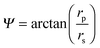 shows a decrease when the overlayer absorption increases.26 First, the spectra of Ψ during oxidation shall be discussed. With progressing oxidation, a bending in Ψ was observed at 380 nm, caused by the light absorption from the main electronic transition for the oxidic film (Fig. 3). During oxidation, this feature showed a much slower evolution with time than the layer thickness, as discussed in detail elsewhere.14 Previous analyses of the observed currents and the layer thicknesses have shown that metal dissolution occurs concurrently.14
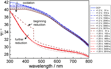 | ||
| Fig. 3 Spectra of ellipsometric Ψ for different times during anodic oxidation (+1.2 V) and subsequent cathodic reduction (−1.25 V). Arrows indicate the increasing time. | ||
Oxidation has been carried out at different electrode potentials. The spectra of Ψ obtained after 10 min oxidation are displayed in Fig. 4. The absorption feature at around 380 nm was visible for all potentials, though for treatment at high potentials the argumentation used for thin films is not valid any more, resulting in a maximum rather than a minimum in Ψ. Differences for layer thicknesses >10 nm are also confirmed by simulation of ellipsometric spectra using the optical constants as input parameters. The time evolution of the spectra and thickness of the layers at the different electrode potentials is shown in detail in the ESI.†
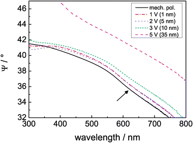 | ||
| Fig. 4 Comparison of Ψ after 10 min treatment at the indicated potential. In parentheses, the respective increase in thickness compared to the initial oxide thickness is given. For reference, the curve of a mechanically polished sample is also shown. The arrow points to the absorption feature at around 620 nm. | ||
A second interesting feature in the light absorption characteristics of the thin film was the minimum at around 620 nm (2 eV), which may be caused by intragap states.§ This feature becomes more obvious in plots of differences in and ratios in Ψ, which are presented in the ESI.† (The observation of photoluminescence, which will be discussed in Section 3.3, shows that this feature is not caused by elastic scattering of light, but rather light absorption.) This absorption in the visible spectral range is also crucial for the determination of the optical appearance: it determines the golden/brown colour shown in Fig. 1b. The absorption feature in Ψ was present in the samples treated between 1.2 V and 3.2 V, but absent in the sample treated at 5.2 V. During treatment at 5.2 V, the minimum gradually disappears (see ESI,† Fig. S12). This finding indicates that at low potentials, the oxide is richer in defects than at higher oxidation potentials, where films of larger thickness were obtained. These thicker films appeared white in colour. This result also implies that the defect-rich “native-like” oxide can be prepared up to thicknesses of ∼10 nm, while preparation is more difficult at higher thicknesses.
After oxidation, the samples were subjected to a reductive treatment at a potential of −1.25 V. At this potential, besides oxidereduction and redeposition of previously dissolved Zn, also H2 evolution occurs. As shown in Fig. 2c, upon the application of a cathodic potential the thickness of the oxide film changed to an apparent negative value (<−4 nm). This negative value to a large extent is related to the disappearance of the oxide layer present at OCP, though this was estimated to be 2–3 nm thick only.24,26 The overall ellipsometric data indicate a significant change in the interfacial layer upon the change in the electrode potential, faster than the experimental time resolution. A detailed observation of the current response (Fig. 2b inset) on the application of cathodic potential shows that there is a cathodic current peak for the reduction process. The negative current reached a maximum at ≈20 s after the application of the negative potential, and reached an almost stationary value within 60 s. Thus, there was an electrochemical reduction at the beginning, and the majority of this reduction process completed within 60 s. The measured Ψ (Fig. 3) shows a substantial change immediately after the potential jump to a cathodic potential.
From the electrochemical point of view, in agreement with previous ellipsometric analyses,14,32 the surface of the electrolyte should be oxide-free at the chosen reduction potential. The observed oxide on the surface should be formed during the process of removing the sample from the electrolyte and afterwards, i.e. should be a native oxide.
While the high wavelength region of the ellipsometric spectra was successfully analysed to yield a thickness, the overall curves after reduction for both Ψ and Δ were substantially different from the curves expected for a semi-infinite Zn half space without an overlayer, and different from curves observed at similar electrode potentials without prior oxidation.14 Deviations were found especially at lower wavelengths, as the light at lower wavelengths is scattered easier, which leads to the breakdown of the simple analysis of the full ellipsometric spectra based on a stratified system. These two observations indicate that the morphology of the surface changed after the electrochemical treatment. The effect of scattering on the polarisation of reflected light from a surface with a complex morphology also contributes to the obtained apparent values for the layer thickness difference after reduction.
3.3 Raman and photoluminescence spectroscopy
While analysis of ellipsometric spectra is affected by morphology changes, photoluminescence spectra show information about light absorption and subsequent emission independent of surface morphology. Here, the broad luminescence background in Raman spectra was analysed. Results are shown in Fig. 5. When excited at 325 nm, the oxidized sample showed a strong luminescence peak at ≈3.4 eV, typical for the main electronic transition of ZnO (Fig. 5a). In comparison, the luminescence of the electrochemically reduced sample is considerably lower. For the reduced sample, the thickness of the oxide had been reduced to its minimum. Therefore, no efficient absorption of light was possible in the chosen illumination geometry. A second possible explanation for the observed low luminescence intensity is the quenching effect by the continuum of states in the underlying metal. However, the situation was reversed when excited with 532 nm laser light. Here, the reduced sample showed a strong and broad background luminescence, indicating a strong luminescence, and the oxidized sample gave a much weaker luminescence. The maximum luminescence intensity in the reduced sample agrees approximately with the previously reported difference to the conduction band of 1.9 eV of an intragap state,24 and shows a decay to higher energies. This decay is caused by the tail states, which may span the complete gap for such a material. The observation of the PL at 532 nm implies the absorption of light at photon energies of 2.33 eV, due to the presence of intragap states in the reduced sample. These states lead to the absorption of light over a broad wavelength range, consequently to the dark colour of the sample. This finding is in agreement with previous results of the analysis of ellipsometric spectra of a native oxide on Zn.24 In the past, while green PL has been associated with O-deficiency orange emission has been associated with excess O (see e.g. the discussion in ref. 9). As the emission observed here is more on the lower energy side, it may be interpreted as being caused by excess oxygen atoms (e.g. interstitial oxygen).9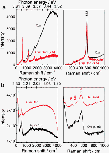 | ||
| Fig. 5 Raman spectra of electrochemically oxidized (“Oxi”, +1.2 V, 10 min) and subsequently reduced samples (“Oxi + Red”, −1.25 V, 1 min) excited with (a) 325 nm and (b) 532 nm. Both spectra at the respective wavelength were recorded under the same illumination conditions. Intensities for the sample “Oxi + Red” were multiplied by 5 in (a) while intensities for sample “Oxi” were multiplied by 10 in (b). The values on the photon energy scale correspond to the nearest second digit to the energy value of the respective Raman shift. The spectra on the left represent an overview spectrum while the spectra on the right show the region up to 1000 cm−1, the region of interest in the Raman spectra. | ||
The Raman spectra are also displayed in Fig. 5. The resonance Raman spectrum (excited at 325 nm, Fig. 5a) was dominated by a peak at 578 cm−1. In addition, as typical for resonance Raman spectra,33–35 the second order (≈1150 cm−1), third order (1725 cm−1), and for the reduced sample even the fourth (2300 cm−1) and fifth (2875 cm−1) order of the same mode were also observed. The Raman spectrum with excitation at 532 nm (Fig. 5b) showed a major peak at ≈555 cm−1, a shoulder at ≈440 cm−1 and a peak of low intensity at ≈370 cm−1. Intensities of the peaks were different between ‘oxidized’ and ‘oxidized + reduced’ samples, but the main peak positions remain the same. The dominating peak is attributed to the longitudinal optical (LO) phonon of ZnO.35–38 Other peaks are only observed when excited at 532 nm. The peak at ≈440 cm−1 is the characteristic E2 mode of the wurtzite lattice of ZnO, which dominates bulk spectra of crystalline ZnO.36,37 This mode was obvious for the oxidized sample but weak in the reduced sample. The situation was reversed for the mode at ≈380 cm−1, assigned to an A1 mode (TO phonon).35–37
There is general consensus in the literature that the dominance of the LO phonon in the Raman spectra is an indication of strong disorder in such systems.20,38–44 Dominance of these modes has been reported mainly for gas-phase deposited ZnO films,38,41,42 but also for films prepared by hydrothermal growth,43 or by electrochemical oxidation of Zn in KOH.20 Strong resonance enhancement of the features related to defects is not uncommon, and is consistent with the results found here.38,40
The strong shift of the LO phonon with excitation wavelengths is striking, especially the low wavenumber of the mode 555 cm−1 found when using 532 nm excitation. While the LO phonon mode is split into an A1 and an E1 mode, the difference in frequency between the two modes is reported as only 10 cm−1.36 Therefore, the splitting of the LO phonon alone and a domination of different components alone are likely not to be the reason for the observed difference. Different local bonding situation may contribute to the observed difference. Excitation of the main electronic transition by the 325 nm laser should yield resonance enhancement of all structural elements in the film. On the other hand, light at 532 nm was also absorbed, but as discussed above mainly by defect-induced electronic states. Differences in their local environment to the bulk material used in reference studies can contribute to the observed frequency shift. In addition, Raman enhancement with localized interface and/or surface phonon modes may contribute to the observed differences.33–35
Overall, the complete absence in the spectra at 325 nm, and the only weak contribution in the spectra at 532 nm, of the E2 mode at 440 cm−1 may be understood in a way that the native oxide formed during removal of the sample from the electrolyte is a highly disordered material, with only a minority of Zn atoms coordinated as in the wurtzite structure of crystalline ZnO.
3.4 Surface morphology and topography
The results of ellipsometric measurements after the reduction process have been found not to be well-described using the simple model of a homogeneous film on a flat surface. Therefore, the surface topography, roughness as well as morphology were examined by AFM and SEM. Fig. 6 shows AFM images of the sample surfaces after different treatments. A mechanically polished Zn surface (Fig. 6a) showed a root-mean-square (RMS) roughness of about 3 nm, and a peak-to-peak (PTP) roughness of ≈20 nm over an area of 10 μm. The roughness increased to 9 nm (RMS) and 40 nm (PTP) after electrochemical oxidation (Fig. 6b). The white protruding lines in Fig. 6b may be the grain boundaries, where the reactivity is higher. After subsequent electrochemical reduction, as shown in Fig. 6c, the surface became much rougher (RMS roughness 18 nm), and particles with a diameter of ≈170 nm and an average height of ≈60 nm were observed, which are distributed homogeneously on the surface. This result shows that the reduction step mainly serves as a nanostructuring step, which renders the ellipsometric analysis presented above insufficient to describe the complete spectrum.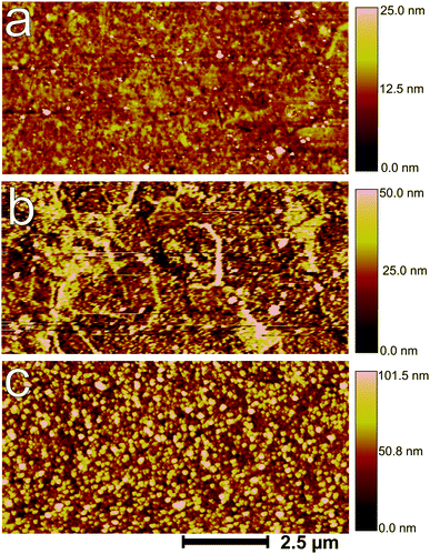 | ||
| Fig. 6 AFM images of (a) mechanically polished, (b) electrochemically oxidized (+1.2 V, 10 min) and (c) subsequently reduced (−1.25 V, 1 min) zinc. | ||
Fig. 7 shows the SEM images for the mechanically polished, electrochemically oxidized and subsequently reduced samples. Like the results from AFM, a featureless surface as shown in Fig. 7a indicates a mechanically well-polished surface. After electrochemical oxidation (Fig. 7b), the surface is still featureless. However, the morphology of the film changed significantly after short (1 min) electrochemical reduction. From Fig. 7c and d, one can see that hexagon shaped thin plates were homogeneously covering the sample surface. The plates had an average diameter of 70–100 nm and an estimated thickness of 20–30 nm.
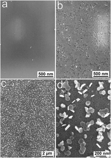 | ||
| Fig. 7 SEM images of (a) mechanically polished, (b) electrochemically oxidized (+1.2 V, 10 min) and (c and d) subsequently reduced (−1.25 V, 1 min) samples. | ||
Density and size of the nanoplates are influenced by the reduction time, as well as the duration of prior oxidation. Fig. 8 shows a series of SEM images for a sample oxidized at +1.2 V for 10 min, which was subsequently reduced at −1.25 V for different times. When the reduction time was only 10 s as shown in Fig. 8a, the coverage of the surface with nanoplates was not homogeneous. A closer look (Fig. 8b) indicates that the nanoplates are present only in certain places, which one may speculate could be linked to grain boundaries. The overall coverage is about 20% of the surface area. The coverage increases with reduction time, and more than 50% of the surface is covered with nanoplates after 30 s reduction (Fig. 8c and d). After 1 min reduction, the surface is covered homogeneously with the nanoplates, as shown in 7c and d. The maximum amount of the nanoplates is obtained after 2 min reduction (Fig. 8e and f). Coverage does not change with longer reduction time. For reduction times >10 s, some neighbouring plates appear to join. With increasing reduction time, the size of the nanoplates also increases. The diameter changes from 15–20 nm (reduction for 10 s) to 90–110 nm (reduction for 60 s and longer).
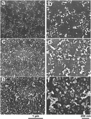 | ||
| Fig. 8 SEM images of a Zn sample after the electrochemical oxidation at +1.2 V for 10 min and subsequent reduction for different times, (a and b) 10 s, (c and d) 30 s, and (e and f) 120 s at −1.25 V. The 1 μm scale bar under (e) applies to all images in the left column (a, c, and e), while the 200 nm scale bar under (f) applies to all images in the right column (b, d, and f). | ||
The control experiment mentioned in Section 3.1, in which an electrolyte is used that does not contain Zn2+ also showed the presence of nanoplates after the reduction step. Therefore, the occurrence of the nanoplates must be linked to the reduction of the oxide layer. From the SEM images of the surface after reduction, for the sample reduced only for 10 s, the nanoplates formed partially inside the film (see Fig. 8b and d). Therefore, reduction of the thick oxide film results in the occurrence of the nanoplates in the regions from where the film was removed.
The oxidation potential prior to reduction also has an effect on the resulting nanoplates. At lower oxidation potentials, e.g. +1.2 V, at least 5 min are needed before nanoplates were detected. Less time is needed for nanoplate formation at higher oxidation potentials, e.g. ca. 30 s suffice at +5.2 V. This potential dependence may indicate that a certain amount of oxide is needed to produce nanoplates upon reduction.
3.5 Surface analysis
A chemical analysis of extended ranges of the surface after different electrochemical treatment was carried out by XPS. Depth profiles of the sample were obtained by combining a sequence of Ar ion gun etch cycles interleaved with XPS measurements from the freshly exposed surface. High resolution XPS were acquired at every interval after etching. Fig. 9 shows the sputtering profiles obtained by XPS of differently treated samples. All experimental data have been fit using the minimum number of peaks to obtain an appropriate fit. Characterisation of mechanically polished samples has been reported previously.24,26 For these samples an oxide layer thickness was estimated to be 2–4 nm.24,26 As shown in Fig. 9a and c, compared with the electrochemically oxidized sample, the intensity of the O1s peak differed substantially after electrochemical reduction, even when the reduction lasts only for 60 s. The O1s peak disappeared after little more than 7 nm for the oxidized sample, but this peak could not be observed after 2–3 nm sputtering for the reduced sample. A similar trend was observed from the Auger process during the XPS in the Zn LMM peaks at the different sputter depths, as shown in Fig. 9b and d. Moreover, compared with the parameter-free ellipsometric analysis14 performed for the oxidized sample the thickness obtained here on the basis of SiO2 is in good agreement, because of the similarities in the sputter rates for ZnO and SiO2.29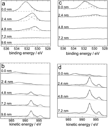 | ||
| Fig. 9 XPS sputter profiles of the O1s region (a and c) and Zn LMM Auger peaks during XPS (b and d) of electrochemically oxidized (+1.2 V, 10 min) samples (a and b) and subsequently reduced (−1.25 V, 1 min) samples (c and d). | ||
The O1s peak (Fig. 9a and c) consists of at least 2 components, centred at binding energies of ∼532 eV and ∼530.5 eV, respectively. The component at 532 eV has previously been assigned to hydroxidic oxygen, while the other component was assigned to oxidic oxygen.26,28 At higher sputtering depths, the oxidic component dominates. The component at 532 eV may contain contributions from carbonate oxygen as well. Similar to previous results,26 evidence for the presence of carbonate in small amounts was found from the C1s peaks only directly at the surface. Already after the first sputtering step, no carbonate was found any more. The Zn LMM Auger peaks, shown in Fig. 9b and d, show the transformation from predominantly ZnII at the surface to metallic Zn0 in the bulk material.24 While the depth of the transition from metals to oxides was different comparing oxidized and subsequently reduced samples, the observed behaviour was qualitatively the same for both kind of samples. Hence, no difference was observed for the chemical species found at the surface of the two differently treated surfaces. It must be stressed again that in the case of the reduced samples, the oxide forms during removal of the sample from the electrolyte.
The formation of hexagon shaped nanoplates as observed after the reduction is a hint for the formation of a crystalline material, typically crystals on the nanometre scale. XRD was used to obtain crystallographic information. Fig. 10 shows the XRD patterns of the mechanically polished, oxidized and subsequently reduced Zn samples. Due to the low thickness of the oxide layer during the oxide process (2–3 nm for native oxide film on the mechanically polished sample, ∼10 nm for the electrochemically oxidized sample), peaks representing metallic zinc dominate the patterns. The strongest peak for polycrystalline zinc is the Zn{101} peak located at a scattering angle 2θ = 43.2° (PDF no. 03-065-3358), so all the peaks were normalized to this peak for a better comparison. It must be pointed out that the Zn{002} peak at 2θ = 36.29° is very close to the ZnO{101} peak at 2θ = 36.25°, the strongest peak for ZnO (PDF no. 00-005-0664), and it is not possible to distinguish them at the resolution used here. After electrochemical oxidation, the relative intensity of the peaks at 2θ = 36.3° and 2θ = 43.2° changed significantly. For a mechanically polished sample, the intensity ratio between these two peaks is ≈1.9, close to that of polycrystalline zinc (PDF no. 03-065-3358). The ratio changes to ≈0.4 after electrochemical oxidation. In the logarithmic plot in Fig. 10b, in addition to the main peaks as in Fig. 10a, two broad weak peaks at 31.8° and 56.5° appeared, representing ZnO{100} and {110}, respectively. The large width of these peaks shows that the oxide, which was formed on Zn, is either amorphous or relatively small crystal size. Assuming nanocrystalline material, an estimate based on the Debye–Scherrer formula indicates the newly formed oxide after oxidation has a diameter of less than 10 nm. It must be pointed out that crystalline domains in thin films like studied here are expected to show rather strong differences in size parallel to the interface compared to the direction perpendicular to the interface.
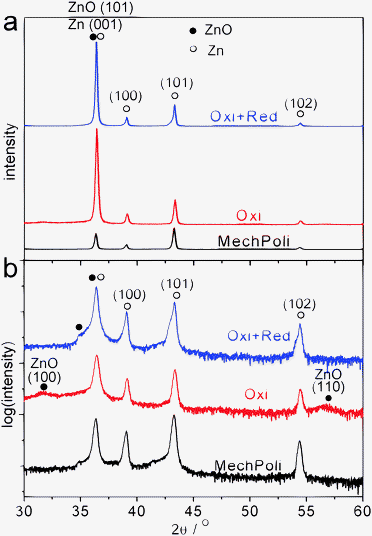 | ||
| Fig. 10 Linear (a) and logarithmic (b) plots of XRD of mechanically polished (“MechPoli”), electrochemically oxidized (“Oxi”, +1.2 V, 10 min) and subsequently reduced samples (“Oxi + Red”, +1.2 V, 10 min and −1.25 V, 1 min). ˙ indicates peaks for ZnO and ○ indicates peaks for Zn. Curves have been offset for clarity. | ||
The change in the intensity ratio between the peaks at 2θ = 36.3° and 2θ = 43.2° cannot be explained by an increase in diffraction from a macroscopically crystalline ZnO phase. Instead, the relative decrease in intensity of the peak at higher 2θ is attributed to the generation of defects in the near-surface region of the metallic bulk during the electrochemical treatment, and consequent loss in order affecting diffraction at higher 2θ with an increase in peak width to a larger extent. If the oxidized sample was subsequently electrochemically reduced (1 min), the intensity ratio of the two peaks changes to ≈0.7. To compare the peaks more clearly, the logarithm of the intensity was plotted, as shown in Fig. 10b.
The question of the composition of the nanoplates observed using SEM and AFM has still to be answered. This question has been addressed using AES on the plates and in regions where no plate was present. Fig. 11 shows the AES of the sample surface on and off the nanoplate. In addition, two reference spectra from the instrument's database are presented for comparison. The spectrum recorded on the plate closely resembles the spectrum of oxide-free metallic Zn, as opposed to the spectrum in the region where no plate was present. Quantitative analysis on the basis of the algorithms implemented in the instrument's software shows that on the nanoplate's surface without any sputtering, the atomic concentration of metallic Zn is 33%, about two times as high compared with the area of nanoplates, where a concentration of 17% is found. This result shows the nanoplates to consist of Zn, rather than of ZnO. It needs to be stressed again that the oxide observed on the reduced sample is in large portions formed during removal of the sample from the electrolyte. AES does, however, show that the plates are not residual oxidese.g. present from before the reduction process.
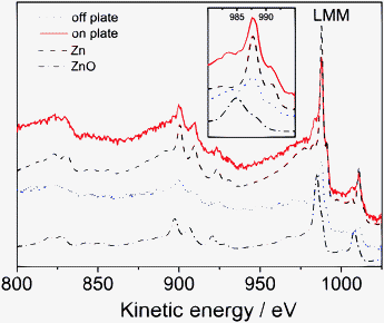 | ||
| Fig. 11 AES of the “Oxi + Red” sample on the region with nanoplates and without plate, compared to reference spectra of pure ZnO and pure Zn. The inset shows a magnification of the LMM region. | ||
4 Summary and conclusions
The electrochemical oxidation of Zn produces an oxide with intragap states. The intragap states observed increase the absorption of light in the visible spectral range. SE and PL measurements show the existence of a donor level of ≈1.8 eV below the bottom of the conduction band, at a total band gap of 3.4 eV for ZnO. A schematic view of the band structure is shown in Fig. 12a. The absorption of light in this oxide makes the surface appear dark grey. The oxide itself – typical for many ill-defined oxides of this type – is an extreme case in the density of defects. PL spectra point to a dominance of excess oxygen atoms as main sources of the defects. The Raman spectra may be interpreted in a way that full wurtzite-type elementary cells are almost absent in the oxide obtained. Higher oxide thicknesses, which are obtained at higher oxidation potentials, lead to oxidic films which become more bulk-like.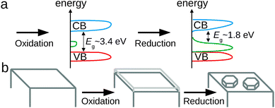 | ||
| Fig. 12 (a) Schematic view of the oxide band structure before and after electrochemical reduction with subsequent removal from the electrolyte. (b) Schematic view of the formation of the final morphology in the process of different electrochemical treatments. | ||
The actual nature of the states in the band gap is not directly clear from the experimental evidence presented in this work. The most likely sources are defects inside the thin oxide film. The presence of surface defects, producing surface states, is also consistent with the observed Raman and PL spectra. The presence of e.g. an –OH (or other) termination on the surface cannot be excluded. There are, however, no direct hints on an effect of this surface termination on the resulting electronic structure.
The reduction of a previously produced oxide furthermore leads, in a solid-state reaction, to the formation of plate-like Zn nanostructures, as shown schematically in Fig. 12b. In particular, redeposition of Zn can be ruled out as a Zn source of the nanostructures. Formation of these structures can be explained by the reduction in volume when reducing amorphous oxides to crystalline Zn. The structures have typically a diameter of 70–100 nm and a height of 30–100 nm. After reduction, the golden/brown colour of the material, SE and PL results indicate that the electronic structure of the oxide formed after removal of Zn from solution (and the consequent reoxidation of the surface through water and oxygen) is dominated by defect states: the main electronic transition of bulk ZnO is not observed in this material any more, making it an extreme case of a defect-dominated material. In this material, the band gap has effectively been reduced to 1.8 eV. It must be pointed out that the stepwise reduction performed here is responsible for the extreme properties of the obtained oxides. If an electrochemical reduction is performed with a gradual decrease in electrode potential, no nanostructured surfaces are obtained.14 After reduction, the black colour of the material, in addition to ellipsometric spectra as well as the PL results, indicates that the electronic structure of the oxide formed after removal of Zn from solution is dominated by defect states. The main electronic transition of bulk ZnO is not observed in this material any more, making it an extreme case of a defect-dominated material. In this particular example, both surface morphology as well as electronic structure of the oxide on the surface are affected by the electrochemical process. The conclusion from the work here is that the dark appearance especially of the reduced samples is a result of a synergistic effect of morphology and oxide electronic structure. Interesting electronic and photonic properties of ZnO have previously been related to defects in the material.38 As the states produced by “electrochemical electronic structuring” can be populated for a sufficient time to show PL, the materials produced here may also be useful as photocatalysts.
Acknowledgements
Y. C. thanks for support from the European Union and the state of North Rhine-Westphalia in the frame of the HighTech.NRW program. P. S. acknowledges support from Salzgitter Mannesmann Forschung GmbH in the frame of the International Max Planck Research School for Surface and Interface Engineering in Advanced Materials (IMPRS-SurMat). Prof. Stratmann is acknowledged for his continuous support. The MPIE machine shop is acknowledged for the building of the in situ SE cell.References
- A. Janotti and C. G. Van de Walle, Rep. Prog. Phys., 2009, 72, 126501 CrossRef.
- A. B. Djurisic, X. Chen, Y. H. Leung and A. Man Ching Ng, J. Mater. Chem., 2012, 22, 6526–6535 RSC.
- S. Lany and A. Zunger, Phys. Rev. B: Condens. Matter Mater. Phys., 2005, 72, 035215 CrossRef.
- H. von Wenckstern, H. Schmidt, M. Brandt, A. Lajn, R. Pickenhain, M. Lorenz, M. Grundmann, D. Hofmann, A. Polity, B. Meyer, H. Saal, M. Binnewies, A. Borger, K.-D. Becker, V. Tikhomirov and K. Jug, Prog. Solid State Chem., 2009, 37, 153–172 CrossRef CAS.
- H. Zeng, G. Duan, Y. Li, S. Yang, X. Xu and W. Cai, Adv. Funct. Mater., 2010, 20, 561–572 CrossRef CAS.
- W. Chen, Y. Qiu and S. Yang, Phys. Chem. Chem. Phys., 2012, 14, 10872–10881 RSC.
- Y. Zhang, M. K. Ram, E. K. Stefanakos and D. Y. Goswami, J. Nanomater., 2012, 2012, 624520 Search PubMed.
- H. J. Lewerenz, C. Heine, K. Skorupska, N. Szabo, T. Hannappel, T. Vo-Dinh, S. A. Campbell, H. W. Klemm and A. G. Munoz, Energy Environ. Sci., 2010, 3, 748–760 CAS.
- J. Wang, P. Liu, X. Fu, Z. Li, W. Han and X. Wang, Langmuir, 2009, 25, 1218–1223 CrossRef CAS.
- J. Wang, Z. Wang, B. Huang, Y. Ma, Y. Liu, X. Qin, X. Zhang and Y. Dai, ACS Appl. Mater. Interfaces, 2012, 4, 4024–4030 CAS.
- X. Zhang, Corrosion and Electrochemistry of Zinc, Plenum Press, New York, 1996 Search PubMed.
- C. Leygraf and T. Graedel, Atmospheric Corrosion, Wiley-Interscience, New York, 1st edn, 2000 Search PubMed.
- M. Mokaddem, P. Volovitch and K. Ogle, Electrochim. Acta, 2010, 55, 7867–7875 CrossRef CAS.
- Y. Chen and A. Erbe, Surf. Sci., 2013, 607, 39–46 CrossRef CAS.
- J. Buchholz, Surf. Sci., 1980, 101, 146–154 CrossRef CAS.
- P. Hayfield, Surf. Sci., 1976, 56, 488–507 CrossRef CAS.
- L. M. Baugh, Electrochim. Acta, 1979, 24, 657–667 CrossRef CAS.
- D. C. W. Kannangara and B. E. Conway, J. Electrochem. Soc., 1987, 134, 894–906 CrossRef CAS.
- B. E. Conway and D. C. W. Kannangara, J. Electrochem. Soc., 1987, 134, 906–918 CrossRef CAS.
- W.-B. Cai and D. A. Scherson, J. Electrochem. Soc., 2003, 150, B217–B223 CrossRef CAS.
- S. Bonk, M. Wicinski, A. W. Hassel and M. Stratmann, Electrochem. Commun., 2004, 6, 800–804 CrossRef CAS.
- X.-L. Shang, B. Zhang, E.-H. Han and W. Ke, Electrochim. Acta, 2011, 56, 1417–1425 CrossRef CAS.
- J. W. Schultze and A. W. Hassel, Passivity of Metals, Alloys and Semiconductors, in Encyclopedia of Electrochemistry, ed. A. Bard, M. Stratmann and G. Frankel, Wiley-VCH, Weinheim, 2007, vol. 4, pp. 216–235 Search PubMed.
- J. Zuo and A. Erbe, Phys. Chem. Chem. Phys., 2010, 12, 11467–11476 RSC.
- Z. Mekhalif, L. Massi, F. Guittard, S. Geribaldi and J. Delhalle, Thin Solid Films, 2002, 405, 186–193 CrossRef CAS.
- Y. Chen, P. Schneider and A. Erbe, Phys. Status Solidi A, 2012, 209, 846–853 CrossRef CAS.
- J. Lekner, Theory of Reflection of Electromagnetic and Particle Waves, M. Nijhoff, Dordrecht, 1987 Search PubMed.
- R. Benoit, Y. Durand, B. Narjoux and G. Quintana, http://www.lasurface.com/, 2012.
- D. R. Baer, M. H. Engelhard, A. S. Lea, P. Nachimuthu, T. C. Droubay, J. Kim, B. Lee, C. Mathews, R. L. Opila, L. V. Saraf, W. F. Stickle, R. M. Wallace and B. S. Wright, J. Vac. Sci. Technol., A, 2010, 28, 1060–1072 CAS.
- V. Tolstoy, I. Chernyshova and V. Skryshevsky, Handbook of infrared spectroscopy of ultrathin films, Wiley, Hoboken, New Jersey, USA, 2003 Search PubMed.
- M. Debe, Prog. Surf. Sci., 1987, 24, 1–282 CrossRef CAS.
- A. Hamnett and R. J. Mortimer, J. Electroanal. Chem., 1987, 234, 185–192 CrossRef CAS.
- J. F. Scott, Phys. Rev. B: Condens. Matter Mater. Phys., 1970, 2, 1209–1211 CrossRef.
- X. T. Zhang, Y. C. Liu, Z. Z. Zhi, J. Y. Zhang, Y. M. Lu, D. Z. Shen, W. Xu, G. Z. Zhong, X. W. Fan and X. G. Kong, J. Phys. D: Appl. Phys., 2001, 34, 3430–3433 CrossRef CAS.
- C. Roy, S. Byrne, E. McGlynn, J.-P. Mosnier, E. de Posada, D. O'Mahony, J. G. Lunney, M. O. Henry, B. Byan and A. A. Cafolla, Thin Solid Films, 2003, 436, 273–276 CrossRef CAS.
- T. C. Damen, S. P. S. Porto and B. Tell, Phys. Rev., 1966, 142, 570–574 CrossRef CAS.
- C. A. Arguello, D. L. Rousseau and S. P. S. Porto, Phys. Rev., 1969, 181, 1351–1363 CrossRef CAS.
- Y. Y. Tay, T. T. Tan, M. H. Liang, F. Boey and S. Li, Appl. Phys. Lett., 2008, 93, 111903 CrossRef.
- S. Permogorov and A. Reznitsky, Solid State Commun., 1976, 18, 781–784 CrossRef CAS.
- P. Lottici and C. Razzetti, Solid State Commun., 1978, 25, 427–430 CrossRef CAS.
- G. J. Exarhos and S. K. Sharma, Thin Solid Films, 1995, 270, 27–32 CrossRef CAS.
- K. Saw, K. Ibrahim, Y. Lim and M. Chai, Thin Solid Films, 2007, 515, 2879–2884 CrossRef CAS.
- M. Guo, P. Diao and S. Cai, Appl. Surf. Sci., 2005, 249, 71–75 CrossRef CAS.
- H. Liu, G. Piret, B. Sieber, J. Laureyns, P. Roussel, W. Xu, R. Boukherroub and S. Szunerits, Electrochem. Commun., 2009, 11, 945–949 CrossRef CAS.
Footnotes |
| † Electronic supplementary information (ESI) available: Time evolution of oxide thickness and ellipsometric spectra during electrochemical treatment at different electrode potentials. See DOI: 10.1039/c3cp44714f |
| ‡ Present address: Department of Electrochemistry and Conducting Polymers, Leibniz-Institut für Festkörper- und Werkstoffforschung Dresden, Helmholtzstrasse 20, 01069 Dresden, Germany. |
| § By “intragap states”, the authors refer to an energetic state within the bandgap. Surface states with an appropriate energy fall into this group, as defect states in the thin film of appropriate energy. |
| This journal is © the Owner Societies 2013 |