Creating, characterizing, and controlling chemistry with SERS hot spots
Samuel L.
Kleinman
,
Renee R.
Frontiera
,
Anne-Isabelle
Henry
,
Jon A.
Dieringer
and
Richard P.
Van Duyne
*
Northwestern University, Department of Chemistry, 2145 Sheridan Rd., Evanston, IL 60208, USA. E-mail: vanduyne@northwestern.edu
First published on 17th September 2012
Abstract
In this perspective we discuss the roles of hot spots in surface-enhanced Raman spectroscopy (SERS). After giving background and defining the hot spot, we evaluate a variety of SERS substrates which often contain hot spots. We compare and discuss the differentiating properties of each substrate. We then provide a thorough analysis of the hot spot contribution to the observed SERS signal both in ensemble-averaged and single-molecule conditions. We also enumerate rules for determining the SERS enhancement factor (EF) to clarify the use of this common metric. Finally, we present a forward-looking overview of applications and uses of hot spots for controlling chemistry on the nanoscale. Although not exhaustive, this perspective is a review of some of the most interesting and promising methodologies for creating, controlling, and using hot spots for electromagnetic amplification.
 Samuel L. Kleinman | Samuel Louis Kleinman received a BS in chemistry from the University of California, Berkeley. He received a PhD in physical chemistry from the laboratory of Richard P. Van Duyne at Northwestern University. His thesis research focused on structure–function relationships in single-molecule and single-nanoaggregate surface-enhanced Raman spectroscopy. He currently continues this research as a post-doctoral fellow at Northwestern University. His interests include lithographic techniques for generating new and exciting plasmonic nanostructures for ultrasensitive detection platforms. |
 Renee R. Frontiera | Renee R. Frontiera received her BA in Chemistry and Chinese linguistics from Carleton College in 2004. She carried out her PhD work with Professor Richard A. Mathies at the University of California—Berkeley, on the use of femtosecond stimulated Raman spectroscopy to examine ultrafast vibrational dynamics and anharmonic couplings. She is currently a postdoctoral researcher with Professor Richard P. Van Duyne at Northwestern University, developing new ultrafast plasmonic spectroscopies in order to monitor plasmonically enhanced reactions and to examine molecule–plasmon coupling effects. |
 Anne-Isabelle Henry | Anne-Isabelle Henry received a BS in physical chemistry from University Paris Sud (2003) in Orsay, France after completing an internship in the Department of Physical Chemistry at the Fritz Haber institute in Berlin, Germany. She received a PhD (2008) in chemistry from University Pierre and Marie Curie in Paris, France on the thermal stability and control of superstructure in Ag nanocrystals assemblies. She is currently a senior research associate at Northwestern University. Her research interests include the fabrication, assembly, and study of plasmonic nanoparticles, SERS-active nanoparticle aggregates and substrates with a focus on structure–property relationships. |
 Richard P. Van Duyne | Richard P. Van Duyne is Charles E. and Emma H. Morrison Professor of Chemistry and of Biomedical Engineering at Northwestern University. He received a BS (1967) at the Rensselaer Polytechnic Institute and PhD (1971) at the University of North Carolina, Chapel Hill, both in chemistry. He is a member of the National Academy of Sciences and the American Academy of Arts and Sciences. He is known for the discovery of surface-enhanced Raman spectroscopy (SERS), the invention of nanosphere lithography (NSL), and development of ultrasensitive nanosensors based on localized surface plasmon resonance (LSPR) spectroscopy. |
I. Introduction
Surface-enhanced Raman spectroscopy (SERS) was first discovered in 1977 when optical spectroscopists did not commonly practice surface analysis and nanoscale imaging techniques.1 Approximately ten years after the discovery of SERS, the use of high-resolution transmission electron microscopy (HRTEM) experiments enabled nanometer scale images of SERS active substrates, thus defining a SERS “hot spot”.2,3 However, early practitioners of SERS had to rely on other methods to determine the potential sources of enhancement.Early work suggested an electromagnetic enhancement mechanism for SERS which involves the localization and amplification of incident light fields by a surface plasmon resonance.1 This mechanism mediates the sensitive detection of molecular vibrations at noble metal surfaces. In concert with a chemical enhancement mechanism and other surface effects, typical SERS enhancement factors (EF—the increase in signal per molecule) are order 103–7. Certain high performance SERS substrates have achieved average EFs >108. The analytical applications for these surfaces have been exploited for ultrasensitive detection and sensing of biological systems, chemical warfare agents, and small molecules, amongst others.4–6 Strongly enhancing SERS substrates can provide molecular identification but also enable single-molecule vibrational spectroscopy7 and can be used as light-gathering antennas which can mediate photochemical processes.8,9
In 1997, two nearly simultaneous reports were published claiming single-molecule detection and SERS became the first vibrational spectroscopy to achieve the ultimate limit of detection for chemical systems.7,10 Regions of very high electromagnetic enhancement are necessary to observe the Raman scattering of a single molecule. The seminal discovery of single-molecule SERS (SMSERS) by the groups of Nie7 and Kneipp10 was then followed by the work of Brus and coworkers11 who used scanning probe microscopy (SPM) to image the structural features at the origin of this phenomenon. This provided the first evidence that SMSERS originated from nanoparticle aggregates. Aggregates necessarily contain a nanoparticle junction—the hypothesized and theoretically confirmed hot spot location.12 In light of the recent discussion as well as that contained herein we define a ‘hot spot’. That is, a junction or close interaction of two or more plasmonic objects where at least one object has a small radius of curvature on the nm scale. This structural motif has the ability to concentrate an incident electromagnetic field and effectively amplify the near field between and around the nanostructures. This functional definition will be used within this manuscript; however, it should be noted that others may expand the definition of a hot spot to regions of high curvature on individual plasmonic particles.13
Motivated by the need to quantify the electromagnetic enhancement within a hot spot-containing structure, computational studies using the finite element method (FEM), the finite-difference time-domain (FDTD) method, discrete dipole approximation (DDA), and the generalized multipole Mie (GMM) analysis have appeared as an ideal complement to experimental studies,14–16 such as correlated localized surface plasmon resonance (LSPR)-TEM-SERS experiments at the single aggregate/nanoparticle level.17 Early work on electromagnetic modelling of dimers was conducted by Rojas and Claro,18 and expanded upon by Käll and co-workers.19 This fundamental work has given modern day researchers a vast array of tools and theories to analyze complex computational problems. As such, computational methods are a valuable tool to simulate the electric field intensities in the vicinity of hot spots, and thus help quantify the intensities and dimensions of hot spots. Furthermore, computational studies have guided the design of highly enhancing motifs for achieving maximum enhancements.15,20,21Fig. 1 shows computed field intensities around a dimer of nanospheres; the hot spot is depicted as the yellow region located between the circles in this cross-sectional view.
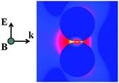 | ||
| Fig. 1 Local FDTD calculation showing |E|2/|E0|2 contour profiles for a gold dimer (100 nm cylinders) with a 0.5 nm gap. Regions of largest enhancement are yellow, moderate enhancement is red and little to no enhancement is blue. Adapted with permission from ref. 16. | ||
This perspective will discuss the role of hot spots in SERS and beyond. First, various methods for the formation of hot spots will be discussed, including top-down and bottom-up fabrication methods, chemical synthesis, and self-assembly of nanoantennas. In the next section, the benefits and consequences of hot spots will be discussed, specifically their effect on measurement of the EF. Finally, multiple applications of SERS hot spots will be highlighted, including: ultrahigh resolution lithography, non-linear spectroscopy, photocatalysis and photovoltaics.
II. Generation of hot spots
The design of substrates maximizing the electromagnetic enhancement has been a major research interest over the last ten years or so, made possible by the development of nanofabrication methods and motivated by the need for controlled, robust, and reliable SERS-active substrates. It is now apparent that the presence of hot spots on SERS substrates is responsible for a large part of the average enhancement. That is, SERS substrates with no hot spots such as a silver island film (AgIF) serve to enhance the total signal by about 103 yet SERS substrates which incorporate hot spots can raise the average enhancement well above 106.4 Both top-down and bottom-up nanofabrication strategies are being explored for the generation of hot spots. Through the description of some promising methods developed within those two approaches, we will discuss in this section the advantages and challenges remaining for achieving highly-sensitive, hot spot-laden, and reproducible substrates over macroscopic areas. We have constructed Table 1 for a quick comparison of the attributes of the SERS substrates discussed subsequently.| EF range | Estimated gap size (nm) | Cost ($-$$$$) | Analyte specificity | Proven SM sensitivity | Ref. | |
|---|---|---|---|---|---|---|
| Non-hot spot substrates | ||||||
| Island films | 104 | 10–100 | $$ | No | Yes | 22–24 |
| Periodic particle array | 107 | 10–100 | $$ | No | No | 4, 25 |
| Nanorods | 103–107 | NA | $ | No | No | 26 |
| Nanoshells | ∼106 | NA | $ | No | No | 27 |
| Fabricated substrates | ||||||
| MFONs | 103–1011 | 0.1–10 | $$ | No | No | 28, 29 |
| Lace-shell NPs | ∼102 | 1–10 | $$ | No | No | 30 |
| Fs laser etching | <109 | NR | $$$ | No | No | 31, 32 |
| E-beam lithography | 103–105 | 1–100 | $$$$ | No | No | 33–35 |
| Templated nanowires | 102–103 | 5–100 | $$ | No | No | 36–38 |
| Bowtie electromigration | 108 | 0.1–10 | $$ | No | No | 39 |
| Spheres on E-beam posts | 108 | 0–1 | $$$$ | Yes | No | 40 |
| Assembled structures | ||||||
| Aggregated colloids | 106–1010 | 0–10 | $ | No | Yes | 7, 41 |
| DNA hybridization | 108–1012 | 1–100 | $$ | Yes | Yes | 42–44 |
| Embedded polymers | ∼105 | 10–100 | $ | No | No | 45, 46 |
| SiO2 encapsulated cores | 106–108 | 0–10 | $$ | Yes | No | 47 |
| Particles in wells | 109 | 0–10 | $ | No | No | 48, 49 |
| Nanofingers | 1010–1011 | 0–10 | $$$$ | No | No | 50, 51 |
| TERS | 104–109 | 0–100 | $$$ | No | Yes | 52–54 |
| SHINERS | 105–108 | 1–10 | $ | No | No | 55, 56 |
II.A. Fabrication-generated hot spots
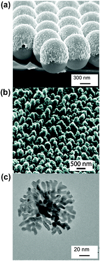 | ||
| Fig. 2 Hot spots fabricated without precise control of location and geometry. (a) SEM image of an Ag film over nanospheres (FONs) made by thermal deposition. (b) Helium ion microscope image (45°) of an Ag SERS substrate nanostructured by the ‘hot spot isolation’ process. (c) TEM of Au lace shell nanoparticle with built-in hot spots. Parts b and c reproduced with permission from ref. 32 and 30, respectively. | ||
Recently, Diebold et al. reported a method intending to isolate the hot spots on a nanostructured surface.32 In this study, a nanostructured Ag-covered silicon surface31 is covered by a photoresist and submitted to a femtosecond pulsed laser beam. The selective exposure of some areas is intensity-dependent. The authors conclude that only the hot spots are developed, based on the assumption that the multiphoton-induced luminescence is greatest in the hot spot. The resulting substrate is shown in Fig. 2b. The high-density of nanostructured features all have relatively high EFs. This substrate is especially attractive for limited analyte quantities.
Bottom-up fabrication of hot spot containing nanostructures includes the synthesis of nanoparticles with built-in hot spots, resulting from crevices between branches or protrusions on the particle surface. Examples of built-in hot spots nanoparticles include lace-shell nanoparticles, shown in Fig. 2c,57 or branch-like protrusions on single metallic nanoparticles.58–60 Although these are versatile structures with relatively facile synthesis, their enhancing capabilities and long-term stability can be somewhat limiting.
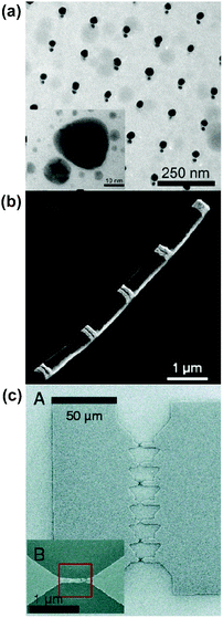 | ||
| Fig. 3 In situ controlled fabrication of hot spots with nm-scale gaps (a) TEM image (and high-magnification in inset) of Ag nanoparticle pairs fabricated by electron beam lithography combined with an angle evaporation technique. (b) Field-emission SEM image of a wire made of Au disks (white stripes on the image) fabricated by on-wire lithography (OWL). (c) SEM image of lithographically fabricated bowtie array made by electromigration (between extended electrodes). Parts a, b, and c reproduced with permission from ref. 61, 38 and 39, respectively. | ||
Another technique to obtain fine control of interparticle distance is to combine lithographic techniques with sacrificial templates. In particular, the use of matrices such as porous anodic aluminium oxide (AAO) templates has been reported by different groups to grow metallic nanowires of controlled diameter by electrochemical deposition.36–38 The ready availability and low cost of AAO production materials makes this method of fabricating hot spots feasible for massively parallel production of sensing substrates.
Moskovits and co-workers used templates to control the distance between the metallic wires down to ∼20 nm.36 Mirkin and co-workers achieved selective etching of parts of a bimetallic wire by a wet chemical process allowing the precise control of gaps as small as 5 nm. The selective etching is made possible by growing Au–Ag or Au–Ni in layers within the wire so that the etching of the interstitial layer would leave an empty space—the hot spot. A striking result from this study by Qin et al. is that the highest enhancement measured for pairs of 120 nm-thick Au disks with a ∼30 nm gap distance is not the smallest one (5 nm in this experiment). This observation was semi-quantitatively confirmed by local electric field calculations using the DDA. A sample image of this substrate is given in Fig. 3b. It was argued that the decline in field enhancement for very small gaps was the result of the redshift induced on the plasmon resonance, thereby moving it away from the laser excitation and Raman-scattered photon frequencies.38 This study is an example of how highly tailorable substrate creation allows examination of fundamental physics.
Lithography can also be combined with electrochemical methods for the fine-tuning of gap dimensions. Starting from an array of bowtie structures terminated by constrictions (∼80–100 nm wide), Halas and co-workers have applied electromigration at their tips to rearrange atomic positions, forming fine nanobridges. The resulting atomic migration-created gaps have widths ranging from <1 nm to a few nm, depicted in Fig. 3c.39 Resulting SERS spectra taken with the nanogap substrate showed high enhancements along with blinking and spectral diffusion, indicative of sensitivity approaching the single molecule level. This method of electromigration on lithographically-formed features offers the advantage of relatively high-yield and reproducible fabrication of SERS hot spots, with EFs easily reaching the 108 range.
Associating top-down, e.g. EBL, and bottom-up methods is an interesting way to achieve precise, parallel hot spot fabrication over surfaces. Gopinath et al. demonstrated this combined technique by directly synthesizing Au spheres onto aperiodic patterns of EBL-fabricated Au posts 200 nm in diameter. Once decorated with the small nanospheres, the long-range diffractive coupling resulting from the underlying post structure adds to the short-range electromagnetic response of the dimer particle-post construct.40 This combined method allows the creation of SERS-active hot spots to be further augmented by the underlying substrate, which also has an interaction with the exciting field. Combining random adsorption of nanoparticles with periodic surfaces has the benefit of ‘double-dipping’ on electromagnetic interactions. This idea could be expanded to other periodic SERS substrates as well.
In summary, lithography, especially with other techniques, has proven to be a valuable tool for the fabrication of controlled-size gaps down to ∼1–2 nm—the size range where maximum electromagnetic enhancement is expected. Different variants of lithography allow the researcher to choose the method most appropriate for the experiment at hand, whether it is fundamental single hot spot spectroscopy or the creation of large-scale sensing substrates.
II.B. Assembly-generated hot spots
The assembly of colloids is a very efficient way to obtain electromagnetic hot spots as the distance between the two metallic particles can be tuned down to one nanometre or less. To this end, different strategies have been developed for inducing aggregation of the plasmonic particles through chemical or mechanical processes. Strategies range from simple modulation of the electrostatic interactions between colloids—used in the first SMSERS reports7,10—to more complex functionalization of nanoparticles—such as DNA hybridization-driven assembly of nanoparticles in the presence of dye molecules or by using cucurbit[5]uril linkers for molecular-recognition-based SERS assays.42,43,63,64 Alternatively, mechanical assembly of metallic nanostructures is suitable for controlling the aggregation of nanoparticles. The advantage of the latter method is that no surface chemistry is involved, thus making it easy for the target analyte to access the hot spot region. In the following, we describe both approaches—chemical and mechanical—for generating hot spots by aggregation of plasmonic nanoparticles.Hot spots can be formed by both multiparticle assembly, or by bringing particles close to a plasmonic surface. Stimuli-responsive polymers have been used as a means to achieve reversible dynamic assembly of nanoparticles.46 Dynamical formation of hot spots on poly(N-isopropylacrylamide) (pNIPAM) functionalized nanoparticles allows for loading analytes when the polymer layer is in the expanded configuration (at 4 °C) and then measuring SERS in the contracted configuration (at 60 °C).46 This system acts like an on/off switch for SERS enhancement by tuning the particle–analyte distance.
The chemically-induced aggregation of nanostructures can involve the preliminary functionalization of the surface with coating agents and various ligands to allow access to tunable interactions between nanoparticles. Electrostatic assembly is easily achieved by coating colloids with charged ligands, such as CTAB or citrate. The ionic strength of the solution is modified by the introduction of salt, inducing tunable aggregation. The popularity of this method lies in its simplicity and the resulting large EFs which allow for single-molecule detection with resonant41,65 as well as non-resonant analytes.66 Interestingly, colloidal monodispersity is not a decisive criterion for observing SMSERS, as evidenced by correlated TEM/SMSERS studies.3 In fact, it was observed that dimers of Ag colloids that supported SMSERS were often composed of disparately sized and shaped nanoparticles.41 One disadvantage of randomly aggregated colloids is the lack of reproducibility of the location, density, and nature of the aggregates with hot spot containing structures. This limitation is an issue for integration of Au or Ag colloids into large-scale fabrication of reproducible hot spot-containing SERS-active structures.
Scientists have attempted to reduce randomness in colloidal substrates by using monodisperse quasi-spherical cores prior to aggregation. Natan and co-workers developed nanoantennas made of spherical Au cores aggregated and further encapsulated in silica.47 Those aggregates act as nanoantennas when Raman target analytes are adsorbed on the metal surface prior to encapsulation. The encapsulation provides additional chemical and mechanical stability. A major benefit of this technique is the relative consistency of SERS enhancement, evidenced by Wustholz et al. who demonstrated that the average enhancement does not vary much with the aggregation state or number of cores in a specific nanoantenna.67 A variant of this strategy consists in using porous silica as the encapsulating layer. The analytes then diffuse through the pores to the metallic core surface where they can be detected in the probed volume. Haes and coworkers showed infusion of 2-naphthalenethiol through those pores, which act as a mechanical barrier for further nanoparticle aggregation.68 This modification provides the benefit of analyte interchangability.
Assembly of nanoparticles can also be directed through more complex surface functionalization. The programmable assembly of nanoparticles functionalised with complementary single-stranded DNA is a route for placing nanospheres in close proximity. Lim et al. have reported the fabrication of Au dimers based on the assembly of DNA-functionalized Au cores and Au/Ag core–shell nanospheres. Post hybridization, the ratio of dimers to monomers or higher-order aggregates was found to be excellent, nearly 80%, out of 250 aggregates.43 Alternatively, Moskovits and coworkers have also used short single-stranded DNA chains, or aptamers, which form a stem-loop linked to Au nanospheres to reversibly control the formation of electromagnetic hot spots. In their experiments DNA was used to assemble 80 nm and 20 nm nanoparticles, but also exploited for its conformational change to indirectly probe the presence of adenosine by monitoring the SERS intensity of 4-aminobenzenethiol.44 An advantage of using single-stranded DNA is reversibility, allowing reuse of the nanoparticle system for adenosine recognition.
Formation of electromagnetic hot spots is not restricted to chemically-driven assembly of nanoparticle building blocks. Mechanical assembly via convective flow upon solvent evaporation of a nanoparticle solution is an equally viable route. The resulting aggregates are not well controlled, unless the substrate or the particle is specifically designed, and we give examples of both methods in the next section. Lopez and coworkers used well arrays fabricated by PRINT lithography48 as the host substrate for Au spheres to assemble into dimers upon solvent evaporation.49 The convective forces effectively trap the Au spheres in the wells of the substrate, while well size and spacing determines nanoparticle aggregate size and absolute location over the substrate. A major benefit of this technique is the resulting long-range order, evidenced in Fig. 4a.
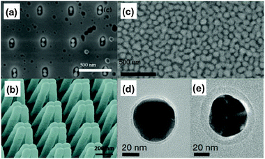 | ||
| Fig. 4 Assembly induced formation of hot spots (a) SEM image of an Au dimer array fabricated by focused ion beam milling and solvent evaporation illustrating the capillary force assembly method. (b) SEM image of Au coated polymer nanofingers in their closed conformation induced by capillary forces structural deformation.(c) SEM image of a monolayer of silica-coated Au nanospheres used in SHINERS. (d), (e) High-resolution TEM images of these nanoparticles, with different shell thicknesses. Parts a and b, reproduced with permission from ref. 49 and 50, respectively, Parts c, d, e reproduced with permission from ref. 55. | ||
Hu et al. have tailored the shape and spacing of nanopillars to control their assembly, and therefore hot spot generation, upon solvent evaporation. Gold nanopillars were fabricated by nanoimprint lithography, providing control of the dimensions as well as the spacing between the pillars. The so-called ‘nanofingers’ were immersed in an ethanolic solution containing analyte molecules. Nanofinger assembly and aggregation is induced by capillary forces upon solvent evaporation. The assembled nanofingers are depicted in Fig. 4b. After drying, the analyte molecules are trapped in between the fingertips, which act as a hot spot. The closed finger samples displayed an increased signal by 10–30× over one without solvent exposure. The authors estimate an EF of 2 × 10¹⁰; however, this value should be approached cautiously due to difficulty in determining molecules in the probe volume. Nonetheless, the results demonstrate a marked increase in signal magnitude through solvent-induced substrate reorganization.50
Another way to circumvent the fact that the Raman probe needs to be located in the vicinity of the electromagnetic hot spot is to build the latter around the target molecule(s), at the interface of two plasmonic surfaces. Taking advantage of technical progress in the domain of SPM, it has been demonstrated that the Raman scattering of a single molecule can be measured when adsorbed on a metallic surface and probed with a metallic tip.52,54 As a result, the field of tip-enhanced Raman scattering (TERS) has developed into a powerful technique for providing molecular information and topography with a resolution of a few nanometres. The configuration for TERS experiments allows the observation of the Raman scattering of single molecules with a control over their location as well as the structure of the hot spot, which is the tip–surface system. As a result, TERS is an invaluable tool for controlling the geometry of the hot spot while achieving single-molecule detection and structural information about the local environment of the molecule.
Inspired by the tip–substrate configuration in TERS, Tian and coworkers designed spherical core–shell nanoparticles to act as ‘tips’—or plasmonic antennas—which can be spread over a surface coated with probe molecules for analysis. This technique is known as shell-isolated nanoparticle-enhanced Raman spectroscopy (SHINERS). The nanoparticles are composed of a Au quasi-spherical core which is encapsulated in very thin (2–4 nm) silica or alumina. When the nanoparticles are deposited over a metallic (Pt) surface functionalised with the Raman probe molecules, enhanced Raman scattering is observed. This is due to the nanoparticle proximity to both the molecules and the surface, resulting in enhanced Raman scattering. Two examples of SHINERS particles are reproduced in Fig. 4d and e.55 It has been previously demonstrated that Raman enhancing efficiency scales as r−10,4,22 yet it is still possible to measure a SERS signal when the nanoparticle and the molecule are a couple of nanometers apart.
The most remarkable result yet in SHINERS is that SERS signals can be measured even when the nanoparticles are spread over non-metallic surfaces, such as a semi-conducting surface (like Si) or even an organic one, such as an orange peel, for the detection of chemicals.55 Substrate generality is an attractive attribute for the SHINERS technique in future sensing and analytical applications. The mechanism for enhancement in SHINERS experiments likely involves electromagnetic coupling between the thin-shell nanoparticles themselves, thereby allowing for overall Raman signal enhancement in the vicinity of the nanoparticles. In this case, the appearance of such hot spots would depend on the surface density of the nanoparticles, yet further studies are required to fully elucidate the intricacies of SHINERS. The precise control over the location of the hot spots is difficult to achieve with SHINERS; however, such systems represent a very significant achievement towards simple-to-use, general, and cost-effective systems for the chemical detection by SERS.
A current challenge in the fabrication of hot spots is the engineering of substrates with a large density of nanometre-scale volumes to fully take advantage of its intrinsic sensitivity for single-molecule detection. Progress from many different angles relating to the production and control over hot spot formation on micro and macroscale substrates has paved the way to larger scale and more highly sensitive SERS-active platforms.
III. Contribution of hot spots to SERS signals
Hot spots play a dominant role in SERS. Although they permit single-molecule detection, the highly dispersive distribution of EFs across a surface can introduce difficulty in the application of SERS to quantitative sensing. In this section, the distribution of EFs on a high performance SERS substrate, the Ag film-over-nanosphere (AgFON), will be examined and its implications to analyte detection and quantitation will be discussed. For accurate and meaningful comparison of the performance of SERS substrates, the EF must be carefully characterized; therefore we describe the calculation of the EF in detail. Finally, the quoted SMSERS EF of 1015 still remains prevalent in the literature in spite of multiple articles and reviews offering more realistic figures.69 Hence, we will discuss the magnitude of the SMSERS EF.III. A. Distribution of enhancement factors and relative contribution to SERS signals
In 2008, Fang, Seong, and Dlott published an elegant report illustrating the distribution of EFs on an AgFON using photon hole burning (PHB).29 Molecules in hot spots experience stronger electromagnetic fields in the near-field and as a result, “burn out” at less intense applied fields. In their work, the intensity of the burning pulse magnified by the EF of the hot spot was carefully chosen to create an electric field near the critical breakdown limit (∼109 V m−1) of molecules on the surface. Increasing laser intensity systematically destroyed molecules on the surface corresponding to locations with decreasingly large EFs. Between burning events, a weak, continuous wave laser probed the SERS intensity originating from the remaining non-damaged molecules on the surface. Using this methodology, it is possible to determine the probability distribution of the EFs and subsequently, the percent contribution of these local EFs to the overall average signal before PHB. The results are exceptional: ∼25% of the SERS signal is generated by less than 0.01% of the molecules on the surface in areas with EFs exceeding 109. The complete dataset illustrating the population and contribution of local enhancement sites is reproduced in Table 2. This EF distribution has wide ranging effects on SERS performance for both sensing and detection applications| Raman enhancement factor | Percentage of molecules | Percent contribution to average SERS signal |
|---|---|---|
| <2.8 × 10⁴ | 0% | 0% |
| 2.8 × 10⁴ to 1 × 10⁵ | 61% | 4% |
| 105 to 106 | 33% | 11% |
| 106 to 107 | 5.1% | 16% |
| 107 to 108 | 0.7% | 22% |
| 108 to 109 | 0.08% | 23% |
| 109 to 1010 | 0.006% | 17% |
| >1010 | 0.0003% | 7% |
The previous analysis depends critically on full monolayer coverage, or more specifically, molecules adsorbed randomly with respect to the spatial hot spot distribution present on the substrate. At sub-monolayer coverage, a spatial distribution of EFs will lead to irreproducible EF values. This is due to analytes randomly sampling different subsets of the EF distribution, and therefore, the resulting signal will be modulated from site to site. In situations where the probe–substrate interaction is dynamic, such as in humid ambient or liquid environments, the distribution of EFs will also lead to spectral fluctuations (a.k.a. blinking) as the analytes diffuse across the surface. In this scenario, the brightest events are likely dominated by a small percentage of the analytes, making EF valuation difficult. Given the intrinsic inhomogeneity of substrates with extremely high EF values, there is a significant advantage to using substrates with a more consistent yet lower average EF for sensing applications over substrates with hot spots. The primary disadvantage to this logic is a higher limit of detection than substrates with hot spots. Another consequence of hot spots is the acceleration of photodegradation processes. Le Ru et al. noted that to measure the highest possible average EF, one must use extremely low laser power (on order nanowatts) to prevent photodamage to analytes in the hot spot.70
Overall, for trace detection and single molecule applications, substrates with hot spots offer significant advantages. The most common substrate employed in SMSERS studies is Ag colloidal aggregates. While these nanoparticle aggregates can harbor some of the highest EF values, they are problematic in terms of consistent sample preparation and SERS activity. To this end, a more consistent and scalable SMSERS-supporting substrate is needed. This seems readily possible as the lowest reported EF for single molecule detection via SERS is 108 for resonant species and 109 for non-resonant analytes on Ag colloids. Although the average EF of an AgFON substrate is lower than this threshold (∼107), it has been previously demonstrated that the maximum EF can be 2 or 3 orders or magnitude greater than the average. It follows that AgFONs are within the EF range necessary to observe SMSERS. An added benefit of rigorously proving SMSERS on a periodic substrate is the generality of this material. Colloids can vary batch to batch, yet a lithographically-fabricated surface has consistent surface properties which can more easily accommodate transfer of knowledge between research groups and applications specialists.
III. B. Reporting a meaningful average EF
Research articles are frequently published reporting a new substrate for SERS, yet it is often difficult to determine the importance of the results as there is no generally-utilized or commonly calculated metric for reporting their performance. The purpose of this section is to outline simple suggestions for calculating the EF of various SERS substrates. This information assists in the comparison of SERS activity between substrates, creating a global setting for the wide variety of potential substrates and allowing their distinct functionality to shine through. In some inaccurate EF reports, not all molecules are accounted for, while in others, resonant molecules such as Rhodamine 6G are compared to non-resonant probes, resulting in artificially large EF with no meaningful indication of the real, physical EF. It is unrealistic that all SERS publications will adopt the same exact methodology to determine the EF, but reports should provide enough detail such that the determined EF has physical meaning and that its magnitude can be understood and compared. In general, there are a few principles in determining the EF that could be adopted by the SERS community:(1) Clearly define how the EF was determined. In its simplest definition, the EFSERS is the ratio of the intensity of the analyte on the surface to a non-surface adsorbed molecule, expressed in eqn 1:
 | (1) |
(2) All molecules on the surface should carry equal weight in the EF calculation. Despite the fact that on some substrates a significant percentage of the signal originates from a small fraction of the total molecules, all molecules on the surface do contribute to the total signal. In ensemble-averaged SERS studies it is ideal to work at surface saturation for EF calculations to limit the effect of random adsorption to hot spots. Additionally, at surface saturation, the most molecules will reside in the hot spots, therefore giving the best-case SERS signal.
(3) It is convenient to use an analyte which is commonly available with well-defined spectroscopy and surface chemistry. For Ag and Au surfaces, thiols are commonly used, specifically thiophenol and its derivatives. Other common molecules used to determine EF include dyes such as Rhodamine 6G, pyridine and 1,2-bis(4-pyridyl)ethylene (BPE). It is especially convenient to use a probe molecule with little fluorescence when excited with the Raman-inducing laser; therefore, the comparison between SERS signal and normal Raman signal can be accomplished using the exact same laser source and other optics, reducing the complexity of the calculation.
It is often challenging to obtain a normal Raman spectrum of the analyte or to quantify the number of molecules adsorbed on a surface, yet these numbers are necessary for an accurate EF evaluation. If a normal Raman spectrum of analyte is not obtainable, it is typically due to overwhelming fluorescence signal or a weak Raman cross section. For example, the most commonly used 532 nm resonant SERS dye, Rhodamine 6G (R6G), has an extremely high fluorescence quantum yield, obscuring any possibility of observing a normal resonance Raman spectrum amidst an overwhelming fluorescence background. In SERS, the fluorescence is quenched by proximity to the metal. In order to determine the EF for fluorescent probe molecules, the resonance Raman cross section must be experimentally determined with stimulated Raman methods,72 or must be estimated by extrapolating the off-resonance Raman cross section.73 Recently, the Etchegoin group extracted Raman signal from a highly fluorescent analyte by careful control of laser polarization.74 The technique is extremely useful yet its facile application requires a great deal of knowledge regarding the molecular and experimental system. For R6G, the difference in Raman cross section between on and off resonance conditions is nearly 106! Another difficulty in measuring INRS may arise from weak Raman scatterers in which no signal is seen without SERS enhancement. In this situation, the Raman cross section may be estimated by theoretical calculations, which may or may not quantitatively disagree with experiment. In some situations it may be possible to obtain INRS on a more sensitive instrument and compare to an internal standard on the SERS apparatus. However, if rigorous measurements of the EF are required and there are difficulties obtaining normal Raman signal, it is likely ideal to switch analytes.
Another challenge in calculating the EF comes from determining the number of molecules contributing to the SERS signal. There are typically uncertainties in surface roughness, surface area, and/or packing densities; therefore, it is best to estimate the maximum possible number of contributing molecules, leading to a lower limit for the SERS EF. If the probe molecules are known to adopt order on a surface then the number of adsorbed molecules should be calculated from the highest possible literature values for packing density. It is also necessary to include a surface roughness factor to account for increased surface area due to the presence of nanostructures.
III. C. Hot spots and SERS enhancement factors in single nanoantennas
SERS nanoantennas, the SiO2 encapsulated cores in Table 1, are an archetypical system to study structure–function relationships in single nanoparticle aggregates with at least one hot spot. Nanoantennas provide stable, long lasting, well-defined morphologies with enough compositional similarity that comparisons between individual nanoantennas can tease out the intricacies of shape and how it relates to enhancing efficiency. A thorough study of SERS nanoantennas was conducted using λex = 633 nm which revealed two types of hot spots present in Au nanoparticle dimers. Fig. 5 shows the interparticle regions between Au cores in dimer nanoantennas. Both nanoantennas were found to have a large SERS EF (∼108) yet one dimer has a gap between particles while the other is formed from coalesced cores with <1 nm local radius of curvature. Hot spots can occur in either structure, which is great for the generality of design rules for SERS substrates. Remarkably, it was found that the EF magnitude was uncorrelated to the spectral position of the LSPR maxima. Additional work examined the range of EFs for a variety of nanoantenna geometries with varying gap sizes. The salient message of this exploration is that there are a number of geometries for aggregates of colloidal particles which all display a significant SERS EF >106 and approaching 109.67 The design rules for SERS substrates are now established. A wide fault tolerance when creating nanostructures for efficient light amplification and localization is demonstrated. This is the best possible outcome—it is easy to fabricate high performance SERS nanoantennas.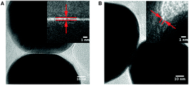 | ||
| Fig. 5 HRTEM images of the interparticle regions between Au cores in dimer nanoantennas. (A) Dimer containing a physical gap with a dgap of ∼0.4 nm (inset). (B) Dimer consisting of coalesced cores (dgap < 0), revealing crevices as small as 0.8 nm (inset). Reproduced with permission from ref. 67. | ||
III. D. The enhancement factor in single molecule SERS
Unfortunately, there has been considerable confusion in the literature about the EFs required for SMSERS as recently discussed by Le Ru et al.71 In the initial SMSERS report,7 the overall cross section of R6G adsorbed to Ag colloid aggregates was measured at 10−14 cm2 per molecule by comparing the intensity to the single molecule fluorescence intensity of the same species. This large cross section was compared to “typical” non-resonant cross sections of 10−30 cm2 per molecule, leading to the estimate of an EF = 1014–15. This comparison is the root of much misinformation in the SMSERS field. The resonance Raman cross section of R6G, integrated over all observable modes with λex = 532 nm, was recently measured by Shim et al. to be 2.3 × 10⁻²² cm2 per molecule, not 10−30 cm2 per molecule.72 If the original SMSERS authors had this piece of data at the time, the EFSERS would have been estimated to be 107. Furthermore, DDA calculations indicate that structures commonly observed in SMSERS can provide, conservatively, enhancements of 108 at 532 nm.3 If the observed cross section is a simple multiplication of the R6G resonance Raman cross section and the electromagnetic SERS EF, the resulting SMSERS cross section is 10−14 cm2 per molecule which is in perfect agreement with the previously reported integrated cross sections of 10−14 cm2 per molecule. As such, the EF in the first SMSERS report is a moderate electromagnetic enhancement coupled with the extraordinarily large resonance Raman cross section of R6G.Recent SMSERS work on another dye molecule, crystal violet, has built upon the previously discussed ideas and provides an example of differentiating the effects of resonant enhancement as well as SERS enhancement. By using a non-fluorescent molecule, we were able to measure INR at λex = 532 nm. These data were then compared with SERS signals from single crystal violet molecules, yielding EF values between 106 and 109. We used theoretical modeling to deconvolute the contribution of resonance Raman enhancement. The difference in cross section between λex = 542 nm and λex = 1064 nm was calculated to be up to 105. This discovery caused us to propose a functional understanding of the total EF to be EFSERRS = EFSERS × EFRR, highlighting the necessity of accounting for all contributions to the observed signal.41
A recent study by the Etchegoin group focused on the photostability of SMSERS probes and how it relates to the observed EF.70 One could imagine that too much field enhancement could cause photodamage to the molecule of interest, and this is precisely what was discovered. By coupling statistical analysis to spectral discrimination this group has been able to accumulate a large inventory of SMSERS spectra on multiple identically-prepared samples while varying laser power. The result is immediately evident upon inspection of Fig. 6. The researchers observed the largest signal intensity, and therefore EF, while using the least amount of laser power. This was rationalized in terms of the photostability of the SMSERS probes, specifically; too much laser power burns out the molecules in the highest enhancing regions. Less laser power allows these molecules to efficiently scatter and the local EF can be determined. This approach has given much insight into the maximum EF as well as the optimal way to determine it.
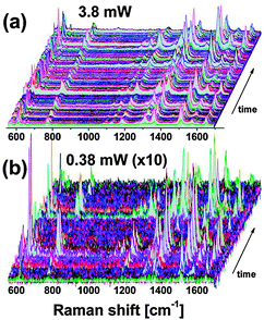 | ||
| Fig. 6 (a) Sequence of 500 spectra taken in colloidal solution at (a) 3.8 mW and (b) 0.38 mW. The intensities in b have been multiplied by 10 to account for the incident power scaling. Both cases are taken with the same integration time (0.2 s). A simple visual inspection of the data reveals qualitatively the effect studied in this paper, that is, in b the events are more sparse (the spectra are also noisier, as expected), but many events (when normalized by the incident power) reach intensities above those displayed in (a). In other words, the maximum intensities are not scaling with power, thus producing events with higher SM-SERS EFs in (b) as compared to (a). The SM-SERS EFs in (a) are restricted by the limited photostability of the molecules. Adapted with permission from ref. 70. | ||
IV. Applications and studies of hot spots
IV.A. Analysis of hot spot geometry using photoactive polymers
The Moerner group performed some of the original experiments on hot spot imaging using a photoactive polymer. They used a commercially available polymer, SU-8, which demonstrates two-photon absorption and polymerization when excited with high fluences of λ = 800 nm light. They found the enhanced field intensities at the tips of triangular nanoantennas promote this nonlinear polymerization. Fig. 7 shows AFM images and line scans across the polymer structures for different laser powers. The lowest power panel demonstrates the best spatial confinement of polymer development, creating less than 30 nm structures.62 It is interesting to note that the Moerner group found growth of polymer (and thus greatest field enhancement) at the tips of each nanostructure, best demonstrated in Fig. 7d, and not in the 36 nm wide gap between them. This demonstrates that much smaller sized gaps are needed to create hot spots between two or more nanoparticles.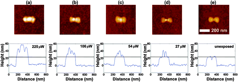 | ||
| Fig. 7 AFM images and cross sections along the nanoantenna axis of bowties exposed at (a) 225 μW, (b) 106 μW, (c) 54 μW, (d) a record low 27 μW, and (e) unexposed bowtie. The black line in the cross-section figures shows the bowtie height before exposure. Each of these bowties has a gap size of 36 nm. Adapted with permission from ref. 62. | ||
The task of imaging the spatial distribution of the enhanced electromagnetic field caused by a hot spot is nontrivial. Recently, Plain and co-workers have used a photoresponsive polymer to topographically image the hot spot distribution on lithographically-patterned silver nanorods as well as triangular nanoantenna structures.75,76 The photoresponsive polymer system is depicted in Fig. 8 and is composed of a photoswitchable azobenzene dye commingled with methylmethacrylate. This polymer system is known to display mass transport as a result of illumination-induced cis–trans isomerization of the azobenzene moiety. The result of the mass transport is a topographic change in the polymer which is responsive to field intensity, gradient, as well as polarization. The researchers use this polymer to image the hot spot as well as generate sub-diffraction limit features in the polymer film.
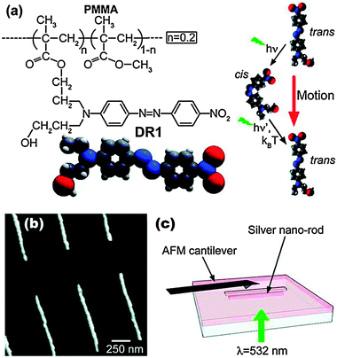 | ||
| Fig. 8 Principle of photopolymerization hot spot imaging. (a) Chemical structure showing the azobenzene grafted to a chain of PMMA and the photoinduced motion via a trans–cis–trans isomerization cycle. (b) Atomic force microscopy image of silver nanorods produced by E-beam lithography. (c) The sample is covered by DR1MA/MMA, laser-illuminated, and characterized by atomic force microscopy. Adapted with permission from ref. 75. | ||
The method of photopolymerization hot spot characterization is as follows: after carefully characterizing the laser intensity threshold for polymerization, the researchers then decrease the laser power to a point where only regions with electromagnetic field enhancement (estimated to be ∼20×) will cross the polymerization threshold. Plain and co-workers have successfully imaged hot spots on bowtie nanoantenna arrays, demonstrating that longitudinally polarized plasmons are confined to the tops of these nanostructures. They further expanded this work to evaluate the temporal fluctuations of hot spots on polycrystalline Ag nanorod samples. Using a photoresponsive polymer gives a real-space representation of the enhanced electromagnetic field and lends insight into the dynamics of hot spot fluctuation.75 This method of qualitative analysis has the potential to provide insights for the better engineering of both single nanoparticle plasmonic materials as well as large-scale templated plasmonic materials.
IV.B. Using SMSERS to elucidate hot spot properties
Extremely large SERS EFs are required to observe the vibrations of single molecules. The nanostructures which support SMSERS provide enormous signal enhancement in a very small region of space. Our research group has utilized correlated HRTEM—LSPR spectroscopy—SMSERS measurements to determine the optical and physical properties of the clusters which support SMSERS.3 We have found no single nanoparticles which support this phenomenon; further, dimers which support SMSERS were comprised of disparately sized nanoparticles. Two examples of SMSERS-supporting aggregates are exhibited in Fig. 9. While dimers seem to be the most easy to fabricate, clusters with higher numbers of particles more commonly support SMSERS.41 In this manner SMSERS has been used to screen for the most enhancing substrates and motifs in substrate geometry which can be integrated into large scale SERS sensing platforms in future work.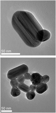 | ||
| Fig. 9 Two examples of aggregates which supported the observation of the vibrational spectrum of single crystal violet isotopologue molecules. Adapted with permission from ref. 41. | ||
SMSERS has also been used to analyze polarization effects with respect to the nanoparticle cluster orientation. It is not currently possible to determine the molecular orientation of a single molecule so most investigations have focused on relationships between the direction of laser polarization and cluster orientation. Nie and co-workers were the first to demonstrate varying SMSERS signal intensities with laser polarization.7 It has been demonstrated that for a dimer, polarization along the ‘long axis’ gives rise to the largest enhancement, shown in Fig. 10. The orthogonal response of the SMSERS signal to laser polarization provides great physical insight into the near-field–far-field coupling for hot spot-containing aggregates. In this example, SMSERS has been used to gain intimate experimental insight into the polarization response for various nanoparticle assemblies.
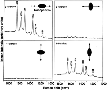 | ||
| Fig. 10 Surface-enhanced Raman spectra of R6G obtained with a linearly polarized confocal laser beam from two Ag nanoparticles. The R6G concentration was 2 × 10⁻¹¹ M, corresponding to an average of 0.1 analyte molecule per particle. The direction of laser polarization and the expected particle orientation are shown schematically for each spectrum. SERS signal is only observed when laser excitation polarization is along the aggregate long axis. Laser wavelength, 514.5 nm; laser power, 250 nW; laser focal radius, 250 nm; integration time, 30 s. All spectra were plotted on the same intensity scale in arbitrary units of the CCD detector readout signal. Adapted with permission from ref. 7. | ||
Recently, the Willets group has used super-resolution imaging to image the spatial origins of SMSERS signals below the diffraction limit of light.77Fig. 11 demonstrates the results of this technique which determines the spatial origin of SERS signals on a sub-diffraction limited length scale. In a subsequent article, the authors use the same technique to elucidate the origins of two optical signals emanating from the system.78 In SERS experiments on a colloidal system there are at least two signals in the Stokes-shifted region of the spectrum—a continuum silver photoluminescence and vibrational bands originating from the adsorbed probe molecule. The researchers found that the blinking of SMSERS signals can be utilized in both the on and off state to detect the spatial origins of the vibrational signal and the photoluminescence background, respectively. They were able to explore some of the intricate details of the hot spot phenomenon through the application of super-resolution imaging techniques, electron microscopy, and DDA calculations. While the entire nanostructure contributes to metal luminescence, the SMSERS signal is localized to a single junction—even if multiple junctions are present. DDA calculations suggested that the origin of metal luminescence is a spatial superposition of all emitting plasmon states and is proportionally related to the square of the electric field. Similarly, the authors demonstrated that agreement between theory and experiment for SMSERS signals requires the calculation to focus on only one nanoparticle junction as the source of Raman enhancement. The theory reproduced the spatial localization of SERS emission by focusing on the fourth power of the electric field; in line with current SERS theory.78 By using this amalgamation of techniques researchers shed light on the physical mechanisms and field-strength dependencies of both metal luminescence and SMSERS signals.
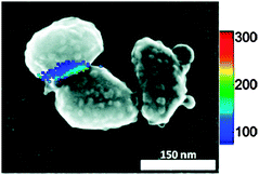 | ||
| Fig. 11 Overlay of the spatial intensity map and SEM image for a SMSERS-supporting nanoparticle aggregate. SMSERS is only observed in the crevice between particles. Adapted with permission from ref. 77. | ||
IV.C. Nonlinear vibrational spectroscopy in hot spots
Enhanced stimulated Raman experiments using plasmonic hot spots have attracted attention since the mid-1970s, when it was proposed that extremely high EFs may be achievable through enhancement of the stimulating field as well as the excitation field.79 Additionally, stimulated Raman techniques have the advantage of being coherent, leading to high collection efficiencies of Raman scattered light as compared to spontaneous Raman techniques. Several efforts were made to examine surface-enhanced Coherent Anti-Stokes Raman Spectroscopy (CARS),80–82 as well as early work on surface-enhanced stimulated Raman gain.83,84 However, in these studies, only a very small portion of the Raman spectrum was examined, and EFs were consistently below 103.One recent successful surface-enhanced nonlinear Raman proof-of-principle experiment, termed SE-FSRS,85 demonstrated EFs of 104–106 using SERS nanoantennas.67,86 These experiments used ground-state femtosecond stimulated Raman spectroscopy85,87 to examine bis-pyridyl ethylene (BPE) molecules adsorbed to SERS nanoantennas, schematically represented in the upper portion of Fig. 12. Using a combination of a picosecond Raman pump pulse and femtosecond Raman probe pulse, coherent stimulated Raman signal spanning a spectral region from 500 to 1800 cm−1 was acquired in several minutes, reproduced in Fig. 12. EFs were estimated to be between 104 and 106, and the nanoparticles were not significantly damaged during irradiation periods much longer than that required to obtain data.
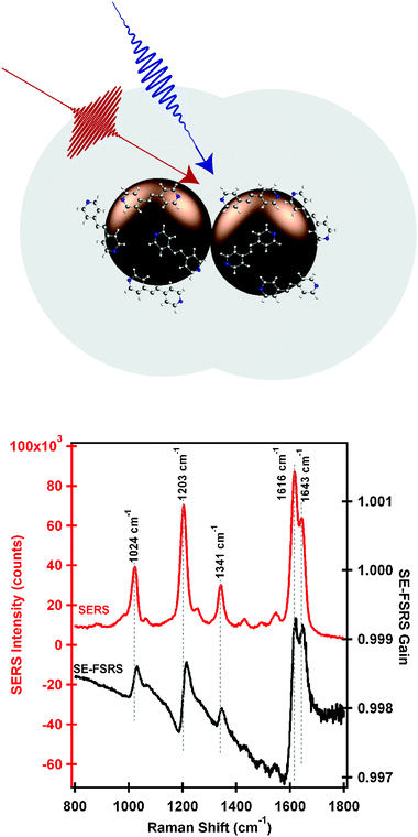 | ||
| Fig. 12 Upper: nanoantennas used for SE-FSRS, consisting of multiple gold cores surrounded by BPE molecules, encapsulated in a silica shell. Lower: SERS spectrum and SE-FSRS spectrum of BPE-functionalized nanoantennas. Both methods obtain high S/N spectra of the well-characterized Raman resonances of BPE, although the SE-FSRS spectrum shows dispersive peaks due to effects from the plasmon. Adapted with permission from ref. 85. | ||
This demonstration of surface-enhanced stimulated Raman spectra predicts the possibility of approaching the single molecule limit with four wave mixing techniques. By examining single molecules using this dynamic technique, or even small homogeneous molecular subsets, one may determine the contributions of environmental heterogeneities in chemical reactions. Additionally, the high S/N data as well as relative ease of experimental setup show that SE-FSRS is a promising approach to observe time-resolved measurements of chemical reaction dynamics in hot spots. By adding an ultrashort photoexcitation pulse, one could observe chemical structural changes with simultaneously high temporal (∼50 fs) and spectral (∼5 cm−1) resolution. Mechanistic details of ultrafast reactions, potentially catalyzed by the electromagnetic fields present in hot spots, could lead to significant understanding of the chemistry of plasmonically catalyzed polymerization, photolithography, photovoltaics, or photocatalysis.
IV. D. Doing chemistry with hot spots
Only a few years after the discovery of SERS, Nitzan and Brus predicted that the concentration of electromagnetic energy resulting from surface plasmon excitation could lead to enhanced photochemistry.88,89 As the electrons are periodically modulated away from the metal surface, it is possible that they are more available for chemistry, particularly affecting molecules near or adsorbed to the surface. However, the possibility of competing processes such as energy transfer from the molecule to the surface, or desorption of molecules, could limit the total enhancement achievable. It logically follows that these effects would be most dramatic in hot spot regions. Additionally, monitoring the mechanistic details of plasmon enhanced photochemistry is achievable using the SERS and SE-FSRS methods described previously. Here we discuss the feasibility of doing chemistry in hot spots in two key areas: (i) photovoltaics, and (ii) photocatalysis.First, plasmonic nanoparticles are extremely efficient light scatterers, thus increasing the path length of photons through a photovoltaic device, leading to increased generation of charge carriers in a given volume.8,96–98 This increase in effective path length allows researchers to reduce cell thickness to match the charge carrier diffusion length, increasing charge collection. A schematic representation of this effect is depicted in Fig. 13. In this scenario, the nanomaterials are simply acting as scattering media, and the presence or absence of hot spots should play no role.
 | ||
| Fig. 13 Increased light scattering in a schematic bulk heterojunction photovoltaic by plasmonic gold nanoparticles. | ||
Secondly, it is thought that the confinement of light and/or the change in electron density distributions due to plasmonic excitation may impact the chemistry of charge generation, exciton quenching, and/or charge recombination in the photovoltaic device. Photoexcitation of a surface plasmon periodically pulls electron density away from the metal's atomic lattice, thus making it more accessible for chemistry. As significant enhancements of the electric field occur in hot spot regions, it is possible that careful tailoring of the region around these sites may lead to increased photovoltaic performance, or simply determine the origin of the plasmonic enhancement. Additionally, excitation of plasmons eventually leads to generation of heat in the surrounding environment; and it is possible that increased temperatures may drive reactions. Ongoing work is currently underway to understand mechanistic details of these processes.
Early work in this field includes a study by Zheng et al. which compared photocatalytic effects with either a roughened silver or polished silver electrode. Their results indicated that the surface plasmon resonance increased the reduction of CO2, potentially by increasing the tunneling probability of a photoexcited electron in the silver to dissolved CO2.110 Similar results were observed for the photoelectrochemical reduction of nitrate on silver surfaces.111 While neither of the aforementioned studies purposefully incorporated hot spot containing nanostructures we believe the incorporation of plasmonic materials with hot spots could allow another mechanism for the enhancement of the photo-mediated process.
More recent work examining the mechanisms of plasmonically improved catalytic rates indicate significant contributions from heating112 as well as increased population of reactant anti-bonding orbitals.113 Further research is clearly needed in order to determine the mechanism of catalytic enhancement; however, it seems likely that the presence of hot spots may favorably alter the probability of occurrence and perhaps the rate of surface chemical reactions. Performing systematic experiments on the photocatalytic rates using the well-characterized plasmonic surfaces described in Section II should further clarify the role of hot spots in these reactions. Additionally, further time-resolved SERS studies, ranging from the femtosecond to second timescales, are needed to determine the mechanistic details of plasmonically enhanced photocatalysis.
V. Conclusion
Through the winding course of topics in this perspective we hope the reader has acquired a more global view of the variety of problems, intricacies, and outlook for hot spots in vibrational spectroscopy and beyond. Based on the proliferation of experimental analysis and computational modeling techniques the once-abstract idea of a hot spot has become a reality. The numerous methods of hot spot generation discussed in this paper have produced a range of colloidal and two-dimensional SERS substrates with widely varying EFs, reproducibility, and yields. We hope that our discussions on the broad distribution of EFs in a given SERS substrate as well as on quantifying enhancement will lead to greater transparency in determining the efficacy of a given substrate compared to others. Additionally, new work in using super-resolution microscopy and other novel experimental techniques to directly measure hot spots is leading to new insight on the distribution of highly localized fields in plasmonic materials; helping to further characterize the range, distribution, and use of these structures. The characterization of such a wide variety of SERS substrates has informed design rules for highly efficient SERS surfaces. Notably, as long as there is a hot spot present, it does not matter if there is a gap or a crevice site. Additionally, it is becoming more clear that perhaps the spectral position of the LSPR does not necessarily dictate the excitation wavelength which will work best for SERS in a hot spot-dominated system.The area of hot spot enhanced photochemical transformations is by far one of the most exciting new areas in plasmonics research. The extreme localization and concentration of electromagnetic fields can, has, and should continue to be exploited in areas of catalysis, drug delivery, ultrafast spectroscopies, and photovoltaics. Future mechanistic studies are needed to determine the exact role of the hot spot in controlling chemistry on the nanoscale; which will be greatly facilitated by further theoretical and experimental work on the fundamental nature of hot spots.
Acknowledgements
The authors gratefully acknowledge support from the following sources: The NSF (CHE-0911145, CHE-0802913 (CaSTL), DMR-0520513). The Department of Basic Energy Sciences (DE-FG02-09ER16109 and DE-FG02-03ER15457). DARPA under SSC Pacific Grant N66001-11-1-4179. Any opinions, findings, and conclusions or recommendations expressed in this publication are those of the authors and do not necessarily reflect the views of DARPA. Nathan Greeneltch is acknowledged for fabricating the substrate show in Fig. 2a.References
- D. L. Jeanmaire and R. P. Van Duyne, J. Electroanal. Chem., 1977, 84, 1–20 CrossRef CAS.
- T. Takenaka, K. Eda, M. Mabuchi, Y. Fujiyoshi and N. Uyeda, Bull. Inst. Chem. Res., Kyoto Univ., 1984, 62, 219–232 CAS.
- J. P. Camden, J. A. Dieringer, Y. Wang, D. J. Masiello, L. D. Marks, G. C. Schatz and R. P. Van Duyne, J. Am. Chem. Soc., 2008, 130, 12616–12617 CrossRef CAS.
- P. L. Stiles, J. A. Dieringer, N. C. Shah and R. P. Van Duyne, Annu. Rev. Anal. Chem., 2008, 1, 601–626 CrossRef CAS.
- K. B. Biggs, J. P. Camden, J. N. Anker and R. P. Van Duyne, J. Phys. Chem. A, 2009, 113, 4581–4586 CrossRef CAS.
- X. Zhang, M. A. Young, O. Lyandres and R. P. Van Duyne, J. Am. Chem. Soc., 2005, 127, 4484–4489 CrossRef CAS.
- S. Nie and S. R. Emory, Science, 1997, 275, 1102–1106 CrossRef CAS.
- H. A. Atwater and A. Polman, Nat. Mater., 2010, 9, 205–213 CrossRef CAS.
- J. A. Schuller, E. S. Barnard, W. Cai, Y. C. Jun, J. S. White and M. L. Brongersma, Nat. Mater., 2010, 9, 193–204 CrossRef CAS.
- K. Kneipp, Y. Wang, H. Kneipp, L. T. Perelman, I. Itzkan, R. R. Dasari and M. S. Feld, Phys. Rev. Lett., 1997, 78, 1667–1670 CrossRef CAS.
- A. M. Michaels, M. Nirmal and L. E. Brus, J. Am. Chem. Soc., 1999, 121, 9932–9939 CrossRef CAS.
- A. M. Michaels, J. Jiang and L. Brus, J. Phys. Chem. B, 2000, 104, 11965–11971 CrossRef CAS.
- E. C. Le Ru, J. Grand, I. Sow, W. R. C. Somerville, P. G. Etchegoin, M. Treguer-Delapierre, G. Charron, N. Felidj, G. Levi and J. Aubard, Nano Lett., 11, 5013–5019 CrossRef CAS.
- Y.-L. Xu, Appl. Opt., 1995, 34, 4573–4588 CrossRef CAS.
- J. McMahon, A.-I. Henry, K. Wustholz, M. Natan, R. Freeman, R. Van Duyne and G. Schatz, Anal. Bioanal. Chem., 2009, 394, 1819–1825 CrossRef CAS.
- J. M. McMahon, S. Li, L. K. Ausman and G. C. Schatz, J. Phys. Chem. C, 2012, 116, 1627–1637 CAS.
- Y. Wang, S. K. Eswaramoorthy, L. J. Sherry, J. A. Dieringer, J. P. Camden, G. C. Schatz, R. P. Van Duyne and L. D. Marks, Ultramicroscopy, 2009, 109, 1110–1113 CrossRef CAS.
- R. Rojas V and F. Claro, J. Chem. Phys., 1993, 98, 998–1006 CrossRef.
- H. Xu, J. Aizpurua, M. Kall and P. Apell, Phys. Rev. E: Stat. Phys., Plasmas, Fluids, Relat. Interdiscip. Top., 2000, 62, 4318–4324 CrossRef CAS.
- S. Zou and G. C. Schatz, Chem. Phys. Lett., 2005, 403, 62–67 CrossRef CAS.
- E. Hao and G. C. Schatz, J. Chem. Phys., 2004, 120, 357–366 CrossRef CAS.
- J. A. Dieringer, A. D. McFarland, N. C. Shah, D. A. Stuart, A. V. Whitney, C. R. Yonzon, M. A. Young, X. Zhang and R. P. Van Duyne, Faraday Discuss., 2006, 132, 9–26 RSC.
- R. P. Van Duyne, J. C. Hulteen and D. A. Treichel, J. Chem. Phys., 1993, 99, 2101–2115 CrossRef CAS.
- T. Lemma and R. F. Aroca, J. Raman Spectrosc., 2002, 33, 197–201 CrossRef CAS.
- J. C. Hulteen, D. A. Treichel, M. T. Smith, M. L. Duval, T. R. Jensen and R. P. Van Duyne, J. Phys. Chem. B, 1999, 103, 3854–3863 CrossRef CAS.
- C. J. Orendorff, L. Gearheart, N. R. Jana and C. J. Murphy, Phys. Chem. Chem. Phys., 2006, 8, 165–170 RSC.
- N. Halas, MRS Bull., 2005, 362–367 CrossRef CAS.
- J. P. Camden, J. A. Dieringer, J. Zhao and R. P. Van Duyne, Acc. Chem. Res., 2008, 41, 1653–1661 CrossRef CAS.
- Y. Fang, N. Seong and D. D. Dlott, Science, 2008, 321, 388–392 CrossRef CAS.
- M. Yang, R. Alvarez-Puebla, H.-S. Kim, P. Aldeanueva-Potel, L. M. Liz-Marzán and N. A. Kotov, Nano Lett., 2010, 10, 4013–4019 CrossRef CAS.
- E. D. Diebold, N. H. Mack, S. K. Doorn and E. Mazur, Langmuir, 2009, 25, 1790–1794 CrossRef CAS.
- E. D. Diebold, P. Peng and E. Mazur, J. Am. Chem. Soc., 2009, 131, 16356–16357 CrossRef CAS.
- L. Gunnarsson, E. J. Bjerneld, H. Xu, S. Petronis, B. Kasemo and M. Kall, Appl. Phys. Lett., 2001, 78, 802–804 CrossRef CAS.
- T. Atay, J.-H. Song and A. V. Nurmikko, Nano Lett., 2004, 4, 1627–1631 CrossRef CAS.
- Q. Yu, P. Guan, D. Qin, G. Golden and P. M. Wallace, Nano Lett., 2008, 8, 1923–1928 CrossRef CAS.
- S. J. Lee, A. R. Morrill and M. Moskovits, J. Am. Chem. Soc., 2006, 128, 2200–2201 CrossRef CAS.
- L. Qin, S. Park, L. Huang and C. A. Mirkin, Science, 2005, 309, 113–115 CrossRef CAS.
- L. Qin, S. Zou, C. Xue, A. Atkinson, G. C. Schatz and C. A. Mirkin, Proc. Natl. Acad. Sci. U. S. A., 2006, 103, 13300–13303 CrossRef CAS.
- D. R. Ward, N. K. Grady, C. S. Levin, N. J. Halas, Y. Wu, P. Nordlander and D. Natelson, Nano Lett., 2007, 7, 1396–1400 CrossRef CAS.
- A. Gopinath, S. V. Boriskina, W. R. Premasiri, L. Ziegler, B. M. Reinhard and L. Dal Negro, Nano Lett., 2009, 9, 3922–3929 CrossRef CAS.
- S. L. Kleinman, E. Ringe, N. Valley, K. L. Wustholz, E. Phillips, K. A. Scheidt, G. C. Schatz and R. P. Van Duyne, J. Am. Chem. Soc., 2011, 133, 4115–4122 CrossRef CAS.
- D.-K. Lim, K.-S. Jeon, H. M. Kim, J.-M. Nam and Y. D. Suh, Nat. Mater., 2010, 9, 60–67 CrossRef CAS.
- D.-K. Lim, K.-S. Jeon, J.-H. Hwang, H. Kim, S. Kwon, Y. D. Suh and J.-M. Nam, Nat. Nanotechnol., 2011, 6, 452–460 CrossRef CAS.
- N. H. Kim, S. J. Lee and M. Moskovits, Adv. Mater., 2011, 23, 4152–4156 CrossRef CAS.
- H. Gehan, L. Fillaud, M. M. Chehimi, J. Aubard, A. Hohenau, N. Felidj and C. Mangeney, ACS Nano, 2010, 4, 6491–6500 CrossRef CAS.
- R. A. Álvarez-Puebla, R. Contreras-Cáceres, I. Pastoriza-Santos, J. Pérez-Juste and L. M. Liz-Marzán, Angew. Chem., Int. Ed., 2009, 48, 138–143 CrossRef.
- W. Doering, M. Piotti, M. Natan and R. Freeman, Adv. Mater., 2007, 19, 3100–3108 CrossRef CAS.
- S. E. A. Gratton, S. S. Williams, M. E. Napier, P. D. Pohlhaus, Z. Zhou, K. B. Wiles, B. W. Maynor, C. Shen, T. Olafsen, E. T. Samulski and J. M. DeSimone, Acc. Chem. Res., 2008, 41, 1685–1695 CrossRef CAS.
- K. D. Alexander, M. J. Hampton, S. Zhang, A. Dhawan, H. Xu and R. Lopeza, J. Raman Spectrosc., 2009, 40, 2171–2175 CrossRef CAS.
- M. Hu, F. S. Ou, W. Wu, I. Naumov, X. Li, A. M. Bratkovsky, R. S. Williams and Z. Li, J. Am. Chem. Soc., 2010, 132, 12820–12822 CrossRef CAS.
- F. S. Ou, M. Hu, I. Naumov, A. Kim, W. Wu, A. M. Bratkovsky, X. Li, R. S. Williams and Z. Li, Nano Lett., 2011, 11, 2538–2542 CrossRef CAS.
- K. F. Domke, D. Zhang and B. Pettinger, J. Am. Chem. Soc., 2006, 128, 14721–14727 CrossRef CAS.
- C. C. Neacsu, J. Dreyer, N. Behr and M. B. Raschke, Phys. Rev. B: Condens. Matter, 2006, 73, 193406 CrossRef.
- M. D. Sonntag, J. M. Klingsporn, L. K. Garibay, J. M. Roberts, J. A. Dieringer, T. Seideman, K. A. Scheidt, L. Jensen, G. C. Schatz and R. P. Van Duyne, J. Phys. Chem. C, 2012, 116, 478–483 CAS.
- J. F. Li, Y. F. Huang, Y. Ding, Z. L. Yang, S. B. Li, X. S. Zhou, F. R. Fan, W. Zhang, Z. Y. Zhou, D. Y. Wu, B. Ren, Z. L. Wang and Z. Q. Tian, Nature, 2010, 464, 392–395 CrossRef CAS.
- J. R. Anema, J.-F. Li, Z.-L. Yang, B. Ren and Z.-Q. Tian, Annu. Rev. Anal. Chem., 2011, 4, 129–150 CrossRef CAS.
- M. Yang, R. Alvarez-Puebla, H.-S. Kim, P. Aldeanueva-Potel, L. M. Liz-Marzán and N. A. Kotov, Nano Lett., 2010, 10, 4013–4019 CrossRef CAS.
- L. Rodríguez-Lorenzo, R. A. Álvarez-Puebla, F. J. G. de Abajo and L. M. Liz-Marzán, J. Phys. Chem. C, 2010, 114, 7336–7340 Search PubMed.
- L. Rodríguez-Lorenzo, R. n. A. Álvarez-Puebla, I. Pastoriza-Santos, S. Mazzucco, O. Stéphan, M. Kociak, L. M. Liz-Marzán and F. J. García de Abajo, J. Am. Chem. Soc., 2009, 131, 4616–4618 CrossRef.
- X. S. Shen, G. Z. Wang, X. Hong and W. Zhu, Phys. Chem. Chem. Phys., 2009, 11, 7450–7454 RSC.
- J. Theiss, P. Pavaskar, P. M. Echternach, R. E. Muller and S. B. Cronin, Nano Lett., 2010, 10, 2749–2754 CrossRef CAS.
- A. Sundaramurthy, P. J. Schuck, N. R. Conley, D. P. Fromm, G. S. Kino and W. E. Moerner, Nano Lett., 2006, 6, 355–360 CrossRef CAS.
- D. Graham, D. G. Thompson, W. E. Smith and K. Faulds, Nat. Nanotechnol., 2008, 3, 548–551 CrossRef CAS.
- R. W. Taylor, T.-C. Lee, O. A. Scherman, R. Esteban, J. Aizpurua, F. M. Huang, J. J. Baumberg and S. Mahajan, ACS Nano, 5, 3878–3887 CrossRef CAS.
- J. A. Dieringer, R. B. Lettan, K. A. Scheidt and R. P. Van Duyne, J. Am. Chem. Soc., 2007, 129, 16249–16256 CrossRef CAS.
- S. E. J. Bell and M. R. McCourt, Phys. Chem. Chem. Phys., 2009, 11, 7455–7462 RSC.
- K. L. Wustholz, A. I. Henry, J. M. McMahon, R. G. Freeman, N. Valley, M. E. Piotti, M. J. Natan, G. C. Schatz and R. P. Van Duyne, J. Am. Chem. Soc., 2010, 132, 10903–10910 CrossRef CAS.
- M. Roca and A. J. Haes, J. Am. Chem. Soc., 2008, 130, 14273–14279 CrossRef CAS.
- E. C. Le Ru, P. G. Etchegoin and M. Meyer, J. Chem. Phys., 2006, 125, 204701 CrossRef CAS.
- P. G. Etchegoin, P. D. Lacharmoise and E. C. Le Ru, Anal. Chem., 2009, 81, 682–688 CrossRef CAS.
- E. C. Le Ru, E. Blackie, M. Meyer and P. G. Etchegoin, J. Phys. Chem. C, 2007, 111, 13794–13803 CAS.
- S. Shim, C. M. Stuart and R. A. Mathies, ChemPhysChem, 2008, 9, 697–699 CrossRef CAS.
- S. A. Meyer, E. C. Le Ru and P. G. Etchegoin, J. Phys. Chem. A, 2010, 114, 5515–5519 CrossRef CAS.
- E. C. Le Ru, L. C. Schroeter and P. G. Etchegoin, Anal. Chem., 2012, 84, 5074–5079 CrossRef CAS.
- M. L. Juan, J. Plain, R. Bachelot, A. Vial, P. Royer, S. K. Gray, J. M. Montgomery and G. P. Wiederrecht, J. Phys. Chem. A, 2009, 113, 4647–4651 CrossRef CAS.
- C. Hubert, R. Bachelot, J. Plain, S. Kostcheev, G. Lerondel, M. Juan, P. Royer, S. Zou, G. C. Schatz, G. P. Wiederrecht and S. K. Gray, J. Phys. Chem. C, 2008, 112, 4111–4116 CAS.
- S. M. Stranahan and K. A. Willets, Nano Lett., 2010, 10, 3777–3784 CrossRef CAS.
- M. L. Weber, J. P. Litz, D. J. Masiello and K. A. Willets, ACS Nano, 2012, 6, 1839–1848 CrossRef CAS.
- H. Chew, D. S. Wang and M. Kerker, J. Opt. Soc. Am. B, 1984, 1, 56–66 CrossRef CAS.
- E. J. Liang, A. Weippert, J. M. Funk, A. Materny and W. Kiefer, Chem. Phys. Lett., 1994, 227, 115–120 CrossRef CAS.
- T. Ichimura, N. Hayazawa, M. Hashimoto, Y. Inouye and S. Kawata, J. Raman Spectrosc., 2003, 34, 651–654 CrossRef CAS.
- V. Namboodiri, M. Namboodiri, G. I. Cava Diaz, M. Oppermann, G. Flachenecker and A. Materny, Vib. Spectrosc., 2011, 56, 9–12 CrossRef CAS.
- J. P. Heritage, J. G. Bergman, A. Pinczuk and J. M. Worlock, Chem. Phys. Lett., 1979, 67, 229–232 CrossRef CAS.
- B. F. Levine, C. V. Shank and J. P. Heritage, IEEE J. Quantum Electron., 1979, 15, 1418–1432 CrossRef.
- R. R. Frontiera, A.-I. Henry, N. L. Gruenke and R. P. Van Duyne, J. Phys. Chem. Lett., 2011, 2, 1199–1203 CrossRef CAS.
- T. P. Tyler, A.-I. Henry, R. P. Van Duyne and M. C. Hersam, J. Phys. Chem. Lett., 2011, 2, 218–222 CrossRef CAS.
- P. Kukura, D. W. McCamant and R. A. Mathies, Annu. Rev. Phys. Chem., 2007, 58, 461–488 CrossRef CAS.
- A. Nitzan and L. E. Brus, J. Chem. Phys., 1981, 75, 2205–2214 CrossRef CAS.
- A. Nitzan and L. E. Brus, J. Chem. Phys., 1981, 74, 5321–5322 CrossRef CAS.
- D. H. Wang, D. Y. Kim, K. W. Choi, J. H. Seo, S. H. Im, J. H. Park, O. O. Park and A. J. Heeger, Angew. Chem., Int. Ed., 2011, 50, 5519–5523 CrossRef CAS.
- J. L. Wu, F. C. Chen, Y. S. Hsiao, F. C. Chien, P. L. Chen, C. H. Kuo, M. H. Huang and C. S. Hsu, ACS Nano, 2011, 5, 959–967 CrossRef CAS.
- M. D. Brown, T. Suteewong, R. S. S. Kumar, V. D'Innocenzo, A. Petrozza, M. M. Lee, U. Wiesner and H. J. Snaith, Nano Lett., 2011, 11, 438–445 CrossRef CAS.
- B. P. Rand, P. Peumans and S. R. Forrest, J. Appl. Phys., 2004, 96, 7519–7526 CrossRef CAS.
- R. A. Pala, J. White, E. Barnard, J. Liu and M. L. Brongersma, Adv. Mater., 2009, 21, 3504–3509 CrossRef CAS.
- F. J. Beck, A. Polman and K. R. Catchpole, J. Appl. Phys., 2009, 105, 114310 CrossRef.
- O. Stenzel, A. Stendal, K. Voigtsberger and C. Vonborczyskowski, Sol. Energy Mater. Sol. Cells, 1995, 37, 337–348 CrossRef CAS.
- K. R. Catchpole and A. Polman, Appl. Phys. Lett., 2008, 93, 191113 CrossRef.
- K. R. Catchpole and A. Polman, Opt. Express, 2008, 16, 21793–21800 CrossRef CAS.
- T. Hirakawa and P. V. Kamat, J. Am. Chem. Soc., 2005, 127, 3928–3934 CrossRef CAS.
- A. Primo, A. Corma and H. Garcia, Phys. Chem. Chem. Phys., 2010, 13, 886–910 RSC.
- D. B. Ingram and S. Linic, J. Am. Chem. Soc., 2011, 133, 5202–5205 CrossRef CAS.
- Z. W. Liu, W. B. Hou, P. Pavaskar, M. Aykol and S. B. Cronin, Nano Lett., 2011, 11, 1111–1116 CrossRef CAS.
- W. H. Hung, M. Aykol, D. Valley, W. B. Hou and S. B. Cronin, Nano Lett., 2010, 10, 1314–1318 CrossRef CAS.
- K. Mori, M. Kawashima, M. Che and H. Yamashita, Angew. Chem., Int. Ed., 2010, 49, 8598–8601 CrossRef CAS.
- M. Murdoch, G. I. N. Waterhouse, M. A. Nadeem, J. B. Metson, M. A. Keane, R. F. Howe, J. Llorca and H. Idriss, Nat. Chem., 2011, 3, 489–492 CAS.
- I. M. Arabatzis, T. Stergiopoulos, M. C. Bernard, D. Labou, S. G. Neophytides and P. Falaras, Appl. Catal., B, 2003, 42, 187–201 CrossRef CAS.
- K. Awazu, M. Fujimaki, C. Rockstuhl, J. Tominaga, H. Murakami, Y. Ohki, N. Yoshida and T. Watanabe, J. Am. Chem. Soc., 2008, 130, 1676–1680 CrossRef CAS.
- W. B. Hou, Z. W. Liu, P. Pavaskar, W. H. Hung and S. B. Cronin, J. Catal., 2011, 277, 149–153 CrossRef CAS.
- M. V. Dozzi, L. Prati, P. Canton and E. Selli, Phys. Chem. Chem. Phys., 2009, 11, 7171–7180 RSC.
- J. W. Zheng, T. H. Lu, T. M. Cotton and G. Chumanov, J. Electroanal. Chem., 2002, 518, 6–12 CrossRef CAS.
- J. W. Zheng, T. H. Lu, T. M. Cotton and G. Chumanov, J. Phys. Chem. B, 1999, 103, 6567–6572 CrossRef CAS.
- J. R. Adleman, D. A. Boyd, D. G. Goodwin and D. Psaltis, Nano Lett., 2009, 9, 4417–4423 CrossRef CAS.
- P. Christopher, H. L. Xin and S. Linic, Nat. Chem., 2011, 3, 467–472 CAS.
| This journal is © the Owner Societies 2013 |