 Open Access Article
 This Open Access Article is licensed under a Creative Commons Attribution-Non Commercial 3.0 Unported Licence
An unsymmetrical pentacene derivative with ambipolar behavior in organic thin-film transistors†
Sebastian H.
Etschel
ab,
Andreas R.
Waterloo
a,
Johannes T.
Margraf‡
c,
Atefeh Y.
Amin
b,
Frank
Hampel
a,
Christof M.
Jäger
c,
Timothy
Clark
c,
Marcus
Halik
*b and
Rik R.
Tykwinski
*a
aFriedrich-Alexander-Universität Erlangen-Nürnberg, Department of Chemistry and Pharmacy & Interdisciplinary Center of Molecular Materials (ICMM), Henkestraße 42, 91054 Erlangen, Germany. E-mail: rik.tykwinski@chemie.uni-erlangen.de; Fax: +49 9131 85 26865; Tel: +49 9131 85 22540
bFriedrich-Alexander-Universität Erlangen-Nürnberg, Institute of Polymer Materials, Organic Materials and Devices, Martenstraße 7, 91058 Erlangen, Germany. E-mail: marcus.halik@ww.uni-erlangen.de; Fax: +49 9131 85 28321; Tel: +49 9131 85 27732
cFriedrich-Alexander-Universität Erlangen-Nürnberg, Computer Chemie Centrum, Nägelsbachstraße 25, 91052 Erlangen, Germany. E-mail: clark@chemie.uni-erlangen.de; Fax: +49 9131 85 26565; Tel: +49 9131 85 22948
First published on 24th May 2013
Abstract
Three new unsymmetrical anthracenyl-pentacene derivatives have been synthesized, characterized using X-ray crystallography, and used as semiconductors in OTFTs. For one derivative, ambipolar charge carrier transport was observed with a hole mobility of 0.2 cm2 V−1 s−1 and an electron mobility of 0.03 cm2 V−1 s−1.
Organic π-conjugated systems are promising materials for use in organic thin-film transistors (OTFTs).1 Linear acenes, such as pentacene and its derivatives, are prominent examples.2–4 Hole mobilities greater than 1 cm2 V−1 s−1 have been reported for OTFTs using 6,13-bis(triisopropylsilylethynyl)pentacene as a solution processed semiconductor.4,5 The high charge carrier mobility of this derivative has been attributed to effective 2D π-stacking in the crystalline state.3,6,7 Recent synthetic efforts have also yielded pentacene derivatives with pendent ethynylarene groups designed to increase the active π-surface of the system.8 The ethynyl spacer separates the pentacene core from the arene substituent and allows for a coplanar geometry of the two acenes. In contrast, removing the ethynyl spacer between the two chromophores would give a system in which the π-system of the pentacene and the appended aryl group are orthogonally arranged due to steric interactions (Scheme 1). It was predicted that the orthogonal orientation of the two chromophores might improve the intermolecular electronic coupling in different spacial dimensions, giving useful semiconductors for incorporation into OTFTs.9 Guided by this hypothesis, we report the synthesis, characterization, crystal structure analysis, and OTFT devices of a new series of pentacene derivatives 1a–c.
 | ||
| Scheme 1 Synthesis of pentacene derivatives 1a–c. | ||
Pentacene derivatives 1a–c were obtained by the reaction of lithiated anthracenes 2a,b10 with either ketone 3a or 3b,11 followed by reductive elimination with SnCl2·2H2O. Yields obtained over the two steps were respectable (see ESI† for details).
X-ray crystallographic analysis of 1a–c shows that the anthracene and pentacene groups are nearly orthogonal (torsional angles of 84–90°). The packing of 1a shows 2D π-stacking of the pentacenes (Fig. 1a). In addition, the anthracene substituents show 1D π-stacking perpendicular to the 2D pentacene bricklayer (see ESI†). Compound 1b, on the other hand, shows only 1D slipped stacks with interplanar distances of ca. 3.3 and 4.1 Å (Fig. 1b) (see ESI†). Finally, compound 1c shows a 1D pattern with very little π-overlap, and neighbouring 1D stacks are oriented 180° relative to each other (Fig. 1c). This alternate arrangement is likely due to the electronic influence of the fluorine substituent, through increased dipolar interactions and intermolecular edge-to-face interactions (ESI†).
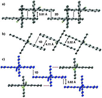 | ||
| Fig. 1 Crystal structures of 1a–c; (a) 2D brick-wall pattern of 1a; (b) 1D slipped stack packing of 1b; (c) 1D slipped stacks of 1c (blue), in which edge-to-face/face-to-face interactions between stacks are highlighted by red/black lines (silyl substituents omitted for clarity). | ||
The absorption spectra of 1a–c are nearly identical in the low energy region, showing three peaks at ca. 536, 574, and 622 nm, characteristic of the pentacene chromophore (see ESI†) and confirming the absence of electronic communication between the anthracene and pentacene groups.12 Likewise, the optical band gap (Eoptgap) of 1a–c, as estimated from the cutoff of the longest wavelength absorption peak (λoffmax), shows little variance (Table 1, see ESI† for details).
| Derivative | HOMOa (eV) | LUMOa (eV) |
E
elgap![[thin space (1/6-em)]](https://www.rsc.org/images/entities/char_2009.gif) a (eV) a (eV) |
E
optgapb (eV) |
λ
offmaxc (nm) |
|---|---|---|---|---|---|
| a Determined using CV. b Determined using absorption spectroscopy (see ESI). c Determined using the intercept of the tangent applied to the longest wavelength absorption peak and the baseline. | |||||
| 1a | −5.17 | −3.21 | 1.96 | 1.92 | 645 |
| 1b | −5.16 | −3.19 | 1.97 | 1.93 | 644 |
| 1c | −5.17 | −3.16 | 2.01 | 1.93 | 643 |
Cyclic voltammetry (CV) has been used to estimate the energy of the highest occupied and the lowest unoccupied molecular orbitals (HOMO and LUMO, respectively, see ESI†) and the electrical band gap (Eelgap), as summarized in Table 1. There is only a minor influence of structural changes on the redox behavior of 1a–c, suggesting that both the HOMO and the LUMO are fully located on the pentacene chromophore, with little contribution from the anthracene substituent. This premise has also been confirmed by calculations (vide infra).
Thin films of 1a–c were incorporated by thermal evaporation into OTFT devices with a bottom-gate–top-contact architecture using doped Si wafers with a 100 nm layer of thermally grown SiO2 as substrates. A thin layer (20 nm) of 1a–c was evaporated directly onto the SiO2 gate dielectric. The Au source and drain electrodes were then defined by thermal evaporation (30 nm) through a stencil mask. Hole mobilities measured for 1a–c in the saturation regime were on the order of μh = 10−7 cm2 V−1 s−1 for devices measured in a glove-box (Table 2, threshold voltages (Vth), current on/off ratios (Ion/Ioff), and the drain to gate current ratios (ID/IG) are summarized in the ESI†). Finally, no n-type behavior was observed for devices on Si/SiO2 substrates, as expected due to the trapping of electrons by the reactive SiO2 dielectric.13
| Derivativea | μ h (Si/SiO2)b | μ h (AlOx–C14PA)b | μ el (ALOx–C14PA)b |
|---|---|---|---|
| a Vapor phase deposition of 1a–c onto the corresponding substrate. b Devices measured in the glove-box under N2. c L = 100 μm. d L = 60 μm; W = 500 μm for all OTFTs. | |||
| 1a | 1.2 × 10⁻⁷c |
— | — |
| 1b | 7.1 × 10⁻⁷c |
1.8 × 10⁻²d |
— |
| 1c | 6.8 × 10⁻⁷c |
1.6 × 10⁻¹d |
7.6 × 10⁻³d |
In order to achieve lower operating voltages for the OTFT devices and to provide a low surface energy interface, which often leads to improved molecular order,14 the setup of the OTFT was changed (Fig. 2a).15,16 Aluminum gate electrodes were evaporated onto a Si/SiO2 wafer and patterned by a shadow mask. Subsequent oxidation in O2 plasma yielded an AlOx layer, approximately 3.6 nm thick.17 The substrate was then immersed in a 0.2–0.3 mM solution of tetradecylphosphonic acid (C14PA) in iso-propanol, which formed a self-assembled monolayer (SAM), yielding an AlOx–C14PA hybrid dielectric with a gate capacitance of 0.72 μF cm−2 (see ESI†). Semiconductors 1a–c were then evaporated onto the AlOx–C14PA hybrid dielectric, followed by the Au source and drain electrodes. Semiconductor 1a on the AlOx–C14PA hybrid dielectric did not yield working OTFTs, which has been attributed to an incongruous semiconductor layer on the low surface energy dielectric (see ESI†). On the other hand, 1b and 1c yielded homogeneous thin-films with connected grains on the SAM surface. These devices exhibited hole mobilities up to μh = 0.05 and 0.2 cm2 V−1 s−1, respectively, for 1b and 1c, with a maximum applied driving voltage of 2.5 V (Table 2). Thus, mobilities are improved by more than five orders of magnitude compared to devices on the Si/SiO2 substrate. At the same time, Vth was reduced from approximately 10 V to 2 V (see ESI† for details). Additionally, electron transport was obtained for 1c, with mobility μel = 0.03 cm2 V−1 s−1.
 | ||
| Fig. 2 (a) Schematic representation of the TFT setup using the AlOx–C14PA hybrid dielectric; (b) output (green) and transfer (blue/red) characteristics of 1c in the saturation regime. | ||
To characterize the nature of the semiconducting properties of 1a–c, semiempirical AM118 calculations were performed on nanocrystals, derived from experimental single-crystal X-ray analyses using EMPIRE (each consisting of >11000 atoms).19 Electron- and hole-transport pathways can be visualized from the local electron affinity (EAL) and ionization potential (IEL),20 respectively, via a Monte Carlo path search algorithm. The lowest barrier (and therefore most likely) electron pathways involve mainly the π-systems of the pentacene stacks (Fig. 3a–c) via face-to-face interactions that lead to anisotropic transport behavior. Additional low barrier pathways involving a combination of pentacene and anthracene transitions are found only for 1c (Fig. 3d). On the other hand, hole-transfer pathways favor sites along the edges of the molecules (Fig. 3e–g). The trends found for the energy barriers along these pathways correspond qualitatively to those found for the observed hole mobilities (36.2, 55.9 and 47.8 kcal mol−1 for 1a–c respectively), indicating that hole mobilities are governed by the activated charge transport from molecule to molecule. Electron transfer barriers follow the same trend (55.4, 88.9 and 86.9 kcal mol−1) and are significantly higher, as reflected in the preferred p-type behavior of all devices.
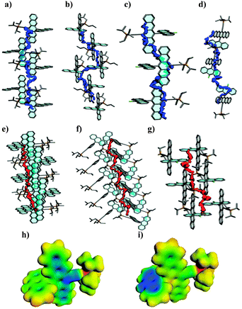 | ||
| Fig. 3 Electron transfer pathways for (a) 1a, (b) 1b, and (c and d) 1c. Hole transfer pathways for (e) 1a, (f) 1b, and (g) 1c. (h) Molecular electrostatic potential (MEP) mapped on the electron density isosurface of the 1c radical anion, and (i) MEP mapped on the first excited state of the 1c radical anion (MEP maps: electron density isovalue is 0.017 e−1 Å−3, potentials are mapped from −0.45 (blue) to 0.1 (red) Ha e−1). | ||
An obvious question is whether fluorination in 1c has an effect beyond changing the crystal structure.21 Calculations of the excitation energies of individual molecules in vacuo show that fluorination significantly decreases the first doublet excitation energy of the radical anion (1a = 1.648 eV; 1b = 1.651 eV; 1c = 1.536 eV). UNO-CIS molecular electrostatic potential maps (calculated using VAMP 11.022) of the ground and excited states show that this process involves a shift of negative charge density to the anthracene group (Fig. 3h and i).23 In other words, fluorination facilitates the participation of the anthracene unit in electron transport.
In summary, we have reported a series of anthracenyl-pentacene derivatives 1a–c, which show orthogonal arrangement of the two π-systems. Using a low surface energy AlOx–C14PA hybrid gate dielectric increases hole mobilities by five orders of magnitude for 1b and 1c relative to Si/SiO2 devices. Additionally, electron transport is observed for 1c, which is attributed to the fluorination of the anthracene substituent in 1c.
Notes and references
- B. Lucas, T. Trigaud and C. Videlot-Ackermann, Polym. Int., 2012, 61, 374–389 CrossRef CAS.
- F. Würthner, Angew. Chem., Int. Ed., 2001, 40, 1037–1039 CrossRef.
- J. E. Anthony, Angew. Chem., Int. Ed., 2008, 47, 452–483 CrossRef CAS.
- F. Yakuphanoglu and B. Gunduz, Synth. Met., 2012, 162, 1210–1239 CrossRef CAS.
- S. K. Park, T. N. Jackson, J. E. Anthony and D. A. Mourey, Appl. Phys. Lett., 2007, 91, 63514 CrossRef.
- J. E. Anthony, J. S. Brooks, D. L. Eaton and S. R. Parkin, J. Am. Chem. Soc., 2001, 123, 9482–9483 CrossRef CAS.
- D. Lehnherr and R. R. Tykwinski, Materials, 2010, 3, 2772–2800 CrossRef CAS.
- D. Lehnherr, A. H. Murray, R. McDonald, M. J. Ferguson and R. R. Tykwinski, Chem.–Eur. J., 2009, 15, 12580–12584 CrossRef CAS.
- X. Zhang, X. Jiang, J. Luo, C. Jing, C. Chunyan, H. Chen and J. Wu, Chem.–Eur. J., 2010, 16, 464–468 CrossRef CAS.
- L. Zhu, R. O. Al-Kaysi, R. J. Dillon, F. S. Tham and C. J. Bardeen, Cryst. Growth Des., 2011, 11, 4975–4983 CAS.
- D. Lehnherr, A. H. Murray, R. McDonald and R. R. Tykwinski, Angew. Chem., Int. Ed., 2010, 49, 6190–6194 CrossRef CAS; D. Lehnherr, J. Gao, F. A. Hegman and R. R. Tykwinski, Org. Lett., 2008, 10, 4779–4782 CrossRef.
- A. R. Waterloo, S. Kunakom, F. Hampel and R. R. Tykwinski, Macromol. Chem. Phys., 2012, 213, 1020–1032 CrossRef CAS.
- L.-L. Chua, J. Zaumseil, J.-F. Chang, E. C.-W. Ou, P. K.-H. Ho, H. Sirringhaus and R. H. Friend, Nature, 2005, 434, 194–199 CrossRef CAS.
- A. Y. Amin, A. Khassanov, K. Reuter, T. Meyer-Friedrichsen and M. Halik, J. Am. Chem. Soc., 2012, 134, 16548–16550 CrossRef CAS.
- M. Halik, H. Klauk, U. Zschieschang, G. Schmid, C. Dehm, M. Schütz, S. Maisch, F. Effenberger, M. Brunnbauer and F. Stellacci, Nature, 2004, 431, 963–966 CrossRef CAS.
- C. Boulas, J. V. Davidovits, F. Rondelez and D. Vuillaume, Phys. Rev. Lett., 1996, 76, 4797–4800 CrossRef CAS.
- M. Novak, A. Ebel, T. Meyer-Friedrichsen, A. Jedaa, B. F. Vieweg, G. Yang, K. Voitchovsky, F. Stellacci, E. Spiecker, A. Hirsch and M. Halik, Nano Lett., 2011, 11, 156–159 CrossRef CAS.
- M. J. S. Dewar, E. G. Zoebisch, E. F. Healy and J. J. P. Stewart, J. Am. Chem. Soc., 1985, 107, 3902–3909 CrossRef CAS.
- T. Clark and M. Hennemann, EMPIRE'12, Erlangen, 2011 Search PubMed.
- B. Ehresmann, B. Martin, A. H. C. Horn and T. Clark, J. Mol. Model, 2003, 9, 342–347 CrossRef CAS.
- For discussion of crystal engineering related to acene performance, see: (a) C. R. Swartz, S. R. Parkin, J. E. Bullock, J. E. Anthony, A. C. Mayer and G. G. Malliaras, Org. Lett., 2005, 7, 3163–3166 CrossRef CAS; (b) F. Würthner and R. Schmidt, ChemPhysChem, 2006, 7, 793–797 CrossRef.
- T. Clark, A. Alex, B. Beck, F. Burkhardt, J. Chandrasekhar, P. Gedeck, A. Horn, M. Hutter, B. Martin, P. O. Dral, G. Rauhut, W. Sauer, T. Schindler and T. Steinke, VAMP 11.0, Erlangen, 2011 Search PubMed.
- P. O. Dral and T. Clark, J. Phys. Chem. A, 2011, 115, 11303–11312 CrossRef CAS.
Footnotes |
| † Electronic supplementary information (ESI) available. CCDC 927705–927707. For ESI and crystallographic data in CIF or other electronic format see DOI: 10.1039/c3cc43270j |
| ‡ J. T. Margraf is supported by the Beilstein Foundation. |
| This journal is © The Royal Society of Chemistry 2013 |