 Open Access Article
 This Open Access Article is licensed under a Creative Commons Attribution-Non Commercial 3.0 Unported Licence
Fabrication and size dependent properties of porous silicon nanotube arrays†
Xuezhen Huanga, Roberto Gonzalez-Rodrigueza, Ryan Richb, Zygmunt Gryczynskib and Jeffery L. Coffer*a
aDepartment of Chemistry, Texas Christian University, Fort Worth, TX 76129, USA. E-mail: j.coffer@tcu.edu; Fax: +1 817 257 5851; Tel: +1 817 257 6223
bDepartment of Physics, Texas Christian University, Fort Worth, TX 76129, USA
First published on 14th May 2013
Abstract
A general method for the formation of a broad family of silicon nanotube arrays (Si NTAs) relevant to diverse fields – ranging from energy storage to therapeutic platforms – is described. Such nanotubes demonstrate a thickness-dependent dissolution behavior important to its potential use in drug delivery. Under selected conditions, novel porous silicon nanotubes can be prepared when the shell thickness is on the order of 12 nm or less, capable of being loaded with small molecules such as luminescent ruthenium dyes associated with dye-sensitized photovoltaic devices.
Semiconductor nanotubes (NTs) such as those comprised of silicon (Si) are attractive experimental targets because of their promising potential in applications in photovolatics, battery technology, hydrogen storage, as well as extending into the realm of nanoscale drug delivery.1–4 While of theoretical interest for some time,5 few routes to formation of silicon nanotubes have actually been achieved experimentally.1 Routes explored to date often rely on incomplete filing of a porous alumina template, a process that is very difficult to control with product uniformity, as it is easy to overfill a given pore and produce solid nanowire structures. Another reported route employs gas phase condensation, a process that yields a large amount of amorphous, ill-defined particles and only a few nanotubes on a given surface.6 Thus it remains a challenge to produce relatively large area nanotube arrays in a straightforward manner, with sensitive control over feature size and composition, thereby permitting an analysis of size-dependent properties.
More recent investigations have identified templating methods based on ZnO nanowire7,8 (NW) or Ge NW9 cores as a promising strategy for subsequent nanotube (NT) formation upon NW core dissolution. As outlined in Fig. 1, our process entails the use of ZnO nanowire array (NWA) templates, followed by the deposition of a selected coating layer for directing the composition of the desired nanotube product, and template removal via a novel gas phase etching process involving He-diluted HCl–NH3 gas mixtures at a relatively low temperature (450 °C). In this work, we describe, for elemental semiconductors such as silicon (Si) how the careful manipulation of fabrication parameters can induce formation of a wide range of nanotube diameters, including novel porous sidewall morphologies capable of nanoscale infiltration, release, and dissolution. Such structures were characterized by a combination of high-resolution transmission electron microscopy (HRTEM, JEOL-2100), energy dispersive X-ray analysis (EDX), scanning electron microscopy (SEM, JEOL-6100), and confocal fluorescence/time-resolved microscopy.
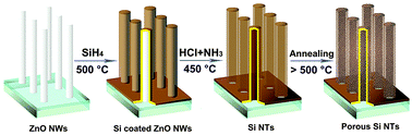 | ||
| Fig. 1 Si nanotube array (Si NTA) fabrication scheme. Si is brought into the system by CVD with silane onto ZnO NWs at 500 °C, with removal of the ZnO core by etching with HCl and NH3. Extent of NT crystallinity is affected by optional annealing. | ||
Nanotube hollow inner diameter is readily manipulated by selection of ZnO NWA growth parameters. We are able to produce ZnO NWA core templates ranging in average width from 30 to 200 nm using a modified version of existing methods for ZnO nanowire formation (Fig. 2a).10,11 Under these conditions, the length of the ZnO nanowires are 5–10 μm with length to diameter ratios (L/D) of ∼10–25, depending on the reactant concentrations in the ZnO growth solution (ESI†).
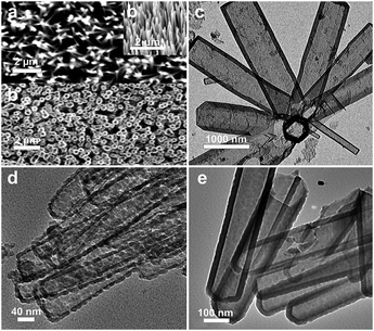 | ||
| Fig. 2 (a) SEM images of a ZnO NWA on a fluorine-doped tin oxide (FTO) substrate. Inset: tilt view (40°); (b) SEM image of an etched Si NTA (scale bars are 2 μm); TEM images of Si NTs of varying shell thickness: (c) relatively thick sidewalls of 100 nm on 500 nm ID hollow structure; scale bar = 1000 nm; (d) thin sidewalls, ∼10 nm, showing porous morphology; scale bar = 40 nm; (e) moderate thickness, ∼25 nm; scale bar = 100 nm. | ||
Chemical vapor deposition (CVD) can be used to add the Si component for subsequent NTA formation. Specifically, silane (150 sccm, 0.5% in He, further diluted in He at 150 sccm) is used to form a Si coating (500 °C) on the surface of ZnO NWs, with the thickness of the Si shell controlled by the duration of the silane exposure (6–10 min), or alternatively, local Si concentration as a function of sample location in the reactor. Visual inspection reveals straightforward differences in sample color as a function of increasing order of thickness, ranging from to light yellow, through brown, and finally to black.
We have investigated different protocols for ZnO NW removal to achieve nanotube formation. In contrast to the high temperature hydrogen reduction process (requiring 50% H2, 600 °C) reported earlier7 or HCl solution-based routes, we find optimal nanotube formation with the novel use of NH4Cl as a precursor for the generation of HCl and NH3 gas phase etchant as low as 450 °C under He carrier gas (100 sccm). Fig. 2b shows the well-aligned morphologies of as-prepared Si NTAs (additional images are also shown in ESI†). In plan view, the hollow core portion of a given structure is readily visible (Fig. 2b). Early experiments provided a striking contrast between the etched and unetched nanowire regions, where cross sectional EDX linescans (and associated TEM image) amplify the loss of the Zn and O upon etching in the structure (ESI†). Thick nanotube shells (ca. 70 nm) typically require multiple etch treatments to fully remove Zn-containing species. Further experiments have shown that no etching reaction occurs at substrate temperatures below 420 °C.
Mechanistically, removal of ZnO likely occurs according to the following reactions:
| ZnO + 2HCl ←→ ZnCl2 + H2O | (1) |
| ZnCl2 + NH3 ←→ Zn(NH2)Cl + HCl | (2) |
While the ZnO core is converted into liquid ZnCl2 (m.p. 292 °C) at 450 °C in reaction (1) and can be removed by an evaporation process, formation of the zinc amide species of reaction (2) and its favorable vapor pressure at the temperatures utilized12 likely facilitates removal of the ZnO NW core.
Control of nanotube shell thickness is a key parameter in terms of manipulation of sidewall structure and associated properties (optical, mechanical). In the experiments described here, sidewall thicknesses ranging from 10 nm to as thick as 100 nm (Fig. 2) have been produced. Significantly, when the sidewall thickness is ∼12 nm or less, the resultant strain in the nanotube produces a unique morphology that appears uniformly porous across a given tube (Fig. 2d). Such voids appear to be in the 5–10 nm range, values associated with a mesoporous classification. Such porosification is presumably driven by a strain-influenced mechanism, whereby Ostwald-type coalescence into islands of Si occurs, with concomitant formation of void spaces in the nanotube. Moving to thicker shell structures (∼25 nm) results in a relatively smooth, continuous surface lacking porous features (Fig. 2e). This is also evident in NTs with even thicker shells, as in the case of 70 nm (ESI†) and 100 nm (Fig. 2c) for two very different inner tube diameters (50 nm, 500 nm).
Such manipulation of nanotube shell thickness, in conjunction with directing the inner diameter size (through control of ZnO NWA template width), provides a widely-tunable overall width of a given nanotube. For example, the overall width of the Si NT structures described above range from 80 nm in (a) to 610 nm in (d). This is a significant expansion of the range provided in earlier studies of Si NTs applied to Li storage and cycling (e.g. 60, 80 and 100 nm).8 The NTAs align in relatively dense films that can be readily fractured into free standing structures for further manipulation (ESI†).
The associated crystallinity of the Si in the as-formed nanotubes is strongly a function of deposition temperature. If the silane decomposition takes place at a temperature of ∼500 °C, only an amorphous Si shell is formed on the surface of ZnO NWs (ESI†). Use of secondary annealing protocols at temperatures of 600 °C (30 min; He atmosphere) and beyond produces readily visible nanocrystalline domains of 〈111〉 orientation (ESI†) present in the nanotube wall.
In an observation of significance to therapeutic applications such as drug delivery and tissue engineering, these Si NTs are observed to dissolve in water (at room temperature) as a function of shell thickness and annealing temperature (Fig. 3; evaluated by molybdate-based spectrophotometric-based methods).13 For example, 23% of Si NTs with a 20 nm shell thickness dissolve in a 47 d period, in contrast to ∼5% for the 80 nm thick variant; annealing Si NTs with a 20 nm thick shell drops the percent dissolution to a value of 11% in this same timeframe. Not surprisingly, use of buffered media at physiological temperature (37 °C) accelerates this process; for example, >80% of a porous Si NT (10 nm thick) sample (∼60 μg) will resorb in a 48 h period, and complete dissolution within 72 h (ESI†). This novel dissolution behavior is reminiscent of bioactive nanostructured mesoporous silicon prepared by the anodization of single crystal silicon.14
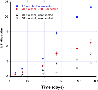 | ||
| Fig. 3 Dissolution of Si NTs for different shell thicknesses (and for the case of 20 nm shell, annealing at 700 °C) as a function of time (in days). | ||
One method to probe the presence of porous sidewalls in such nanotubes is the infiltration of luminescent dyes into the hollow cavity and an evaluation of their photophysics. For this purpose the well studied ruthenium species tris(bipyridyl) ruthenium(II) was selected. Related derivatives of this complex are often employed in dye-sensitized solar cells (DSSCs).15 A typical experiment involves the exposure of a given Si NT film to a dilute ethanolic solution of Ru(bpy)32+, following ethanol rinse and air drying. Such films produce strong visible light that can be viewed via confocal fluorescence microscopy. Steady state emission measurements (λex = 470 nm) reveal the expected 600 nm maximum feature associated with metal to ligand charge transfer (MLCT) in this type of complex.16 The corresponding fluorescence image consists of bright dots consistent with the overall nanotube diameter derived from SEM imaging (Fig. 4). It is also instructive to examine the corresponding lifetimes associated with this emission when present in the nanotube. In thin film form, Ru(bpy)32+ is known to possess two distinct components in its fluorescence decay curves, with τ1 ranging from 80 to 99 ns, and τ2, 329 to 400 ns;17 for films of Ru(bpy)32+ alone ranging from 17 to 200 nm, a direct correlation between increasing film thickness and increasing emission lifetime has been observed.17 Such behavior has been attributed to size-dependent changes in the non-radiative component of the lifetime, knr, in turn mainly associated with effects on the quenching rate for Forster energy transfer (FET).
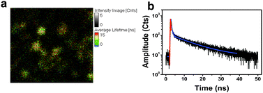 | ||
| Fig. 4 (a) Confocal fluorescence microscopy image of a Si NT array infiltrated with Ru(bpy)32+; λex = 470 nm; field of view = 5 × 5 μm. (b) Corresponding fluorescence decay curve and associated residual analysis of the two exponential fit of the decay curve. The black trace is the collected data, the red trace is the instrument response function calculated by the software, and the blue trace is the exponential decay fit. | ||
For Ru(bpy)32+ loaded into Si NTs, the expected two decay regimes are observed. It is found that that the short lifetime component is significantly reduced to an average value of 10 ns, and the corresponding long lifetime species is lengthened slightly (relative to the above thin film values) to an average of 450 ns. The cause of such an extreme reduction in τ1 is consistent with previous studies of adsorption of Ru(bpy)32+ onto oxide terminated semiconducting surfaces, where electron transfer between the Ru(bpy)32+ and the oxide semiconductor results in a reduction in observed excited state lifetime to 12–20 ns, depending on the substrate.18
In summary, it is clear that the formation of a broad family of nanotube structures is possible with the route demonstrated here. Sensitive control of shell structure has been demonstrated for the case of Si, including a thin-walled variant that dissolves at physiological temperature. Such structures have implications for sensitive drug delivery devices, along with broader electronic applications, at the nanoscale. Proof-of-concept experiments using Ru dye systems reveal strong interactions of the encapsulated complex with the NT surface. A number of additional opportunities for NTs that take advantage of these initial discoveries are currently under investigation.
Financial support of this research by the Robert A. Welch Foundation (Grant P-1212) is gratefully acknowledged.
Notes and references
- M.-H. Park, M. G. Kim, J. Joo, K. Kim, J. Kim, S. Ahn, Y. Cui and J. Cho, Nano Lett., 2009, 9, 3844 CrossRef CAS.
- J. Sha, J. Niu, X. Ma, J. Xu, X. Zhang, Q. Yang and D. Yang, Adv. Mater., 2002, 14, 1219 CrossRef CAS.
- C. Mu, Y. X. Yu, W. Liao, X. S. Zhao, D. S. Xu, X. H. Chen and D. P. Yu, Appl. Phys. Lett., 2005, 87, 113104 CrossRef.
- J. Lan, D. Cheng, D. Cao and W. Wang, J. Phys. Chem. C, 2008, 112, 5598 CAS.
- J. Bai, X. C. Zeng, H. Tanaka and J. Y. Zeng, Proc. Natl. Acad. Sci. U. S. A., 2004, 101, 2664 CrossRef CAS.
- P. Castrucci, M. Scarselli, M. De Crescenzi, M. Diociaiuti, P. S. Chaudhari, C. Balasubramanian, T. M. Bhave and S. V. Bhoraskar, Thin Solid Films, 2006, 508, 226 CrossRef CAS.
- J. Goldberger, R. He, Y. Zhang, S. Lee, H. Yan, H. J. Choi and P. Yang, Nature, 2003, 422, 599 CrossRef CAS.
- T. Song, J. Xia, J. H. Lee, D. H. Lee, M. S. Kwon, J. M. Choi, J. Wu, S. K. Doo, H. Chang, W. I. Park, D. S. Zang, H. Kim, Y. Huang, K. C. Hwang, J. A. Rogers and U. Paik, Nano Lett., 2010, 10, 1710 CrossRef CAS.
- M. Ben-Ishai and F. Patolsky, Nano Lett., 2012, 12, 1121 CrossRef CAS.
- M. Law, L. E. Greene, J. C. Johnson, R. Saykally and P. Yang, Nat. Mater., 2005, 4, 455 CrossRef CAS.
- C. Pacholski, A. Kornowski and H. Weller, Angew. Chem., 2002, 41, 1188 CAS.
- D. Cubicciotti, Inorg. Chem., 1964, 3, 1061 CrossRef CAS.
- S. Kashanian, F. Harding, Y. Irani, S. Klebe, K. Marshall, A. Loni, L. Canham, D. Fan, K. A. Williams, N. H. Voelcker and J. L. Coffer, Acta Biomater., 2010, 6, 3566 CrossRef CAS.
- L. T. Canham, Adv. Mater., 1995, 7, 1033 CrossRef CAS.
- M. Grätzel, J. Photochem. Photobiol., C, 2003, 4, 145 CrossRef.
- E. Klaus and J. Ferguson, in Progress in Inorganic Chemistry, ed. S. J. Lippard, John Wiley & Sons, Hoboken, NJ, 1989, vol. 37, pp. 293–390 Search PubMed.
- K. W. Lee, J. D. Slinker, A. A. Gorodetsky, S. Flores-Torres, H. D. Abruña, P. L. Houston and G. C. Malliaras, Phys. Chem. Chem. Phys., 2003, 5, 2706 RSC.
- T. Kajiwara, K. Hashimoto, T. Kawai and T. Sakata, J. Phys. Chem., 1982, 86, 4516 CrossRef CAS.
Footnote |
| † Electronic supplementary information (ESI) available: Additional details of ZnO NWA and Si NTA fabrication; SEM images of ZnO NWA templates; EDX linescans contrasting a Si NT with an unetched Si/ZnO NW; additional TEM images of Si NT samples with relatively thick sidewalls (70 nm) and a densely-packed Si NTA film; HREM images of an annealed Si NT and porous Si NTs; time dependent dissolution of 10 nm thick Si NTs at 37 °C. See DOI: 10.1039/c3cc41913d |
| This journal is © The Royal Society of Chemistry 2013 |