 Open Access Article
 This Open Access Article is licensed under a Creative Commons Attribution-Non Commercial 3.0 Unported Licence
Visualizing nanoparticle mobility in liquid at atomic resolution†
Madeline J.
Dukes
a,
Benjamin W.
Jacobs
a,
David G.
Morgan
b,
Harshad
Hegde
c and
Deborah F.
Kelly
*c
aApplications Science, Protochips, Inc., Raleigh, NC, USA
bDepartment of Biology, Indiana University at Bloomington, Bloomington, IN 47405, USA
cVirginia Tech Carilion Research Institute, Roanoke, VA 24016, USA. E-mail: debkelly@vt.edu; Fax: +1 540 985 3373; Tel: +1 540 526 2031
First published on 28th February 2013
Abstract
Gold nanorods are widely known for their photothermal properties to treat solid tumors. Our work demonstrates the unrealized capacity to image these reagents in liquid at high resolution using Transmission Electron Microscopy (TEM). Here we perform the first atomic measurements of functionalized nanorods in solution while visualizing their dynamic behaviour with TEM.
The use of microfluidic-based devices has spurred new opportunities to visualize dynamic mobility at the molecular level.1,2 Using these tools scientists have recently watched, for the first time, the growth of nanocrystals into materials and the engulfment of nanoparticles into cells.3–6 These recent technological advancements in conjunction with high-resolution imaging provide a new opportunity to view nanoscale processes as they occur in solution.
A new mode of therapeutic intervention in cancer research employs the use of rod-shaped gold nanoparticles, appropriately termed “nanorods”. Nanorods injected into the circulation can be engineered to target, infiltrate and accumulate in solid tumors.7,8 Upon applying infrared radiation at the tumor site, the high photothermal conversion rate of the nanorods increase the temperature of the surrounding region to kill off cancerous cells.9,10 Although this application for the therapeutic use of nanorods is gaining popularity, the molecular behavior of these nanoparticles has never been observed. Here we present the first high-resolution view of how polyvinyl pyridine (PVP)-encapsulated gold nanorods migrate in liquid using in situ molecular microscopy. In doing so, we also introduce a novel system to view short-range diffusion properties of nanogold-based therapeutic reagents in a native environment.
In our present work, we employ a microfluidic imaging chamber composed of silicon nitride E-chips (Protochips, Inc.) containing 50 nm thick transparent windows. This imaging chamber is assembled within the tip of a Poseidon in situ specimen holder (Protochips, Inc.) that is completely isolated from the vacuum system when inserted into a transmission electron microscope (TEM). This allowed us to image the therapeutic nanorods fully submerged in liquid.
Prior to use, E-chips were rinsed in 150 ml of acetone for approximately 2 minutes followed by a second rinse in 150 ml of methanol and dried under a laminar air-flow. The E-chips were then glow-discharged for 90 seconds using a Pelco Easiglow (Ted Pella, Inc.) to improve wettability of the surface prior to assembling the microchamber. Gold nanorods encapsulated in polyvinyl pyridine (PVP) were purchased from Nanopartz Inc. and diluted in Milli-Q water to a final concentration of 0.17 mg ml−1. Aliquots (1 μl) of the diluted PVP-coated nanorods in Milli-Q water were dispensed onto an E-chip that contained an integrated 150 nm spacer, prepositioned in the tip of the specimen holder. A second, flat, chip was placed on top of the spacer E-chip containing the sample (Fig. 1a). The entire assembly was then sandwiched together to form a sealed enclosure, mechanically held in place by 3 brass screws within the holder. Following assembly, the tip of the holder was pumped to 10−6 Torr using a Gatan 655 dry pumping station (Gatan, Inc.) before placing the holder inside the TEM.
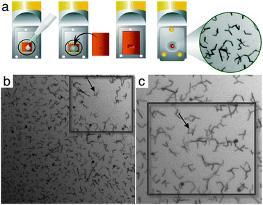 | ||
| Fig. 1 In situ TEM of gold nanorods. (a) Nanorods in solution were added to silicon nitride chips with 150 nm spacers and placed at the tip of a Poseidon specimen holder. A second chip was placed on top to form a sealed liquid chamber that fits into a TEM stage. (b) Nanorods were displaced (black square region) by the incident electron beam creating an empty region that became occupied by diffusing nanorods within 5 seconds (c). Black arrows denote a point of reference between panels and the width of the boxes in (b) and (c) are 1 μm. | ||
The gold nanorods (∼50 nm × 10 nm in size) contained within the tip of the in situ specimen holder were examined by high-resolution electron microscopy. The holder was loaded into a FEI Tecnai Spirit BioTwin TEM equipped with a LaB6 filament and operating at 120 kV. Images of gold nanorods in solution were recorded under low-dose conditions (1–3 electrons per Å2) using a FEI Eagle 2k HS CCD camera having a pixel size of 30 μm at a nominal magnification of 23![[thin space (1/6-em)]](https://www.rsc.org/images/entities/char_2009.gif) 000×. Upon illuminating the specimen with the electron beam, the nanorods initially diffused (Fig. 1b) then quickly returned to fill the same liquid region (Fig. 1c) within approximately 5–10 seconds. The same region is shown in Fig. 1b and c at the initial point of illumination and after particle diffusion. The black arrows in Fig. 1b and c indicate the same cluster of nanorods, serving as a point of reference between panels.
000×. Upon illuminating the specimen with the electron beam, the nanorods initially diffused (Fig. 1b) then quickly returned to fill the same liquid region (Fig. 1c) within approximately 5–10 seconds. The same region is shown in Fig. 1b and c at the initial point of illumination and after particle diffusion. The black arrows in Fig. 1b and c indicate the same cluster of nanorods, serving as a point of reference between panels.
We recorded live footage of the dynamic gold nanorods by outputting raw images from the CCD camera to a computer monitor connected to the TEM using the Tecnai Image Analysis software package (FEI Company). Images were recorded in preview mode with 2×-binning and an integration time of 0.25 seconds. A 0.25 second exposure yielded a total dosage of 0.5 electrons per Å2 per frame (i.e., ∼2 electrons per Å2 × 0.25 s for each frame). Output from the monitor was recorded using a Samsung Galaxy S3 device (Samsung Electronics Company) in 1080p high-definition mode. Footage from each imaging session was imported into iMovie '11 (Apple Inc.) for editing and exported in .mov format. The final version of the movie was accelerated in playback mode to equate to real-time events in the TEM (ESI†).
We could visualize the dynamic behaviour of the gold nanorods in solution throughout the time-course of the imaging experiments. To ensure the chamber remained fully hydrated during the course of our experiments, we recorded representative images of bubble formation in the liquid chamber at the beginning and end of each session (Fig. S1, ESI†). We recorded live footage of the nanorods, during a 16-second time interval (Movie S1, ESI†). This revealed individual nanorods being swept up in migrating liquid fronts that we refer to as “nanoscale tidal waves”. Snapshots that show the progression through the frame sequence indicated micron-scaled movements of the rods in liquid as the waves occurred (Fig. 2). Within the frames, black arrows (Fig. 2, panels 1–4) provide a point of reference during the initial wavefront that brings into view an additional landmark particle, red arrows (Fig. 2, panel 3–6). After the first wave exited, a second wave travelled through the imaging area that concentrated the nanorods into a central location as the liquid recessed. The electron dose accumulation during the course of Movie S1 (ESI†) was ∼32 electrons per Å2.
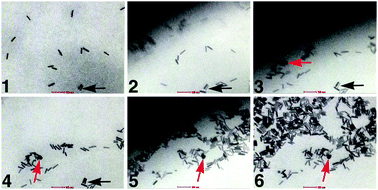 | ||
| Fig. 2 Selected individual frames from Movie S1 (ESI†) indicate the micron-scaled movements of gold rods. Nanoscale tidal waves are the dark fronts emerging from top left corner in panels 2, 3 and 5. These waves pass through the imaging plane and concentrate the rods upon recession. Black arrows (panels 1–4) and red arrows (panels 3–6) provide reference landmarks in the series of images. Scale bar is 100 nm. | ||
Similar wavefront dynamics induced by the electron beam have been described in nanodroplets using in situTEM.11 Likely explanations for this type of physical motion include, beam-induced movement, charging effects and heat accumulation in the liquid cell due to hydrolysis of water molecules or due to the heat capacity of the gold rods themselves. We anticipate these molecular wavefronts may also serve to concentrate gold nanorods injected into tumor microenvironments and contribute to the collective therapeutic process achieved during clinical intervention. We are currently working to test this hypothesis.
To determine the spatial resolution of the PVP-coated gold nanorods contained in the liquid chamber, we used a JEOL 3200FS TEM, equipped with a field emission gun and in-column energy filter operating at 300 kV. Gold nanorods were again loaded into an in situ specimen holder designed for the JEOL instrument. High-resolution images (Fig. 3a) and electron diffraction patterns (Fig. 3b) were recorded using a Gatan UltraScan 4000 CCD camera having a pixel size of 15 μm at a nominal magnification of 100000×. Features of the gold lattice at atomic resolution (∼2 Å spacing) were visible in the recorded images (Fig. 3a). Electron diffraction patterns were recorded in diffraction mode directly onto the CCD camera. Likewise, the gold lattice spacing was clearly visible in the diffraction patterns and revealed information beyond the 2,0,0 lattice plane (Fig. 3b). This corresponds to a spatial resolution of 2.04 Å.
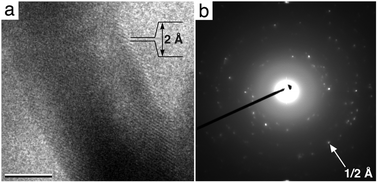 | ||
| Fig. 3 EM image (a) and electron diffraction pattern (b) of gold nanorods in liquid indicate the presence of high-resolution features. The gold lattice spacing of ∼2 Å can be identified in the image. This corresponds to the 2,0,0 plane shown in the electron diffraction pattern (white arrow). Scale bar, 7 nm. | ||
Other recent studies have elegantly used two support films composed of graphene or silicon nitride to form fluidic chambers and to image materials in liquid.4,12,13 However, to our knowledge atomic resolution in liquid, at the level of 2 Å, has not yet been achieved in recorded TEM images or diffraction patterns using other systems. Therefore, our work demonstrates a unique means to observe dynamic reactions at high-resolution using TEM. We are currently testing the resolution of the microfluidic system with other therapeutic reagents and materials.
Collectively, our work provides one of the first demonstrations of atomic imaging in liquid cells composed of silicon nitride microchips using TEM. We also provide an initial glimpse of how biomedical reagents behave in native liquid while bombarded with energy from an external source within a specified time course. Our model system may, therefore, provide a means to better understand molecular events that occur during thermal ablation. We are currently pursuing this clinically relevant area of investigation. Overall, our presented work brings us a step closer to viewing live therapeutic mechanisms of action with a remarkable new level of resolution.
Notes and references
- H. Zheng, S. A. Claridge, A. M. Minor, A. P. Alivisatos and U. Dahmen, Nano Lett., 2009, 6, 2460–2465 CrossRef.
- E. A. Ring and N. de Jonge, Micron, 2012, 43, 1078–1084 CrossRef CAS.
- H. Zheng, R. K. Smith, Y. W. Jun, C. Kisielowski, U. Dahmen and A. P. Alivisatos, Science, 2009, 324, 1309–1312 CrossRef CAS.
- J. M. Yuk, J. Park, P. Ercius, K. Kim, D. J. Hellebusch, M. F. Crommie, J. Y. Lee, A. Zettl and A. P. Alivisatos, Science, 2012, 336, 61–64 CrossRef CAS.
- H. H. Bau and J. M. Grogan, J. Microeletromech. Syst., 2010, 19, 885–894 CrossRef.
- D. B. Peckys and N. de Jonge, Nano Lett., 2011, 11, 1733–1738 CrossRef CAS.
- X. Huang, I. H. El-Sayed, W. Qian and M. A. El-Sayed, J. Am. Chem. Soc., 2006, 128, 2115–2120 CrossRef CAS.
- E. B. Dickerson, E. C. Dreaden, X. Huang, I. H. El-Sayed, H. Chu, S. Pushpanketh, J. F. McDonald and M. A. El-Sayed, Cancer Lett., 2008, 269, 57–66 CrossRef CAS.
- P. K. Jain, X. Huang, I. H. El-Sayed and M. A. El-Sayed, Acc. Chem. Res., 2008, 41, 1578–1586 CrossRef CAS.
- E. C. Dreaden and M. A. El-Sayed, Acc. Chem. Res., 2012, 45, 1854–1865 CrossRef CAS.
- U. M. Mirsaidov, H. Zheng, D. Bhattacharya, Y. Casasna and P. Matsudaria, Proc. Natl. Acad. Sci. U. S. A., 2012, 109, 7187–7190 CrossRef CAS.
- J. E. Evans, K. L. Jungjohann, N. D. Browning and I. Arslan, Nano Lett., 2011, 11, 2809–2813 CrossRef CAS.
- D. Li, M. H. Nielsen, J. R. I. Lee, C. Frandsen, J. F. Banfield and J. J. De Yoreo, Science, 2012, 25, 1014–1018 CrossRef.
Footnote |
| † Electronic supplementary information (ESI) available: Images of bubble formation in liquid cells and live footage of gold nanorods migrating in solution are available as supplemental materials. See DOI: 10.1039/c3cc41136b |
| This journal is © The Royal Society of Chemistry 2013 |