 Open Access Article
Polymer dual ring resonators for label-free optical biosensing using microfluidics†‡
Muhammad H. M.
Salleh
ab,
Andrew
Glidle
b,
Marc
Sorel
c,
Julien
Reboud
b and
Jonathan M.
Cooper
*b
aDepartment of CTS, Kulliyyah of Science, International Islamic University Malaysia, 25200 Kuantan, Pahang, Malaysia
bDivision of Biomedical Engineering, School of Engineering, University of Glasgow, Oakfield Avenue, Glasgow, G12 8LT, UK. E-mail: jon.cooper@glagsow.ac.uk; Fax: +44 (0)141-330 4907; Tel: +44 (0)141-330 5231
cElectronic and Nanoscale Engineering, School of Engineering, University of Glasgow, Oakfield Avenue, Glasgow, G12 8LT, UK
First published on 17th January 2013
Abstract
We demonstrate a polymer resonator microfluidic biosensor that overcomes the complex manufacturing procedures required to fabricate traditional devices. In this new format, we show that a gapless light coupling photonic configuration, fabricated in SU8 polymer, can achieve high sensitivity, label-free chemical sensing in solution and high sensitivity biological sensing, at visible wavelengths.
Label-free sensors within optofluidic systems have emerged as increasingly important tools in biochemical analysis,1 due to their ability to probe the direct interaction between light and the analyte of interest. Microring resonators in particular have been easily integrated within microfluidic systems.2
In this work, we now demonstrate a new variant on the microring resonator, which we have named the dual disk resonator (DDR). The configuration is much easier to fabricate than the micro-ring resonator as it exploits a ‘gap-less’ design, with significantly reduced tolerances in the micro- and nanofabrication processing steps. We first validated the device using a chemical assay, demonstrating the measurement of sucrose concentration in solution (as a function of the local change in refractive index). Subsequently, we showed that the sensor can be readily used to evaluate the dynamics of antibody interactions on surfaces, exploring the assembly (and disassembly) of immuno-constructs using avidin–biotin based immobilisations.
Our work builds upon the well-established understanding of planar waveguide sensor technology, which exploits the interaction between an evanescent field on a surface and analytes present in close proximity to the surface, within the surrounding media. In the case of microring resonators, the extreme sensitivities of such devices (down to single molecule in high Q cavities3) is underpinned by the long lifetime of photons within the resonant cavity, thus increasing the interaction between the light and the analytes. In addition, microring resonators enable such analytical enhancement within a reduced footprint, making their integration within microfluidic devices simpler.
A common fabrication route for microring resonators has involved silicon-based materials for the core waveguide, such as silicon nitride,4 silicon oxide,5 silicon-on-insulator (SOI),6 or Hydex glass.7 These materials are well adapted for use within the communication bandwidth (>1300 nm). The close confinement of the light inside the microring cavity of such devices limits their application to biosensing, where the evanescent field on the top surface of the waveguide has to interact with analytes bound to the surface.
Here, instead we used SU8 (MicroChem Corp.), commonly employed as a resist in photolithography, or as the material for channel walls in microfluidic chips,8 as the material of choice.9 Although other polymers have been used in microring resonators, such as polymethyl-methacrylate (PMMA)10 and polystyrene (PS),11,12 SU8 provides us with a highly processable material. In contrast to many polymers and inorganic materials, the ability to directly pattern SU8 in a single lithographic step makes it attractive (silicon-based materials would require several steps of fabrication, involving reactive ion etching (RIE) and mask layer deposition, rendering manufacturing relatively complex).
Conventional microring resonator structures require a narrow gap between the straight input waveguide and the resonator structure, well below 1 μm width,6,9 so as to enable the efficient coupling of the light (Fig. 1a). This gap can be fabricated by using advanced lithography, but remains a demanding task, especially within a polymer. When using visible wavelengths of light within a biosensor, the gap between the ring resonator and the input waveguide lies below 100 nm (the evanescent tail being around 60 nm).
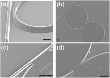 | ||
| Fig. 1 (a) Illustration of a gap, used for evanescent coupling of the light between the waveguide and the traditional resonator configuration. Here we demonstrate a gapless approach (b–d). The sensor system is shown as a gapless dual disk resonator (see Fig. S1 in ESI,‡ for schematic). SEMs of the DDR (40 and 42 μm in diameter) made in SU8 on silicon (see Fig. S2 in ESI‡). (b and c) Close ups on the gapless coupling between the different photonic structures. Scale bars are 5 μm. | ||
Instead, we introduce here the concept of a gapless resonator architecture, where the input light is coupled into the resonator directly (non-evanescently) (Fig. 1). Recently, a gapless strategy for resonator coupling has been modelled13 and applied to delay lines in the field of communication.14 We demonstrate its implementation in biosensing for the first time, enabling simple fabrication of polymer-based devices. Fig. 1(b) shows the fabricated DDR in SU8, while close-ups in Fig. 1(c and d) show the gapless coupling between the structures. The detailed fabrication procedure is described in ESI‡ (supplementary methods and Fig. S2). The microfluidic channel was fabricated using standard soft lithography. SU8 photoresist was patterned with photolithography, to make a master on a silicon wafer, functionalised with a hydrophobic perfluorosilane. PDMS (1/10 w/w ratio of monomer) was poured, degassed and cured (70 °C for 2 h), before being peeled off of the Si master. The channel was then plasma-bonded (O2) to the SU8 DDR chip.
The device was then aligned with the measurement system (Fig. 2 and Fig. S3 in ESI‡) using a HeNe laser (Melles Griot, 5 mW). After the alignment step, the coupling fibre was shifted from the HeNe laser to visible light (100 W, 12 V, Osram). The spectral output from the opposite side of the input waveguide was collimated into a 20× objective lens that projected the signal onto the fibre optics collector. The output signal was propagated onto a spectrum analyzer (500M, Jobin Yvon Horiba) and captured by a charged-coupled device (CCD) (Andor, DU420-BR-DD) camera.
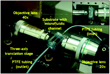 | ||
| Fig. 2 Microfluidic system. The platform comprises a PDMS microfluidic channel delivering reagents and samples to the gapless dual disk resonator (see Fig. S3 in ESI‡). The light probing the sample is introduced via an optical fibre coupled to a 40× microscope lens. It is coupled into the resonators via a waveguide (Fig. 1). The light exiting the sensor is coupled to a 20× objective to an optical fibre, to be analysed by a spectrometer. | ||
The simplest design, as a single disk resonator, was difficult to implement as, given the practical determination of the resonance wavelength (approximately 1.48 nm for the free spectral range (FSR)), the resonance wavelength was hard to distinguish from other peaks. Consequently, we implemented a cascaded double resonator configuration, which has the potential to increase the FSR using the Vernier effect15 (the resonances of the first resonator are enhanced only when they overlap with resonances in the second resonator, while other resonances are suppressed). With these wider FSR values, the resonance shifts become easier to distinguish and observe.
We first characterised the optical sensitivity of the fabricated device using sucrose dilutions to vary the refractive index (RI) of the sample above the waveguide. Fig. 3(a) illustrates the shift observed for different sucrose concentrations, while Fig. 3(b) quantifies the calibration of the RI values for concentrations up to 50% (w/w) sucrose, using an Abbe refractometer. Using the resonance at ∼759 nm as the signal, we then calibrated our dual disk resonator, as shown in Fig. 3(c). We observed a maximum shift of 0.609 nm for a change in RI of 0.048 (12.7 nm per RIU).
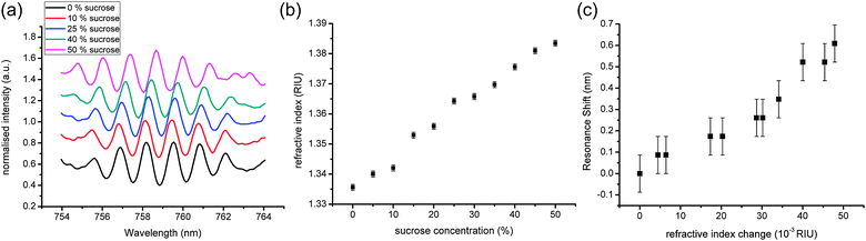 | ||
| Fig. 3 Characterisation of the DDR system with sucrose: (a) representative spectra for different concentrations of sucrose. As the concentration increases, the spectra can be seen shifting to the right; (b) refractive index of different sucrose solutions (measurement error given by the refractometer); (c) resonance shift for different sucrose solutions, as a function of the refractive index. Errors are measurement errors from the spectrometer. | ||
In order to demonstrate the applicability of the device in biosensing, we demonstrated the dynamics of the construction of a model immunoassay, based upon the application of avidin–biotin technology. The microfluidic chip was connected to a syringe pump (Harvard Apparatus) to deliver appropriate reagents sequentially, while the signal from the spectrophotometer was recorded in real-time. Fig. 4(a) shows the spectra (averaged over 3 s) at intervals of 50 s. As the reagents are flown through the chip, the spectrum shifts to higher wavelengths.
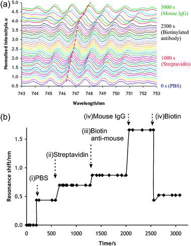 | ||
| Fig. 4 Real-time label-free detection of antibody–antigen binding. The samples were flown within the chip at 1 μl min−1. (a) Full series of recorded resonance spectrum wavelength. Each colour represents 50 s intervals. The dashed (red) line shows the displacement of the monitored resonance peak. (b) Resonance shift over time. Arrows indicate the onset of solution change. (i) PBS media; (ii) streptavidin solution; (iii) biotinylated anti-Mouse IgG; (iv) mouse IgG antigen; (v) concentrated d-biotin solution. | ||
Fig. 4(b) quantifies the wavelength shift as a function of time. Phosphate buffer was first introduced onto a sensor, onto which NHS–biotin (Sigma) had been immobilised via an aminopropyltriethoxysilane (APTES, see Methods in ESI‡).
The introduction of fluid results in a large resonance shift of approximately 0.436 nm. The flow was switched to allow the introduction of streptavidin (VectorLabs, 0.03 mg ml−1) at t = 580 s, which led to a shift of 0.261 nm after 80 s. A biotinylated anti-mouse antibody (Dako, 0.03 mg ml−1), was flowed over the sensor from t = 1300 s until t = 2000 s. The biotin was able to bind to the streptavidin sites, which led to a shift by 0.174 nm during that period. The capability of the device to study the specific interaction of an antigenic reaction was probed by introducing a mouse IgG (Sigma 0.03 mg ml−1). Its specific binding to the anti-mouse species present on the surface was captured by a shift in the resonance wavelength (0.790 nm).
In order to validate whether the observed resonance shifts were a consequence of biotin–streptavidin binding, a concentrated biotin solution (Sigma 10 mg ml−1) was injected into the device (t = 2550 s). The solution-based biotin competes with the assembled biotin molecules, disassembling the complex. This caused the resonance shift to sharply decrease to the level observed before the introduction of streptavidin (0.435 nm), before stabilising at slightly higher values (0.552 nm) perhaps due to some non-specific binding of streptavidin on the sensor.
Here we have demonstrated a dual disk ring resonator integrated within a microfluidic device, with the potential to offer simple fabrication methodologies for optical biosensing. By implementing a gapless architecture, where the waveguides are directly coupled to each other, without the sub-micron gap usually required, we enabled the fabrication of the device in SU8 polymer using a single lithographic step. We validated the device by performing a model antibody–antigen reaction and monitoring it in real-time. In the future, the sensitivity of the device could be greatly improved by coupling more disks in cascade structures.16 Its implementation as a real-time sensor also opens the possibility of studying reaction kinetics, in a similar way as surface plasmon resonance devices.
We acknowledge funding from the Ministry of Higher Education Malaysia (MOHE, SLAB scholarship), the International Islamic University Malaysia (IIUM), and Intilogic Enterprise.
Notes and references
- S. Szunerits and R. Boukherroub, Chem. Commun., 2012, 48, 8999 RSC.
- C. A. Barrios, Anal. Bioanal. Chem., 2012, 403, 1467–1475 CrossRef CAS.
- A. M. Armani, R. P. Kulkarni, S. E. Fraser, R. C. Flagan and K. J. Vahala, Science, 2007, 317, 783–787 CrossRef CAS.
- A. Gondarenko, J. S. Levy and M. Lipson, Opt. Express, 2009, 17, 11366–11370 CrossRef CAS.
- A. Ksendzov and Y. Lin, Opt. Lett., 2005, 30, 3344–3346 CrossRef CAS.
- D.-X. Xu, M. Vachon, A. Densmore, R. Ma, A. Delâge, S. Janz, J. Lapointe, Y. Li, G. Lopinski, D. Zhang, Q. Y. Liu, P. Cheben and J. H. Schmid, Opt. Lett., 2010, 35, 2771–2773 CrossRef CAS.
- A. Ramachandran, S. Wang, J. Clarke, S. J. Ja, D. Goad, L. Wald, E. M. Flood, E. Knobbe, J. V. Hryniewicz, S. T. Chu, D. Gill, W. Chen, O. King and B. E. Little, Biosen. Bioelectron., 2008, 23, 939–944 CrossRef CAS.
- T. Sikanen, S. Tuomikoski, R. A. Ketola, R. Kostiainen, S. Franssila and T. Kotiaho, Lab Chip, 2005, 5, 888–896 RSC.
- U. Levy, K. Campbell, A. Groisman, S. Mookherjea and Y. Fainman, Appl. Phys. Lett., 2006, 88, 111107 CrossRef.
- H. Ma, A. k.-Y. Jen and L. r. Dalton, Adv. Mater., 2002, 14, 1339–1365 CrossRef CAS.
- C.-Y. Chao and L. J. Guo, Appl. Phys. Lett., 2003, 83, 1527–1529 CrossRef CAS.
- R. Horvath, K. Cottier, H. C. Pedersen and J. J. Ramsden, Biosens. Bioelectron., 2008, 24, 799–804 CrossRef CAS.
- L. Shang, A. Wen, B. Li and T. Wang, J. Opt., 2011, 13, 015503 CrossRef.
- X. Luo and A. W. Poon, Opt. Express, 2009, 17, 23617–23628 CrossRef CAS.
- G. Griffel, IEEE Photonics Technol. Lett., 2000, 12, 1642–1644 CrossRef.
- F. Xia, L. Sekaric and Y. Vlasov, Nat. Photonics, 2007, 1, 65–71 CrossRef CAS.
Footnotes |
| † This article is part of the ChemComm 'Microfluidics' web themed issue. |
| ‡ Electronic supplementary information (ESI) available: Materials and methods and additional results. See DOI: 10.1039/c3cc38228a |
| This journal is © The Royal Society of Chemistry 2013 |