 Open Access Article
 This Open Access Article is licensed under a
 Creative Commons Attribution 3.0 Unported Licence
Integrated label-free silicon nanowire sensor arrays for (bio)chemical analysis†
Arpita
De
,
Jan
van Nieuwkasteele
,
Edwin T.
Carlen
* and
Albert
van den Berg
BIOS/Lab on a Chip Group, MESA+ Institute for Nanotechnology, University of Twente, Postbus 217, 7500 AE Enschede, The Netherlands. E-mail: e.t.carlen@utwente.nl; Fax: +31 (0)53 489 3595; Tel: +31 (0)53 489 5399
First published on 28th March 2013
Abstract
We present a label-free (bio)chemical analysis platform that uses all-electrical silicon nanowire sensor arrays integrated with a small volume microfluidic flow-cell for real-time (bio)chemical analysis and detection. The integrated sensing platform contains an automated multi-sample injection system that eliminates erroneous sensor responses from sample switching due to flow rate fluctuations and provides precise sample volumes down to 10 nl. Biochemical sensing is demonstrated with real-time 15-mer DNA–PNA (peptide nucleic acid) duplex hybridization measurements from different sample concentrations in a low ionic strength, and the equilibrium dissociation constant KD ≈ 140 nM has been extracted from the experimental data using the first order Langmuir binding model. Chemical sensing is demonstrated with pH measurements from different injected samples in flow that have sensitivities consistent with the gate-oxide materials. A differential sensor measurement configuration results in a 30× reduction in sensor drift. The integrated label-free analysis platform is suitable for a wide range of small volume chemical and biochemical analyses.
Introduction
Miniaturized analytical assays for the measurement of biomolecular interactions at very low sample concentrations and volumes are becoming increasingly important for applications requiring high-throughput biomolecular analyses, such as genomics screening, protein assays for basic molecular biology research, pharmaceutical drug screening, and disease diagnostics.1 The most common method for biomolecular detection uses a reporter label, such as a fluorophore or radioisotope, chemically attached to the target analyte that indicates binding to a receptor molecule by measuring the emission signal of the reporter label. Currently, fluorescence-based detection of target–receptor biomolecular binding is the most commonly used method, which is well established with many commercially available high quantum yield fluorophores and highly sensitive detectors, however, the labeled approach suffers from the need to conjugate the label to the target and possible alterations in target–receptor interactions caused by conformational changes or steric hindrance induced by the label.2There have been considerable efforts over the last two decades to develop label-free measurement techniques that can directly record biomolecular complex binding events without significantly altering the native biomolecular conformation. Isothermal titration calorimetry and differential scanning calorimetry are truly label-free methods that can measure the thermodynamic binding properties in the native biomolecular environment.3 Although the calorimetric methods are extremely powerful, they are currently limited to large sample volumes and concentrations. Alternatively, the receptor molecule can be tethered directly to a sensor surface that can measure in real-time the change of surface properties as the target analyte binds to the receptors. Currently, many different surface-based label-free sensor systems are available that use different detection phenomena, such as surface plasmon resonance, optical interferometry, optical gratings, quartz crystal microbalance, and surface acoustic waves.4 Surface plasmon resonance sensors5 and surface plasmon resonance imaging sensors6 are well-established label-free techniques, but they require sophisticated optical instrumentation for signal readout and have limited sensitivity, especially for small molecular weight molecules. All-electrical sensor configurations are promising, such as the direct readout of biomolecular binding using electrochemical labels,7 or semiconductor transistors that measure the intrinsic electronic biomolecular charge on the gate-oxide using a field-effect to modulate the device conductance.8,9
There has been a steady increase in reports on ultrasensitive field-effect biosensors over the past several years based on semiconductor nanowires.10 One-dimensional electrical semiconductor nanowire sensors are particularly important due to their potential for large-scale, high-density integration and interfacing to conventional electronic systems, and hence are attractive for low cost portable sensing systems. Silicon nanowire (Si-NW) field-effect transistor (FET) biosensors have been reported extensively for highly sensitive, label-free, and real-time detection of biomolecular binding of DNA and proteins.11,12 The high detection sensitivity of Si-NW biosensors has been attributed to their large surface-to-volume ratio and the three-dimensional multi-gate structure; both contribute to the improved sensitivity compared to conventional planar devices. However, device and technology developments have been limited to a small number of research laboratories typically relying on expensive nanolithography, specialized equipment and processes, or difficulties associated with alignment and electrical contacting into large sensor arrays. We recently reported a new scalable Si-NW sensor technology based on conventional microfabrication that does not require expensive nanolithography and can be implemented into large sensing arrays.13 The main advantage of our technology is that dense Si-NW sensor arrays, with precisely controlled dimensions and atomically smooth surfaces, can be manufactured in any conventional clean room, and can be integrated with small volume microfluidic channels with conventional bonding and clamping techniques.
In this article, we present an integrated label-free analysis platform that is suitable for a wide range of small volume real-time chemical and biochemical analyses. The integrated microfluidic label-free analysis platform uses an analysis cartridge consisting of Si-NW sensor arrays, for (bio)chemical detection and analysis, integrated with a small volume microfluidic flow-cell. The low power Si-NW (bio)chemical sensor cartridge has been developed for an automated molecular diagnostic system that is integrated in an ingestible pill. Sample delivery in the integrated analytical instrument is performed with an automated multi-sample injection system that eliminates erroneous sensor responses from sample switching due to flow rate fluctuations and provides precise sample volumes. The sample transport to the sensor surface is controlled to ensure that reaction-limited binding models can be used to estimate the biomolecular affinity. We describe the components of the integrated measurement system and its use for meaningful data acquisition for real-time biosensing applications. We demonstrate the efficacy of the integrated system for biochemical sensing with real-time DNA–PNA (peptide nucleic acid) duplex hybridization measurements together with an estimation of the binding affinity. Chemical sensing is performed by measuring sample pH under flow conditions of sequentially injected sample buffers.
Experimental
Materials
Si-NW sensors were fabricated from silicon-on-insulator (SOI) wafers (G4P-005-02, Soitec). Triangular Si-NWs have been fabricated using the previously reported method developed by our group that uses conventional microlithography, wet anisotropic etching (5% tetramethyl-ammonium-hydroxide) and size reduction, oxidation, and dry etching.13 The microfluidic chip is manufactured from poly-dimethylsiloxane (PDMS) cast on a silicon mold using a 10![[thin space (1/6-em)]](https://www.rsc.org/images/entities/char_2009.gif) :1 pre-polymer (Sylgard 184) to curing agent (Dow Corning) mixture. Inlet and outlet holes were formed in the microfluidic flow-cell with a punch tool (ϕ 0.5 mm Unicore, Harris). All hydraulic connections between the regulated pressure source (MFCS-8C, Fluigent), sample reservoir tubes (T341-6TLST 2 mL, Econo Lab), sample injection valve (Cheminert Nanovolume 10-port valve, Valco Instruments Co. Inc.) and microfluidic chip are made with 360 μm outside diameter polyether–ether–ketone (PEEK) tubing (TPK10X, Valco Instruments Co. Inc.). Amine functional groups are conjugated to the gate-oxide sensor surface using a 3-amino-propyl-triethoxy silane (APTES) monolayer. The amine-functionalized surface was activated with a 5 mM sulfo-succinimide-maleimide cyclohexane carboxylate cross-linker (SSMCC, Pierce-Thermo Scientific). A synthetic 15-mer thiolated PNA probe was used for all hybridization experiments with sequence Cys-TGT-ACA-TCA-CAA-CTA-NH2. The complementary (M0) DNA sequence is 5′-TAG-TTG-TGA-TGT-ACA-3′ (Eurogentec). The non-complementary (NC) DNA sequence is 5′-ATC-AAC-ACT-ACA-TGT-3′ (Eurogentec). DNA–PNA duplex hybridization on the gate-oxide of Si-NWs was performed in a 1 mM phosphate buffer with pH 7.4. A fluorophore (Cy5) labeled PNA probe (Eurogentec) was used as a control to confirm conjugation of the PNA probe to the gate-oxide sensor surface.
:1 pre-polymer (Sylgard 184) to curing agent (Dow Corning) mixture. Inlet and outlet holes were formed in the microfluidic flow-cell with a punch tool (ϕ 0.5 mm Unicore, Harris). All hydraulic connections between the regulated pressure source (MFCS-8C, Fluigent), sample reservoir tubes (T341-6TLST 2 mL, Econo Lab), sample injection valve (Cheminert Nanovolume 10-port valve, Valco Instruments Co. Inc.) and microfluidic chip are made with 360 μm outside diameter polyether–ether–ketone (PEEK) tubing (TPK10X, Valco Instruments Co. Inc.). Amine functional groups are conjugated to the gate-oxide sensor surface using a 3-amino-propyl-triethoxy silane (APTES) monolayer. The amine-functionalized surface was activated with a 5 mM sulfo-succinimide-maleimide cyclohexane carboxylate cross-linker (SSMCC, Pierce-Thermo Scientific). A synthetic 15-mer thiolated PNA probe was used for all hybridization experiments with sequence Cys-TGT-ACA-TCA-CAA-CTA-NH2. The complementary (M0) DNA sequence is 5′-TAG-TTG-TGA-TGT-ACA-3′ (Eurogentec). The non-complementary (NC) DNA sequence is 5′-ATC-AAC-ACT-ACA-TGT-3′ (Eurogentec). DNA–PNA duplex hybridization on the gate-oxide of Si-NWs was performed in a 1 mM phosphate buffer with pH 7.4. A fluorophore (Cy5) labeled PNA probe (Eurogentec) was used as a control to confirm conjugation of the PNA probe to the gate-oxide sensor surface.
Methods
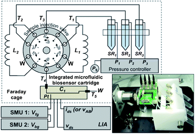 | ||
| Fig. 1 Schematic diagram of the integrated label-free analysis system with automated multi-sample delivery to the microfluidic chip. PEEK tubing is used for all hydraulic connections T1–T5 and sample loops L1 and L2. C1 is the microfluidic flow-cell channel. The pressures P1–P3 control the flow rate in tubes T1–T3, respectively. The dotted enclosure represents the Faraday cage. The electrical biasing and measurement equipment are connected to the Si-NW chip using coaxial cables and a common ground point on the custom-made circuit board. Inset: image of the analysis system. The sample injection valve has two switch positions A and B. | ||
Microfluidic flow-cell. Following surface cleaning of the Si-NW sensors, and subsequent modification with probe biomolecules as required, the Si-NW sensor chip is attached and wire bonded to a custom-made circuit board. The assembled Si-NW sensor chip is then aligned and clamped to the PDMS microfluidic chip, which is simple and non-destructive to the sensor surfaces and probe biomolecules on the sensor surfaces. Fig. 2a shows a schematic diagram of the integrated microfluidic biosensor analysis cartridge. The inlet and outlet holes of the PDMS microfluidic channel are connected to the sample injection valve with PEEK tubing. For experiments presented in this article the PDMS microfluidic channel is 1 cm in length and 360 μm in diameter. A platinum wire (267171, Sigma-Aldrich) pseudo-reference electrode is inserted directly into the microfluidic channel. Fig. 2b shows an example of an integrated microfluidic biosensor cartridge with inlet and outlet holes that are interfaced directly to the PEEK tubing. The analysis cartridge is mounted and wire bonded to a custom-made circuit board.
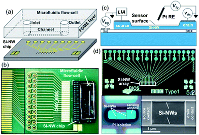 | ||
| Fig. 2 Integrated microfluidic biosensor cartridge consisting of a Si-NW biosensor chip integrated with a microfluidic flow-cell. (a) Schematic of a Si-NW sensor chip and a PDMS microfluidic flow-cell. (b) Optical microscopy image of the implemented integrated microfluidic biosensor cartridge with the Si-NW biosensor chip attached and wire bonded to a custom circuit board, and a bonded microfluidic flow-cell. (c) Length cross-section schematic of a Si-NW biosensor with back-gate Vbg, front-gate Vfg, and drain–source vds bias voltages. Liquid gating of the Si-NW is controlled with a Pt reference electrode (RE) connected to Vfg. A lock-in amplifier (LIA) measures the sensor current. (d) Microscopy images of fabricated Si-NWs. Upper: Si-NW sensor chip (1 cm × 2 cm). Lower left: Si-NW sensor encapsulated with a PI layer and patterned sensing window. Lower right: high-resolution SEM image of a 2-wire Si-NW sensor. | ||
Si-NW sensors. The fabrication technology is capable of producing high-density Si-NW arrays with device diameters down to 10 nm. The Si-NW sensors are boron doped (Na ∼ 1018 cm−3) with heights between 100 nm and 140 nm, measured with atomic force microscopy (AFM). Boron doping was done with conventional ion implantation and N2 anneal at 1000 °C for 30 minutes for dopant drive-in and activation. The aluminium electrical contacts have been annealed at 450 °C for 20 minutes in an H2/N2 forming gas to reduce interface effects and ensure ohmic and low metal-silicon contact resistance. The Si-NW chips were then encapsulated with a 2.5 μm thick polyimide (PI) (annealed at 350 °C for 1 h) electrical isolation layer that has lithographically patterned sensing windows over the Si-NW sensor regions and electrical contact regions. A 15 nm thick silicon dioxide gate-oxide layer was used for pH measurements and a 2 nm thick gate-oxide layer was used for DNA hybridization experiments. Fig. 2c schematically shows the Si-NW length cross-section with all electrical bias voltages and electrical current measurement with a lock-in amplifier (LIA). Fig. 2d shows an example of the Si-NW chip with an array of 2-wire Si-NW sensors (white highlighting) and a patterned sensing window in the PI isolation layer is shown in the lower left image of Fig. 2d. A high-resolution scanning electron microscopy (SEM) image that is representative of Si-NWs fabricated with this technology is shown in the lower right image of Fig. 2d.
pH sensor. The surface potential ψo of the Si-NW gate-oxide is dependent on the pH of the sample solution and is obtained through the titration of the gate-oxide in the presence of a supporting electrolyte. The Si-NW sensor surface is first cleaned with UV ozone, as previously described, and then the Si-NW sensor chip is attached and wire bonded to a custom circuit board and clamp-bonded with the PDMS microfluidic chip. The platinum reference electrode is inserted into the microfluidic flow channel. Prior to solution measurements, a 0.1 M NaCl supporting electrolyte with 0.01 M universal buffer mixture (UBM: 0.01 M citric acid, 0.01 M phosphoric acid, and 0.02 M boric acid) solution at pH 4 was flowed from SR2 (Fig. 1) through the microchannel for 20 minutes to equilibrate the sensor surface.18 The pH 7 and 10 solutions were realized by titrating the starting solution with a 1 M NaOH solution.
DNA hybridization. The surface potential ψo of the Si-NW gate-oxide is dependent on the intrinsic electronic charge of biomolecules, such as DNA hybridized with complementary probes attached near the sensor surface. A sensor response is obtained by measuring the device conductance change, which is dependent on surface potential changes as target biomolecules accumulate on the gate-oxide surface in the presence of an aqueous buffer. Following cleaning of the gate-oxide surfaces with UV ozone, amine functionalized monolayers were silanized to the gate-oxide with APTES in 95% ethanol and 5% deionized water for 1 hour. The surface was then washed with ethanol and followed by a cross-linking heat treatment at 110 °C for 15 minutes (Fig. 3a). The surface is then activated with the SSMCC cross-linker in a 100 mM triethanolamine buffer with pH 7.2 for 1 hour (Fig. 3b). The surface is then incubated in 1 μM thiolated PNA in the same buffer for 12 hours (Fig. 3c). We used a 60 μl volume PDMS incubation well clamped to the Si-NW chip placed in a humidity chamber for all surface chemistry steps. The efficacy of the PNA probe attachment is demonstrated by comparing Fig. 3d and e. A negative control surface without a maleimide functional group was incubated with a PNA-Cy5 conjugate, and following a washing step we ideally expect that the Si-NW sensor regions are black, however, some fluorescence is detected due to non-specific PNA adsorption (Fig. 3d). The bright red regions are due to the silicon nitride layer covering the drain–source contacts. The silicon dioxide layer thickness in the sensor region is approximately 340 nm and quenching of the Cy5 fluorophore by the silicon is not possible in this case. The non-specific adsorption of PNA to glass is well known and we will return to this later in the article. A positive control surface containing an amine functional group following cross-linking activation and incubation with the PNA-Cy5 conjugate shows a uniform red color across the surface and confirms the PNA attachment to the gate-oxide surface (Fig. 3e). Subsequent studies of DNA–PNA hybridized duplexes attached to an oxide surface using radioactive labeling indicate surface densities Nd ∼ 1012 molecules cm−2.
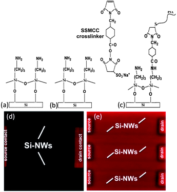 | ||
| Fig. 3 PNA attachment to the Si-NW gate-oxide surface. (a–c) PNA attachment scheme. (d) Negative control incubated with a PNA-Cy5 conjugate. A single Si-NW sensor pair is shown. (e) Positive control incubated with PNA-Cy5. Three Si-NW sensor pairs are shown. | ||
For all measurements presented in this article, the device operation was controlled with dc voltage sources Vfg and Vbg (2400 SMU, Keithley). The platinum wire reference electrode provides the front-gate bias in solution. The Si-NW is driven with an ac (30 Hz) modulation voltage vds and the ac device current is converted to a voltage with a transconductance amplifier (TA) and the magnitude and phase of the signal are measured with a lock-in amplifier (LIA) (SR 830, Stanford Research Systems). For single sensor measurements the internal TA of the LIA is used (Fig. 4a). The LIA uses quadrature synchronous demodulation, with an internal oscillator that is frequency matched to vds, to retrieve the magnitude and phase of ids. We report the magnitude of the measured signal from the LIA, i.e. |ids|. All biasing and measurement instruments are controlled using a custom-made Labview program.
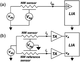 | ||
| Fig. 4 Electrical measurement configurations. (a) Single-device measurement circuit. (b) Differential measurement circuit. | ||
pH and DNA hybridization sensor. Following cleaning of the gate-oxide sensor surface, and subsequent surface modification for biosensing applications, the integrated microfluidic sensor cartridge is placed in the integrated system. PEEK tubing attached to the inlet port was connected directly to the pressurized sample reservoir tubes (SR1, SR2 and SR3), which are filled with 2 ml of sample buffers with varying pH or DNA concentrations. The buffer solution was pumped through the system. For pH sensor experiments, the front-gate response curve Vfg–|ids| was first recorded and analyzed in the initial solution (pH 4). The NW current |ids| was recorded for pH 7 and 10 solutions, injected sequentially from SR2 and SR3, flowing through the microfluidic flow-cell. The measured pH sensitivity Δψo/ΔpH was then calculated using the measured front-gate calibration curve (ref. 20). The hybridization buffer for DNA hybridization experiments is transported from SR1 until the surface was stabilized, i.e. about 20 minutes. The different DNA concentration samples were then injected and the corresponding |ids| was recorded for the duration of the experiment.
Differential measurements. A differential measurement configuration (Fig. 4b) provides the capability to cancel environmental sources of noise and interference, thus yielding measurements that better represent hybridization events compared to single sensor configurations. For differential measurements, two external TA (SIM918, Stanford Research Systems) are used to convert the currents from the reference and sensor devices into voltages vA and vB, respectively. The LIA measurement is then performed in differential mode (vA − vB).
Results and discussion
Integrated Si-NW sensor operation and characterization
Si-NW FET sensors measure surface potential changes Δψo on the sensor surface that originate from changes in the surface charge density Δσo due to changes in surface ions and/or the intrinsic charge of attached biomolecular complexes, as previously described. The surface potential change Δψo is determined from measurements of ΔG from homogeneously doped p-type depletion-mode Si-NWs. We recently reported that the conductance of depletion-mode Si-NWs can be operated in either the depletion or accumulation regions, thus the conductance is G = qμbNaL−1ξ + 2ημaWaL−1Qa, where q is the electronic charge, μb is the dopant concentration dependent bulk hole mobility, Na is the boron impurity dopant concentration in the NW body, L is the device length, ξ is a gating function that is dependent on ψo (see ESI†), μa is the field dependent hole mobility in the accumulated layer, Wa is the total surface area of the accumulated surface and Qa is the electronic charge in the accumulation layer.21 For all measurements presented in this article, the Si-NWs are operated in the depletion region where Qa = 0 since |Vfg| < |Vfb|, where Vfb is the flatband voltage that represents all potential drops across the gate-oxide–silicon interface. It should be noted that the conductance associated with the metal/semiconductor drain and source contact regions has been carefully designed and characterized to have a negligible contribution to the total device conductance (see ESI†). In summary, there are a few important points to highlight regarding the practical operation of Si-NW FET sensors: (i) the application of a dual gate biasing configuration with a reference electrode in the sample buffer ensures optimal and reproducible device behavior; (ii) the sensor surface should be well cleaned (e.g. short duration UV ozone) and the detrimental effects from the fixed oxide charges and surface states at the gate-oxide–silicon interface minimized through thermal annealing; and (iii) the contact resistance of the drain and source contacts should be minimized such that it represents a small fraction of the total quiescent sensor resistance.The Si-NWs were characterized prior to experiments to assess the front-gate Vfg–|ids| and gm–|ids| response curves, where gm = ∂|ids|/∂Vfg (vds constant) is the sensor transconductance. Front-gate biasing affects the depletion region differently compared to back-gate biasing, as previously described, and for biosensor applications, the devices can be biased in the region with highest gm and linear |ids| range while maintaining a low front-gate current ifg < 1 nA.21,22 The back-gate bias Vbg is determined and fixed during the initial calibration. Fig. 5a shows a representative example of a Vfg–|ids| response curve of a Si-NW where the front-gate voltage is scanned with a platinum reference electrode in a low ionic strength buffer (pH 4) and |ids| recorded. The operation region transitions from depletion to accumulation as Vfg is scanned to larger negative voltages. The decrease in gm for Vfg beyond the maximum is due to a decrease in field-dependent effective mobility μa and charge screening. For all experiments, the Si-NW devices are biased with Vfg = −0.6 V and Vbg = −7.5 V, unless specified otherwise.
![Integrated biosensor analysis platform measurements. (a) Si-NW front-gate biasing characteristics in pH 4 buffer solution with a platinum reference electrode. (b) pH measurements with flow speed vs ≈ 0.1 mm s−1. (c) DNA–PNA duplex hybridization detection with [C]3,M0 = 500 nM, [C]2,M0 = 100 nM and [C]1,NC = 100 nM target concentrations and flow speed vs ≈ 0.6 mm s−1. (d) Differential measurement in buffer solution.](/image/article/2013/AN/c3an36586g/c3an36586g-f5.gif) | ||
| Fig. 5 Integrated biosensor analysis platform measurements. (a) Si-NW front-gate biasing characteristics in pH 4 buffer solution with a platinum reference electrode. (b) pH measurements with flow speed vs ≈ 0.1 mm s−1. (c) DNA–PNA duplex hybridization detection with [C]3,M0 = 500 nM, [C]2,M0 = 100 nM and [C]1,NC = 100 nM target concentrations and flow speed vs ≈ 0.6 mm s−1. (d) Differential measurement in buffer solution. | ||
The pH measurements using the integrated microfluidic Si-NW sensor platform were carried out using vds = 100 mV, Vbg = −7.5 V and UV ozone cleaned gate-oxide sensor surfaces. Firstly, a pH 4 buffer solution was transported through the microfluidic flow-cell for 20 minutes to establish a stable baseline signal, and followed by the injection of a buffer solution with pH 7 for 2 minutes and finally the injection of a pH 10 buffer for 3 minutes, all at a flow rate of 0.5 μl min−1, which corresponds to an average flow speed vs ≈ 0.1 mm s−1. For p-type depletion mode Si-NWs, increasing the solution pH results in an increasingly negative surface potential change, which results in a reduced depletion region of the depletion-mode Si-NW devices, and therefore, an increase in |ids|. Fig. 5b shows the pH response of the integrated Si-NW sensor system to different pH sample solutions. From Fig. 5a, the slope of the Vfg–|ids| response curve is Δ|ids|/ΔVfg ≈ −2.6 mV nA−1 (at Vfg = −0.6 V) over the pH experiment range. The right-side ordinate of Fig. 5b shows the estimated surface potential change as the solution is increased from pH 4 to pH 10. Note that the surface potential change is estimated from the initial experimental sample with pH 4. The bare gate-oxide surfaces demonstrate the well-known nonlinearity for low pH values near the point of zero charge (pHpzc ≈ 2), which becomes linear for pH 5 and above.18,21 The measured current shows a sharp increase followed by a gradual increase to the steady state response for an increase in pH from 7 to 10, which is characteristic of the time dependent surface equilibration of the oxide surface. Over the range 7 ≤ pH ≤ 10 the pH sensitivity is Δψo/ΔpH ≈ 48 mV pH−1, which is consistent with measurements in previous experimental results using conventional laboratory sample volumes.21 This measurement demonstrates that the integrated system can provide stable and well-controlled pH sensing with small sample volumes over the time scale of minutes. Other sensing surfaces, such as Al2O3 or Ta2O5, which are well known to provide near Nernstian sensitivity and linear pH responses,21,23 can be easily incorporated into the Si-NW sensing chip.
We present real-time DNA–PNA duplex hybridization measurements of complementary M0 DNA target molecules to PNA probe molecules covalently conjugated to the silicon oxide gate-oxide surface of 2-wire Si-NW sensors (Fig. 3b) in a low ionic strength buffer. The measurements have been performed with sample flow speeds high enough to ensure reaction-limited transport of the target DNA to the sensor surface and we use the first-order Langmuir binding model to assess the equilibrium dissociation constant KD of the DNA–PNA duplex hybridization process. The equilibrium dissociation constant is defined as KD = ka/kd, where ka is the association rate constant that represents the speed of the second-order probe–target interaction and kd is the dissociation rate constant that represents the speed of the first-order breakdown of the probe–target complex. Thermodynamics dictates the target–probe hybridization process and a small KD value indicates a high affinity of the probe for the target, which generally lies in the 10−15M < KD < 10−6 M range.30
From mass action kinetics, the time dependent surface density formation of a single type of probe–target complex on the surface can be monitored in real-time with the response function R(t) = Ro(1 − exp[−(ka[C] + kd)t]), where Ro = (kaRmax[C])/(ka[C] + kd), Rmax is the maximum sensor signal response for a given probe density Np and [C]i is the concentration of the target analyte. The time dependent response function, which is derived by solving a rate equation that includes the association and dissociation of target molecules with surface probe molecules as a function of time, is commonly referred to as the Langmuir equation. The real-time response measured from the Si-NW sensors is drain–source current, thus R(t) ≡ |ids|(t) for fixed biases Vfg, Vbg and vds, and target concentration [C]i for each measurement. Fig. 5c shows measured real-time current responses for injections of M0 DNA with [C]2,M0 = 100 nM and [C]3,M0 = 500 nM concentrations in 1 mM phosphate buffer (λD ≈ 10 nm) to complementary PNA probe molecules conjugated to the gate-oxide surface with a sample flow speed of vs ≈ 0.6 mm s−1. The sensor response to the injection of NC DNA with [C]1,NC = 100 nM is also shown in Fig. 5c, which is the baseline noise from the measurement. The 500 nM concentration M0 DNA produces Δ|ids| ≈ 1 nA and 100 nM M0 DNA produces Δ|ids| ≈ 0.4 nA, as shown in Fig. 5c. The estimated limit of detection is 50 nM, using a 3-sigma cutoff of the measured NC100 nM data noise, for the experimental conditions used in this article and can be reduced, which will be discussed later in this section. The increase in conductance with an increase of negatively charged molecules on the gate-oxide sensor surface of the p-type depletion mode sensor is expected from the sensor characterization (Fig. 5a). We have measured the density of DNA–PNA duplexes formed on oxide surfaces in equilibrium, using a 32P radioactive assay (data not shown), and found that a saturated surface contains about Nd ∼ 1012 duplexes cm−2, which corresponds to a lower limit Δψo ∼ 10 mV (ref. 31) using an oxide charge density σox ≈ 0.2 C m−2 for a buffer with pH 7.21 The estimated surface potential changes correspond to larger conductance changes compared to the measured conductance changes and we are currently working to optimize the PNA probe sensor surface.
The association and dissociation rate constants, ka and kd, are extracted by fitting the measured current responses to the kinetics response function using all of the experimental concentrations. The solid lines in Fig. 5c represent the model fit to the measured data with Rmax ≈ 1 nA, ka ≈ 3 × 10⁴ M−1 s−1 and kd ≈ 4 × 10⁻³ s−1, which gives KD = 140 nM. The Rmax value is consistent with [C]3,M0 > KD, where all PNA binding sites are assumed to be occupied. The extracted KD is much larger than dissociation constants extracted from measurements of the DNA–PNA duplex hybridization.28,29,32 A dissociation constant of KD ≈ 350 nM for a DNA–PNA duplex hybridization at 35 °C has been reported.33 The discrepancy between the measurements can be due to differences in the PNA attachment scheme.29 Extracted KD values of DNA–DNA duplex hybridization measured using Si-NW sensors in a 165 mM ionic strength buffer are similar to our measurements.12
We have found in subsequent studies that PNA molecules non-specifically adsorb to many types of surfaces. Although it is well known that PNA molecules non-specifically adsorb to glass surfaces (Eurogentec), they also adsorb non-specifically to silicon nitride, PDMS and polyimide surfaces with similar attachment densities, and are difficult to remove in most cases (data not shown). The non-specific adsorption of PNA on the polyimide surface is problematic and can negatively affect the estimation of the dissociation rate kd and the limit of detection to target depletion. Following the kinetics and transport analysis that describe the interaction of target analytes with probe molecules on surfaces,34–36 we can further assess the validity of our measurements. From the channel dimensions and sample flow rate, the transport of target DNA to the sensing surface is reaction-limited since the Damkohler number Da ≈ 2 × 10⁻³, thus verifying the use of the single complex formation response function. From Fig. 5c, the time constant τr = (ka[C]i + kd)−1 of the 100 nM response τr ≈ 2 minutes and the 500 nM response has τr ≈ 1 minute, which is much smaller than the time constants measured in previous DNA–PNA duplex formation studies where τr ∼ 10 minutes have been reported.28,29 Fast DNA–PNA and DNA–DNA duplex hybridization times have been reported in other Si-NW sensor studies.12,37 More work is required to understand these differences and to optimize the PNA probe density and minimize the non-specific adsorption of PNA to surfaces that interface with the target DNA.
Conclusions
We have presented an integrated microfluidic label-free analytical platform that can be used for small volume chemical analysis, such as pH or ion sensing, as well as diagnostics for the specific measurement of biomolecules and for the kinetics estimation of biomolecular hybridization. We have integrated a scalable silicon nanowire sensor chip with a microfluidic flow-cell into a simple disposable cartridge format that is mounted into the all-electrical readout instrument. An automated multi-sample injection system was presented that provides fast and reliable sample switching without spurious flow rate fluctuations that can produce erroneous sensor signals. Measurements of pH from different samples have been presented with sensitivities consistent with a silicon dioxide sensor surface. Real-time DNA–PNA duplex hybridization measurements have been presented with different sample concentrations in a low ionic strength buffer, and the equilibrium dissociation constant KD ≈ 140 nM has been extracted from the experimental data using the first order Langmuir binding model. Finally, a differential sensor configuration has been presented and a 30× reduction in sensor drift has been shown. The integrated microfluidic label-free analysis platform with a measurement cartridge based on an electronic Si-NW biosensor array, integrated with a simple microfluidic flow-cell, has been demonstrated by measuring different sample types. The Si-NW (bio)chemical sensor cartridge has been developed for an automated molecular diagnostic system integrated in an ingestible pill, and is a promising platform for low cost (bio)chemical diagnostics and drug screening.Acknowledgements
This work was supported by the Nanopill project funded by a private cancer research foundation in the Netherlands and the Beyond Moore NanoNextNL Program funded by the Government of the Netherlands. The authors thank Johan Bomer for helpful comments on device processing and measurements, Hans de Boer for assistance with the measurement setup and chip holder, the MESA+ Nanolab staff, Mark Smithers for assistance with SEM imaging, and Rico Keim for TEM sample preparation and imaging.Notes and references
- P. Bertone and M. Snyder, FEBS J., 2005, 272, 5400 Search PubMed.
- N. Ramachandran, D. N. Larson, P. R. Stark, E. Hainsworth and J. LaBaer, FEBS J., 2005, 272, 5412 CrossRef CAS.
- W. Gu, Trends in Bio/Pharmaceutical Industry, 2009, 5, 43 Search PubMed.
- J. Comley, Drug Discovery World, 2008, Fall 28 Search PubMed.
- J. Homola, S. S. Yee and G. Gauglitz, Sens. Actuators, B, 1999, 54, 3 CrossRef.
- G. Krishnamoorthy, E. T. Carlen, J. G. Bomer, A. van den Berg and R. B. M. Schasfoort, Lab Chip, 2010, 10, 986 RSC.
- P. M. Levine, P. Gong, R. Levicky and K. L. Shepard, Biosens. Bioelectron., 2009, 24, 1995 CrossRef CAS.
- P. Bergveld, Sens. Actuators, 1981, 1, 17 CrossRef.
- J. Fritz, E. B. Cooper, S. Gaudet, P. K. Sorger and S. R. Manialis, Proc. Natl. Acad. Sci. U. S. A., 2002, 99, 14142 CrossRef CAS.
- E. T. Carlen and A. van den Berg, Lab Chip, 2007, 7, 19 RSC.
- Y. Cui, Q. Q. Wei, H. K. Park and C. M. Lieber, Science, 2001, 293, 1289 CrossRef CAS.
- Y. Bunimovich, Y. S. Shin, W.-S. Yeo, M. Amori, G. Kwong and J. R. Heath, J. Am. Chem. Soc., 2006, 128, 16323 CrossRef CAS.
- S. Chen, J. G. Bomer, W. G. van der Wiel, E. T. Carlen and A. van den Berg, ACS Nano, 2009, 3, 3485 Search PubMed.
- Assuming a PEEK tubing sample loop with a diameter of 25 μm and a length of 2 cm.
- D. R. Kim, C. H. Lee and X. L. Zheng, Nano Lett., 2009, 9, 1984 CrossRef CAS.
- E. H. Snow, A. S. Grove and D. J. Fitzgerald, Proc. IEEE, 1967, 55, 1168 Search PubMed.
- B. E. Deal, J. Electrochem. Soc., 1974, 121, C198 Search PubMed.
- L. Bousse, N. F. de Rooij and P. Bergveld, IEEE Trans. Electron Devices, 1983, 30, 1263.
- J. Israelachvili, Intermolecular and Surface Forces, Academic Press, 2nd edn, London, 1992 Search PubMed.
- Measurements were performed at 20 °C. A gel pH electrode (PHC10101 electrode, Hach Lange) and a multimeter (HQ40D multi, Hach Lange) were used for pH measurements and calibration. The pH-meter was calibrated at pH 4.0 and pH 10.0 before each measurement.
- S. Chen, J. G. Bomer, E. T. Carlen and A. van den Berg, Nano Lett., 2011, 11, 2334 Search PubMed.
- H. D. Tong, S. Chen, W. G. van der Wiel, E. T. Carlen and A. van den Berg, Nano Lett., 2009, 9, 1015 CrossRef CAS.
- O. Knopfmacher, A. Tarasov, W. Y. Fu, M. Wipf, B. Niesen, M. Calame and C. Schonenberger, Nano Lett., 2010, 10, 2268 CrossRef CAS.
- J. Janata, in Proc. of the 2nd Int. Meeting on Chemical Sensors, ed. J. L. Aucouturieret al., Bordeaux, France, 1986, p. 25 Search PubMed.
- Debye length is defined as λD = (εwεokT/2z2q2co)1/2, where z is the valence ionic charge and co is the ionic concentration. For example, λD ≈ 10 nm for co = 1 mM for a monovalent ion electrolyte solution.
- G. S. Manning, Q. Rev. Biophys., 1978, 11, 179 CrossRef CAS.
- M. Egholm, O. Buchardt, L. Christensen, C. Behrens, S. M. Freier, D. A. Driver, R. H. Berg, S. K. Kim, B. Norden and P. E. Nielsen, Nature, 1993, 365, 566 CrossRef CAS.
- J. Liu, L. Tiefenauer, S. Tian, P. E. Nielsen and W. Knoll, Anal. Chem., 2006, 78, 470 CrossRef CAS.
- H. Park, A. Germini, A. Sforza, R. Corradini, R. Marchelli and W. Knoll, Biointerphases, 2007, 2, 80 CrossRef CAS.
- D. A. Lauffenburger and J. J. Linderman, Receptors: Models for Binding, Trafficking, and Signaling, Oxford University Press, New York, 1993 Search PubMed.
- The estimated surface potential Δψo ≈ (2kTq−1)(sinh−1((σDNA − σox)/β) − sinh−1(σox/β)), where εw = 80 and co = 1 mM. The charge density of a saturated 15-mer DNA–PNA surface is estimated with σDNA ≈ Nd × 15 × q × 104 C m−2.
- F. Yu, D. Yao and W. Knoll, Nucleic Acids Res., 2004, 32, e75 CrossRef.
- K. Jensen, H. Orum, P. E. Nielsen and B. Norden, Biochemistry, 1997, 36, 5072 CrossRef CAS.
- S. Sjölander and C. Urbanicky, Anal. Chem., 1991, 63, 2338 CrossRef CAS.
- M. Zimmerman, E. Delamarche, M. Wolf and P. Hunziker, Biomed. Microdevices, 2005, 7, 99 CrossRef CAS.
- T. M. Squires, R. J. Messinger and S. R. Manalis, Nat. Biotechnol., 2008, 26, 417 CrossRef CAS.
- J. Hahm and C. M. Lieber, Nano Lett., 2004, 4, 51 CrossRef CAS.
- R. G. Kelly, Electrochim. Acta, 1977, 22, 1 Search PubMed.
Footnote |
| † Electronic supplementary information (ESI) available: Multi-sample injection, hydraulic network design, and measured Si-NW sensor responses to sample flow rate changes. See DOI: 10.1039/c3an36586g |
| This journal is © The Royal Society of Chemistry 2013 |