Fabrication of zigzag and folded DNA nanostructures by an angle control scheme†
Junwye
Lee
a,
Rashid
Amin
a,
Byeonghoon
Kim
a,
Soyeon
Kim
a,
Chang-Won
Lee
b,
Jong Min
Kim
b,
Thomas H.
LaBean
c and
Sung Ha
Park
*a
aSungkyunkwan Advanced Institute of Nanotechnology (SAINT) and Department of Physics, Sungkyunkwan University, Suwon, 440-746, Korea. E-mail: sunghapark@skku.edu
bFrontier Research Laboratory, Samsung Advanced Institute of Technology (SAIT), Yongin, 446-712, Korea
cDepartments of Computer Science, Chemistry, and Biomedical Engineering, Duke University, Durham, NC 27708, USA
First published on 4th November 2011
Abstract
We fabricated zigzag and folded DNA nanostructures by an angle control scheme. In order to give a solid verification of its operation, an open tube structure was also designed and it shows drastic dimensional changes compared with 2 dimensional zigzag and folded structures. These self-assembled artificial DNA structures would provide nanoscale-resolution templates for the alignment of various functional materials.
A main goal for ‘bottom-up’ fabrication is to make use of molecular recognition properties for the self-organization of highly complex nanostructures.1–3 Therefore, the remarkable intrinsic properties of DNA, i.e. programmability and self-assembly, have made DNA a leading candidate material for this scheme.4,5 These characteristics of DNA enable the fabrication of one-, two-, and three-dimensional nanostructures of any arbitrary shape.6–8 Over the past two decades many novel structures have been reported, demonstrating the wide variety of possible complex DNA nanostructure designs. In this vein, we present a design strategy for DNA nanostructure fabrication called the angle control scheme (ACS). The main concept of the ACS is as follows: since a full turn of a double helix of B-form DNA has an angle of 360° with 10.5 nucleotides,6 changes of plus or minus a few nucleotides can be used to control the angle change between adjacent helices. Angles can be adjusted as 34.3° × N, where N is the number of nucleotide positions changed from the full turn reference structure. The range of available helical angles is shown in Table S1 ESI†.
To demonstrate the ACS, double-crossover (DX) tiles6 were chosen as the model system. Normal DX tiles consist of two side-by-side duplexes linked by crossover junctions; these join to form a lattice through continuous linkages involving cohesive sticky ends with four neighboring DX tiles. The overall flatness of the DX lattice is maintained by the number of half turns of B-form DNA between the crossover junctions with 21 and 16 nucleotides giving ∼720° and ∼540° angles, respectively. According to our ACS, we can rotate one tile against the other by manipulating the number of nucleotides within the 21 nucleotide region between tiles (Fig. 1). When two neighboring DX tiles bind each other, the strand ends match such that the 5′ end of one strand on duplex B matches its rotational position with a 3′ end at the terminus of duplex C (Fig. 1a, black solid lines). If we intentionally add or remove a nucleotide at the end of duplex B, the position of the strand ends are rotated with an angle of 34.3° in the clockwise or counter-clockwise direction, respectively. For lattice formation, the DX2 tile should be rotated with such an angle to fit the DX1 terminus. For example, we can manipulate two nucleotides at the end of duplex B and cause the DX2 tile to rotate against the DX1 tile with an angle of 68.6°.
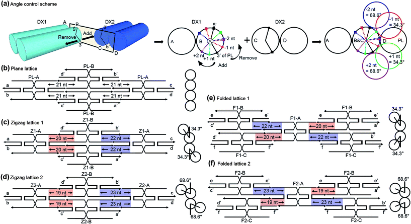 | ||
| Fig. 1 DNA nanostructure design by an angle control scheme (ACS). (a) Isometric (left) and front views (right) of two adjacent double crossover (DX) tiles, DX1 and DX2. When a number of nucleotides is added or removed within the sticky-end region of duplex B, the adjacent DX2 tile is rotated by an angle of 34.3° × N in the clockwise, counter-clockwise direction, respectively. (b–f) Planar figures of various DNA nanostructures made by the ACS; Plane lattice (PL) (b), Zigzag lattices (ZLs) (c and d), Folded lattices (FLs) (e and f), respectively. The PL and ZLs are fabricated by continuous attachment between two different tiles, whereas the FLs consists of three tiles. The blue and red regions represent the nucleotide manipulated sites and side views of each DNA nanostructure are given beside the illustrations. | ||
The simplest ACS-based structures are a plane lattice (PL) and two different zigzag lattices (ZLs). In PL, which is the normal DX lattice, the structure remains planar because no nucleotides were manipulated at the ends of PL tiles (Fig. 1b). In contrast to PL, a nucleotide was manipulated at both ends of the Z1 tiles that are the components of ZL1. This causes the adjacent Z1-B tile to rotate in the clockwise or counter clockwise directions against the Z1-A with an angle of 34.3° along the duplex axis. Therefore, the side view of ZL1 represents a 2D zigzag form with an angle of 34.3° (Fig. 1c). In order to make a steeper shape, we designed the ZL2 with an angle of 68.6° by modifying two nucleotides at the ends of each tile (Fig. 1d). As mentioned above, in order to maintain the overall flatness of ZLs, the same number of nucleotides that were removed in the red regions were then added to the opposite sides of Z1 and Z2 tiles in the blue regions (Fig. 1c and d).
The applicability and versatility of the ACS can be seen in the folded lattices (FLs) that consist of three different tiles. For FL1, one nucleotide is removed from one side of a duplex of F1-A tile and another one is added to the diagonally opposite region. This diagonal manipulation on the other duplex of F1-A creates alternate angle changes on four binding sites with an angle of −34.3° and +34.3°, respectively (see red and blue regions in Fig. 1e). When the manipulated F1-A binds with F1-B and F1-C tiles, they form the repeating building units, and the FL1 is assembled by alternately attaching these building blocks (Fig. S4, ESI†). The same strategy was used for FL2 but it was designed with manipulations of two nucleotides on each side of the F2-A tiles. The side view of FL shows larger projections in directions orthogonal to the lattice plane compared with ZLs and we expected the AFM images of FLs to give distinct topographic features.
To confirm the topographical differences between these five different DNA nanostructure designs, we fabricated samples by annealing the synthetic oligonucleotides and characterizing by atomic force microscopy (AFM) using tapping mode under aqueous buffer. AFM images of each ACS-based structure exhibit large 2D lattice assemblies (Fig. 2). The inset images were obtained by noise-filtered Fourier transform reconstruction showing the periodicities of the lattices (Fig. 2 and Fig. S7, ESI†).9 Although the lattices appear to assemble as designed, we were unable to find sufficient evidence to verify the expected topographical differences within the ACS-based structures in the AFM images. Similar problems have been reported in other systems where AFM imaging of DNA nanostructures appear flatter than expected; this could be due to the strong interaction between the mica substrate and the negatively charged DNA backbone.8,10 Due to the strong Coulomb interactions, the ACS-based 2D lattices collapsed onto the substrate, making it difficult to distinguish between the various designs during height analysis. However, since we do indeed observe very large lattice pieces on the surface, we believe this indicates that the ACS-based 2D lattices likely exist as zigzag and folded sheets within the solution, according to the designs.
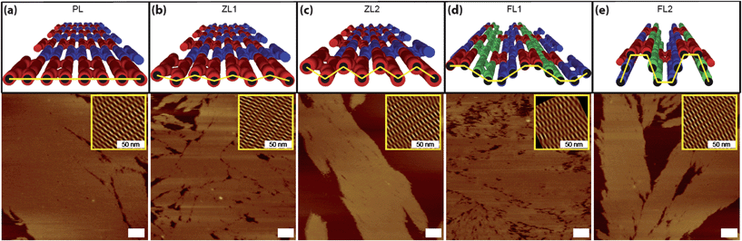 | ||
| Fig. 2 AFM characterization of ACS-based DNA nanostructures. (a–e) Schematic diagrams and their corresponding AFM images of PL (a), ZL1 (b), ZL2 (c), FL1 (d), FL2 (e), respectively. The insets are noise-filtered reconstructed images by fast Fourier transform showing the periodicity of the crystals. Scale bars are 100 nm unless otherwise noted. | ||
In order to verify our understanding of the ACS designs, we built a design intended to form a 1D open tube (OT) structure. This design is somewhat similar to the bent-triple-crossover (BTX) tile structures described previously in the literature.11 In our case a two-tile system was adopted and the OT-A tile was manipulated in a manner similar to that used in the F1-A tile (Fig. 3a). The key point of the OT design that distinguishes it from the previous ACS-based 2D lattices is that there is no nucleotide compensation since we do not wish to maintain overall flatness for a 2D lattice. When the tiles bind each other, the missing nucleotides accumulate continuously such that they cannot form lattice but instead create a tube-like 1D structure. According to the design (Fig. 3b), there should be 9 OT tiles along the circumference of the OT tube leading to an offset of 10 bases leaving the structure as an opened tube structure. The 1D nature of the OT structure was easily observed by AFM (Fig. 3c). The AFM images show the drastically different morphology compared with the ACS-based 2D lattices. Consequently this result suggests that the ACS works properly in the all ACS structures.
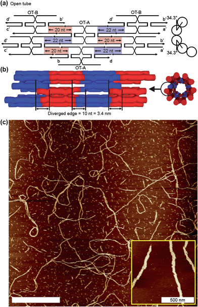 | ||
| Fig. 3 Open tube (OT) structure and its analyses. (a and b) Planar figure and schematic diagram of the OT structure with side views. In contrast with FL structures, there is no nucleotide compensation. This leads to an offset (∼3.4 nm) in both edges of the OT structure thus preventing the structure from forming closed tubes. (c) AFM image of the OT structure. AFM image exhibits dramatically different structures compared with 2D lattice nanostructures. This implies that the ACS design was successful in all the ACS-based DNA nanostructures. The scale bar in the main image is 5 μm. | ||
Experimental section
The design of the tiles was based on the structure of immobile crossover branched junctions and the base sequences used here are given in the Supporting Information in Fig. S1–S6, ESI† and Tables S2–S19, ESI†. Synthetic oligonucleotides were purchased from Integrated DNA Technologies (Coralville, IA, USA) and purified by High-Performance Liquid Chromatography (HPLC). Complexes were formed by mixing a stoichiometric quantity of each strand in physiological 1 × TAE/Mg2+ buffer [Tris-Acetate-EDTA (40 mM Tris, 1 mM EDTA (pH 8.0)) with 12.5 mM magnesium acetate]. For the first step tile annealing, equimolar mixtures of strands were cooled slowly from 95 °C to 25 °C (room temperature) by placing the test tube in 2 L of boiled water in a styrofoam box for at least 24 hours to facilitate hybridization. For the second step lattice annealing, DNA tile mixtures were cooled slowly from 40 °C to 25 °C by placing the test tube in 1 L of water for about 4 hours. After each step of annealing, samples were incubated overnight at 4 °C for structure stabilization. The final concentration of DNA structures was 150 nM. AFM imaging was performed in tapping mode in a 1 × TAE/Mg2+ buffer. A 5 μL annealed-sample was dropped on freshly cleaved mica for 30 seconds. 30 μL of 1 × TAE/Mg2+ buffer was then placed onto the mica and another 5 μL of 1 × TAE/Mg2+ buffer was placed onto the AFM tip. AFM images were obtained on a Digital Instruments Nanoscope III (Vecco, USA) with a multimode fluid cell head in tapping mode under a buffer using NP–S oxide-sharpened silicon nitride tips (Vecco, USA).Conclusions
In conclusion, we have fabricated six different ACS-based DNA superstructures. Although the expected height differences within and between lattice varieties have not been possible to verify using AFM, the available evidence (reliable and large-scale 2D lattice formation by PL, ZL, and FL designs as well as the 1D structure from the OT design) suggests that the ACS designs are forming as designed. Since helical structure is intrinsic to double-stranded DNA, the ACS can be applied not only to tile-based but also other types of DNA structures. The ACS has been shown to be useful for the fabrication of complex DNA structures and may lead to various potential applications by exploiting the binding mechanism to align biomolecules such as streptavidin,6,12 RecA13 and nanomaterials such as metallic, semiconducting or magnetic nanoparticles.14,15 In addition, due to their grooved nature, these ACS structures may aid in the alignment of nanowires, for example carbon nanotube13,16 or polymer wires,17 in parallel arrays along surfaces. Hence, this scheme may be useful in the assembly of nanocircuits for the fabrication of biosensors18 and electronic devices.19Acknowledgements
This work was supported by the research grant from the Korea Sanhak Foundation (KSF-200968) to S. H. Park.Notes and references
- G. M. Whitesides, J. P. Mathias and C. T. Seto, Science, 1991, 254, 1312 CAS.
- D. Philp and J. F. Stoddart, Angew. Chem., Int. Ed. Engl., 1996, 35, 1154 CrossRef.
- S. Förster and T. Plantenberg, Angew. Chem., Int. Ed., 2002, 41, 688 CrossRef.
- N. C. Seeman, Nature, 2003, 421, 427 CrossRef.
- R. Amin, S. Kim, S. H. Park and T. H. LaBean, Nano, 2009, 4, 119 CrossRef CAS.
- E. Winfree, F. Liu, L. A. Wenzler and N. C. Seeman, Nature, 1998, 394, 539 CrossRef CAS.
- P. Yin, R. F. Hariadi, S. Sahu, H. M. T. Choi, S. H. Park, T. H. LaBean and J. H. Reif, Science, 2008, 321, 824 CrossRef CAS.
- (a) Y. He, T. Ye, M. Su, C. Zhang, A. E. Ribbe, W. Jiang and C. Mao, Nature, 2008, 452, 198 CrossRef CAS; (b) D. Han, S. Pal, J. Nangreave, Z. Deng, Y. Liu and H. Yan, Science, 2011, 332, 342 CrossRef CAS.
- W. R. Bowen and T. A. Doneva, J. Membr. Sci., 2000, 171, 141 CrossRef CAS.
- Z. Li, M. Liu, L. Wang, J. Nangreave, H. Yan and Y. Liu, J. Am. Chem. Soc., 2010, 132, 13545 CrossRef CAS.
- A. Kuzuya, R. Wang, R. Sha and N. C. Seeman, Nano Lett., 2007, 7, 1757 CrossRef CAS.
- H. Yan, S. H. Park, G. Finkelstein, J. H. Reif and T. H. LaBean, Science, 2003, 301, 1882 CrossRef CAS.
- K. Keren, R. S. Berman, E. Buchstab, U. Sivan and E. Braun, Science, 2003, 302, 1380 CrossRef CAS.
- J. D. Le, Y. Pinto, N. C. Seeman, K. Musier-Forsyth, T. A. Taton and R. A. Kiehl, Nano Lett., 2004, 4, 2343 CrossRef CAS.
- S. Pal, Z. Deng, B. Ding, H. Yan and Y. Liu, Angew. Chem., Int. Ed., 2010, 49, 2700 CAS.
- H. T. Maune, S. P. Han, R. D. Barish, M. Bockrath, W. A. Goddard, III, R. W. K. Rothermund and E. Winfree, Nat. Nanotechnol., 2010, 5, 61 CrossRef CAS.
- Y. Eichen, E. Braun, U. Sivan and G. Ben-Yoseph, Acta Polym., 1998, 49, 663 CrossRef CAS.
- I. H. Stein, C. Steinhauer and P. Tinnefeld, J. Am. Chem. Soc., 2011, 133, 4193 CrossRef CAS.
- K. Keren, R. S. Berman, E. Buchstab, U. Sivan and E. Braun, Science, 2003, 302, 1380 CrossRef CAS.
Footnote |
| † Electronic supplementary information (ESI) available: Detailed materials, methods, and descriptions of synthesizing process of folded structures, DNA sequences, additional AFM images and their analyses are provided. See DOI: 10.1039/c1sm06379k |
| This journal is © The Royal Society of Chemistry 2012 |