An aqueous soaking treatment for efficient polymer solar cells†
Hui
Li
abc,
Zhaobin
Chen
a,
Haowei
Tang
abc,
Wentao
Xu
abc,
Jun
Li
abc,
Xiaoli
Zhao
abc and
Xiaoniu
Yang
*ab
aPolymer Composites Engineering Laboratory, Changchun Institute of Applied Chemistry, Chinese Academy of Sciences, Renmin St. 5625, Changchun, 130022, P.R. China. E-mail: xnyang@ciac.jl.cn; Fax: +86-431-8526 2028; Tel: +86-431-8526 2838
bState Key Laboratory of Polymer Physics and Chemistry, Changchun Institute of Applied Chemistry, Chinese Academy of Sciences, Renmin St. 5625, Changchun, 130022, P.R. China
cGraduate School of the Chinese Academy of Sciences, Beijing, 100049, P.R. China
First published on 28th August 2012
Abstract
Polymer solar cells, which convert clean renewable solar energy into electricity, have been considered as most promising technology. It is well recognized that the power conversion efficiency of the cell device greatly depends on the morphology of the polymer active layer, and the post-treatments commonly used, such as energy consuming thermal annealing and solvent vapor treatment, are not suitable for commercial applications on large-area polymer solar cells. Herein, we propose a facile aqueous solution post-treatment, which involves only water and a small amount of carbon disulfide (0.13 wt% of CS2), based on regioregular poly (3-hexylthiophene) (P3HT) and [6, 6]-phenyl-C61-butyric acid methyl ester (PCBM) blend film to improve the active layer morphology and increase the device efficiency. Upon soaking the blend film in the aqueous solution, P3HT crystallinity is increased and an optimum morphology of nanoscale phase separation with an interpenetrating network is constructed, which offers percolating pathways for charge carrier transport. Furthermore, AFM and XPS analyses reveal that a coarser structure with heave-like PCBM-rich domains is built up at the active layer/cathode (top) interface, which improves the contact with the metal cathode for efficient electron transportation and collection. The feasibility of this method is verified by J–V characteristic of the photovoltaic device, which demonstrates an increased PCE of 3.09% compared with 1.84% of the pristine device, indicating its potential implementation on the application of large-area polymer solar cells.
Introduction
Due to their mechanical flexibility, lightweight, low-cost and easy manufacturing process, polymer solar cells have been considered as a most promising technology to convert clean renewable solar energy into electricity. In recent decades, bulk heterojunction (BHJ) blends of poly (3-hexylthiophene) (P3HT) as electron donor material and [6, 6]-phenyl-C61-butyric acid methyl ester (PCBM) as electron acceptor material, which exhibit relatively high carrier mobility,1,2 have gained extensive scientific research. While the efficiency of polymer photovoltaic devices based on P3HT/PCBM blend film greatly depends on the morphology structure of the film,3,4 such as the degree of P3HT crystallinity,5,6 length scale phase separation between polymer and fullerene components,7,8 and vertical phase separation along the film,9etc.In the photoelectric conversion process, a sequence of four steps converts incident solar illumination to photocurrent: exciton formation after photon absorption, exciton diffusion and dissociation into charge carriers, charge carrier transportation, and collection of charge at the corresponding electrodes.10,11 First of all, the exciton generation efficiency largely depends on the optical absorption of the active layer, which requires high P3HT crystallinity in the BHJ of the P3HT/PCBM thin film for efficient light harvesting.12 On the other hand, because the effective exciton diffusion length is limited to 10 nm and the dissociation occurs at the donor/acceptor interfaces, nanoscale phase separation with a large interface area is necessary for efficient exciton diffusion and dissociation into a hole and electron.7 However, due to the abundance of donor/acceptor interface, carrier recombination probably occurs during the carrier transportation process. Thus a separated percolating network of polymer and fullerene components is required for efficient carrier transportation and minimum recombination loss.11 Besides, high carrier mobility with improved P3HT crystallinity and the vertical phase separation with PCBM and P3HT enriched at the active layer/metal cathode (top) surface and active layer/ITO anode (bottom) surface, respectively, are favorable for efficient carrier transport to the corresponding electrodes.9 At the same time, this vertical phase segregation also enhances contact between the active layer and the corresponding electrodes, contributing to improve carrier collection efficiency. From above descriptions we can see that, high P3HT crystallinity, nanoscale phase separation with interpenetrating network, and vertical phase separation with individual component enrichment at the top or bottom surface are ideal for efficient photovoltaic devices.
In order to approach the ideal morphology of the active layer, different post-treatment methods, such as post thermal annealing and solvent vapor treatment, are proposed during the fabrication process of polymer solar cells. Although power conversion efficiency (PCE) of the photovoltaic device is increased via thermal annealing treatment, energy consumption and instability of the blend film due to PCBM aggregation 13,14 hamper its commercial application. While for the solvent vapor treatment,15–17 the organic solvents used, such as chloroform, chlorobenzene, and tetrahydrofuran, are volatile and flammable, which are not suitable for large-area roll-to-roll fabrication of polymer solar cells. Recently, water-soluble materials have been applied to the photovoltaic device as the active layer18–21 or cathode interface materials22,23 with improved device efficiency, which made a solid step towards the large-scale application of polymer solar cells.24,25
In the present study, we propose a facile aqueous solution soaking post-treatment, which involves only water and a small amount of CS2 (0.13wt%), to optimize the morphology of the P3HT/PCBM active layer. Upon immersing in H2O/CS2 aqueous solution, P3HT crystallinity increases, and the nanoscale phase separation and vertical phase separation are constructed. Correspondingly, the PCE of photovoltaic device increases from 1.84% to 3.09%. Compared with other post-treatment technologies, this new efficient treatment method is easily processible and low energy consuming, exhibiting potential implementation on the commercial application of large-area roll-to-roll polymer solar cells.
Experimental details
Materials
Regioregular poly (3-hexylthiophene) (P3HT) (RR = 95%, Mn = 22 000) was purchased from Luminescence Technology Co. [6, 6]-phenyl-C61-butyric acid methyl ester (PCBM) and o-dichlorobenzene (ODCB, anhydrous, 99%) were acquired from Sigma-Aldrich Co.. Carbon disulfide (CS2) and 1, 8-octanedithiol (OT) were obtained from Sinopharm Chemical Reagent Co. and Alfa Aesar Co., respectively.Sample preparation
P3HT/PCBM (1:1, w:w) blends were dissolved in ODCB overnight with P3HT concentration of 10 mg/ml. The H2O/CS2 aqueous solution was prepared by ultrasonic agitation in a sealed conical flask. After that, spin coated P3HT/PCBM film was immersed in solution under sealed conditions, and then dried with nitrogen flow. CS2 weight concentration (denoted as CS2 wt%) in the aqueous solution was 0.05 wt%, 0.10 wt%, 0.13 wt%, and 0.16 wt%, respectively.The bottom surface of film was acquired by floating-off method. In this process, water was used to float-off the film and the floating film was then transferred to the silicon substrate with the bottom surface on top for atomic force microscopy (AFM) and X-ray photoelectron spectroscopy (XPS) measurements. For the transmission electron microscopy (TEM) analysis, the film was immersed in water and then floated onto a copper grid.
To thoroughly investigate PCBM distribution and aggregation in the active layer, an etching technique was used to selectively dissolve the PCBM component in P3HT/PCBM blend film. In this process, OT, which is a good solvent for PCBM but a poor solvent for P3HT, was dropped on the sample film for 5 seconds, and then rinsed with water. After that, the treated film was dried with nitrogen flow and ready for AFM analysis.
Measurements
UV-Vis absorption spectra were recorded on a Lambda 750 spectrometer (Perkin-Elmer, Wellesley, MA).X-ray diffraction (XRD) profiles were obtained using a Bruker D8 Discover Reflector with X-ray generation power of 40 kV tube voltage and 40 mA tube current. The diffraction was acquired at a θ–2θ symmetry within the range of 2θ = 3°–30°.
TEM was performed on a JEOL JEM-1011 transmission electron microscope and operated at an acceleration voltage of 100 kV.
Surface morphology of the film was characterized on an Agilent 5500 AFM by tapping mode in ambient atmosphere.
XPS measurement was performed on VG ESCALAB MK II X-ray photoelectron spectroscope and the sample depth was less than 10 nm.
The J–V characteristics of photovoltaic cells were performed in a glove box under the illumination at 100 mW cm−2 using an AM1.5 G solar simulator.
Device fabrication
In a typical device fabrication process, the indium tin oxide (ITO) substrate was cleaned by ultrasonic agitation with deionized water, iso-propanol, and acetone, and subsequently treated in a UV–ozone oven for 20 min to remove organic residue on the surface. The PEDOT: PSS layer was spin-coated at 2000 rpm for 1 min and baked at 150 °C for 10 min. And then deionized water was rinsed on the layer with 3000 rpm for 1 min to remove PSS component26 and the resulting layer was annealed at 150 °C for 10 min, which could minimize PEDOT![[thin space (1/6-em)]](https://www.rsc.org/images/entities/char_2009.gif) :PSS solubility in water to avoid film lifting-off in the following soaking treatment. Subsequently, P3HT/PCBM active layer (thickness ∼100 nm) was spin-coated on the substrate and then immersed in the prepared H2O/CS2 aqueous solution under ambient atmosphere. After drying with nitrogen flow, LiF buffer layer (thickness ∼1 nm) and Al cathode (thickness ∼80 nm) were deposited on the active layer by vacuum deposition with vacuum lower than 5.0 × 10⁻⁴ Pa. The active surface area of the device was 0.09 cm2.
:PSS solubility in water to avoid film lifting-off in the following soaking treatment. Subsequently, P3HT/PCBM active layer (thickness ∼100 nm) was spin-coated on the substrate and then immersed in the prepared H2O/CS2 aqueous solution under ambient atmosphere. After drying with nitrogen flow, LiF buffer layer (thickness ∼1 nm) and Al cathode (thickness ∼80 nm) were deposited on the active layer by vacuum deposition with vacuum lower than 5.0 × 10⁻⁴ Pa. The active surface area of the device was 0.09 cm2.
Results and discussion
Optical absorption of the blend film
Fig. 1(a) shows the UV-Vis absorption spectra of P3HT/PCBM blend films soaking treated with aqueous solutions containing 0.05 wt%, 0.10 wt%, 0.13 wt%, and 0.16 wt% of CS2, respectively, and the pristine film is also included for comparison. For pristine P3HT/PCBM film, four peaks are clearly observed. Among them, the first one at around 333 nm comes from PCBM, the other three peaks centered at 512 nm, 554 nm, and 607 nm, are caused by P3HT, which correspond to the absorption of ordered stacked P3HT backbones and interchain π–π stacking of P3HT molecules in the film. After aqueous solution soaking treatment, the main peak absorbance shows a red-shift from 512 nm to 517 nm, which indicates the extended mean conjugated length of P3HT.27 Furthermore, the absorption intensity at around 607 nm apparently increases with increased CS2 amount, which demonstrates that P3HT crystallinity is improved.15,28 From this figure one can also see that, after CS2 reaches 0.10 wt%, the intensity of the absorption peak at 607 nm increases indistinctively, implying that the degree of P3HT crystallinity becomes saturated at this concentration. When large amounts of CS2 are added in the aqueous solution, for example, more than 0.16 wt%, CS2 is not completely soluble in water and the blend film would be dissolved during the soaking process. | ||
| Fig. 1 (a) UV-Vis spectra and (b) X-ray diffraction (XRD) profiles of pristine and treated P3HT/PCBM blend films with H2O/CS2 aqueous solution containing different CS2 concentrations for 1 min. | ||
The improvement of P3HT crystallinity is further confirmed by X-ray diffraction (XRD) analysis, as shown in Fig. 1(b). The pristine P3HT/PCBM film gives one main peak at around 2θ = 5.4°, which belongs to the crystallographic (100) of P3HT.5,29 After soaking treatment, the peak position does not change, but the intensity greatly increases, especially in the case of the aqueous solution with CS2 concentration higher than 0.05 wt%, indicating that P3HT crystallinity is improved in agreement with the UV-Vis results. Again, if CS2 concentration further increases to higher than 0.10 wt%, the peak intensity does not change a lot. Combining UV-Vis and XRD analyses, it is believed that the soaking treatment is effective to increase P3HT crystallinity. To ensure sufficient treatment, 0.13 wt% of CS2 concentration in the aqueous solution is used to investigate the morphology of the active layer in the following sections (The treating time is set to 1 min according to the PCE vs. treating time variation, see Fig. S1†).
Structural properties of the active layer
Characteristic bright-field transmission electron microscopy (BF-TEM) images and corresponding selected-area electron diffraction (SAED) patterns of P3HT/PCBM active layers without and with soaking treatment (CS2 0.13 wt%) are presented in Fig. 2. Due to a lower density property, P3HT appears as bright regions, and the dark regions are attributed to PCBM-rich phases. For the pristine film, as shown in Fig. 2(a), we can only observe some short bright fibrillar P3HT crystals and a weak outer diffraction ring in the SAED pattern, which attributes to the crystallographic (020) reflection of P3HT chains,7 indicating a low degree of P3HT crystallinity. In contrast, the treated film exhibits numerous bright fibrillar P3HT crystals densely overlapped with each other over the whole film, implying the increase in P3HT crystallinity after immersing in aqueous solution, which is also evidenced by the stronger intensity of P3HT (020) reflection ring in Fig. 2(b). In addition, PCBM is promoted to diffuse and aggregate, as shown in Fig. 2(b), to form irregular PCBM-rich domains with size of 70 nm and larger regions (∼500 nm), which indicates the improved nanoscale phase separation between crystalline P3HT and aggregated PCBM. From the above descriptions, it is found that upon aqueous solution soaking treatment, P3HT crystallinity is improved and the nanoscale phase separation with interpenetrating network is constructed, which offer interpenetrating pathways for charge carrier transportation. (The blend films treated with aqueous solutions containing different CS2 concentration also show the same morphology, see Fig. S2†). | ||
| Fig. 2 Bright-field transmission electron microscopy (BF-TEM) images and corresponding selected-area electron diffraction (SAED) patterns of pristine (a) and soaking treated film in H2O/CS2 aqueous solution with CS2 concentration of 0.13 wt% for 1 min (b). | ||
The detailed morphologies of P3HT/PCBM films before and after treatment were further characterized by atomic force microscopy (AFM), as shown in Fig. 3. For the pristine film, Fig. 3(a–d) show almost the same surface morphology that no phase separation is observed and P3HT fibrils homogeneously distributed over both the active layer/metal cathode (top) surface and active layer/ITO anode (bottom) surface.
 | ||
| Fig. 3 Tapping mode AFM topography (a, c, e, g) and phase (b, d, f, h) images of the composite films: pristine film with the top (a, b) and bottom surfaces (c, d), aqueous solution soaking treated film (CS2 0.13 wt%) with the top (e, f) and bottom surfaces (g, h). | ||
The same situation also occurs on the bottom surface of the P3HT/PCBM film treated with aqueous solution containing 0.13 wt% of CS2 (Fig. 3g and h), implying that the soaking treatment does not affect the bottom surface morphology of the blend film. Interestingly, phase separation is clearly observed on the top surface of the treated film, as shown in Fig. 3e and f, in which a coarser structure of uniformly distributed heave-like aggregates with the size of 50–100 nm is constructed, and the aggregates are ∼15 nm in height. These heave-like aggregates are believed to be PCBM component because the pure PCBM film shows apparent aggregation while no change was observed in pure P3HT film before and after soaking treatment under the same conditions (see Fig. S3†).
To further identify the composition of the aggregates on the top surface of the soaking treated P3HT/PCBM blend film, 1,8-octanedithiol (OT), which is a good solvent for PCBM but poor solvent for P3HT, is used to selectively dissolve PCBM component in the blend film.30,31 Compared with the soaking treated film without OT etching (Fig. 3e and f), the etched film shows totally different morphology, as shown in Fig. 4. After etching PCBM phase from the soaking treated film, the heave-like aggregates disappear (Fig. 4a), and the phase image also shows no aggregates and phase separation (Fig. 4b). Instead, exposed P3HT network composed of fibrillar P3HT nanowhiskers overlapped with each other on the whole film is presented. Meanwhile, the OT etching does not change the topography of soaking treated pure P3HT film (Fig. S4†) and UV-Vis analysis shows that the peak at 333 nm disappears (Fig. S5†), which indicate that the morphology changes before and after OT etching could only be resulted from PCBM component dissolution. This PCBM aggregation on the active layer/cathode interface is beneficial for efficient electron collection which enhances the contact between active layer and cathode.
 | ||
| Fig. 4 AFM topography (a) and phase (b) images of soaking treated P3HT/PCBM film after OT etching on the top surface. | ||
Vertical phase separation
To further verify the distribution of P3HT and PCBM components along the vertical direction, X-ray photoelectron spectroscopy (XPS) is used to calculate the S/C element ratios on the top and bottom surfaces of the pristine and soaking treated P3HT/PCBM blend films, in which the S (2p) originates from P3HT while C (1s) represents both P3HT and PCBM components (Fig. S6†).30 The variation trend of S/C ratios which are proportionally correlated to the percentage of P3HT in the composite is given in Fig. 5. From these results it can be seen that, for the pristine film, the S/C ratio at the top surface is much higher than that at the bottom surface (0.0968 vs. 0.0392). The relatively lower P3HT (26.9 mNm−2) surface energy than PCBM (37.8 mNm−2) is responsible for this P3HT enrichment, because the P3HT component is preferred to enrich on the top surface to minimize the overall energy of free surface during the spin-casting process.32 After soaking treatment, the S/C value at the bottom surfaces is almost unchanged (0.0392 to 0.0395), suggesting that the soaking treatment has almost no effect on the active layer/ITO interface. The result is in agreement with the AFM analysis. However, the S/C ratio at the top surface significantly decreases from 0.0968 to 0.0823, which further demonstrates PCBM enrichment on the top surface after soaking treatment, as above observed by AFM measurement. Combined with the PCBM aggregation in AFM observation, it is reasonable that the vertical phase separation with PCBM enriched on the top surface in P3HT/PCBM blend film is constructed through aqueous solution soaking treatment. | ||
| Fig. 5 Element composition at the top and bottom surfaces of the pristine and soaking treated P3HT/PCBM blend films. | ||
Photovoltaic performance
To evaluate the effect of morphology changes on the performance of devices, BHJ-type PSCs (ITO/PEDOT:PSS/P3HT/PCBM/LiF/Al) were fabricated and their performances were measured under illumination at 100 mWcm−2 (AM 1.5G). Fig. 6(a) shows the current density–voltage (J–V) curves of the pristine and soaking treated devices with H2O/CS2 aqueous solution containing different CS2 concentration, and the corresponding values are listed in Table 1. From Table 1, we could see that the pristine device exhibits power conversion efficiency (PCE) of 1.84%, while 2.35% of the PCE is obtained for the device treated with aqueous solution containing 0.05 wt% of CS2. The efficiency of the solar cells increases with the increase of CS2 amount in solution, and maximum PCE is reached at 3.09% for the device treated in aqueous solution with 0.13 wt% CS2. These results show that the aqueous solution treatment significantly improves the PCE of the devices based on P3HT/PCBM blend film. Meanwhile, the current density (Jsc) and the fill factor (FF) show the similar variation trend, while open-circuit voltage (Voc) slightly decreases from 0.61 to 0.58, which probably relates to the shift of P3HT HOMO energy level due to the increased P3HT crystallinity.33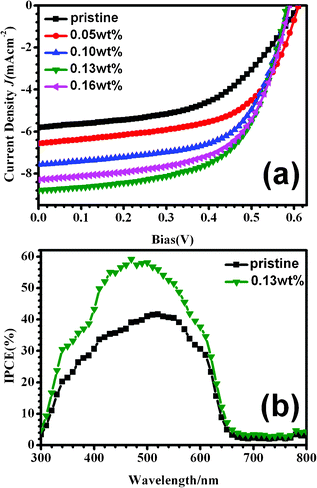 | ||
| Fig. 6 (a) Current density–voltage (J–V) characteristics and (b) incident photon-to-electron conversion efficiency (IPCE) of photovoltaic devices composed of pristine and soaking treated P3HT/PCBM active layers with H2O/CS2 aqueous solution for 1 min. | ||
| PV device parameters | Jsc/mA cm−2 | Voc/V | FF | PCE(%) |
|---|---|---|---|---|
| Pristine | 5.82 | 0.61 | 0.52 | 1.84 |
| 0.05 wt% | 6.57 | 0.61 | 0.59 | 2.35 |
| 0.01 wt% | 7.58 | 0.59 | 0.61 | 2.74 |
| 0.13 wt% | 8.80 | 0.58 | 0.61 | 3.09 |
| 0.16 wt% | 8.29 | 0.59 | 0.61 | 2.97 |
The corresponding incident photon-to-electron conversion efficiency (IPCE) is given in Fig. 6(b), and the aqueous solution treated device with 0.13 wt% of CS2 concentration is selected as a typical example to compare with the pristine device. The pristine device possesses an IPCE spectrum lower than 40% within the entire spectrum range. In contrast, the treated device shows an enhanced IPCE spectrum, which becomes remarkable in the range of 300–650 nm, and the maximum conversion efficiency of 60% occurs at around 500 nm. The IPCE data indicate that the photo absorption and photocurrent are enhanced by the aqueous solution treatment.
Discussions
From the above descriptions it can be seen that, the H2O/CS2 aqueous solution soaking treatment is effective for the morphology optimization of P3HT/PCBM blend film and performance improvement of photovoltaic devices. We speculate that the morphology improvement is mainly attributed to two aspects: the mobility of P3HT and PCBM molecules upon interaction with CS2 and the hydrophobic interaction of PCBM molecules with water. Upon immersing the film in H2O/CS2 aqueous solution, CS2, which is good solvent for both P3HT and PCBM, will gradually penetrate into the polymer film. During this process, as a small molecule, PCBM molecule is activated to diffuse, while P3HT segment becomes mobile to some extent,8,34 resulting in the enhanced P3HT crystallinity and P3HT/PCBM phase separation, as observed by UV-Vis, TEM, and AFM analyses. In addition, with the hydrophobic repulsion interactions with water,35,36 diffused PCBM aggregates and forms PCBM-rich domains, which is demonstrated by TEM and AFM measurements. Moreover, because of the presence of the low CS2 concentration gradient from the top to the bottom surfaces of the films, the PCBM aggregation and the nanoscale phase separation are apparent on the top surface, which results in a coarser structure with the heave-like topography at the top surface but almost unchanged morphology at the bottom surface. These two reasons lead to the formation of vertical phase separation with PCBM enriched on the top surface, which not only promotes the charge carrier transportation, but also enhances the contact between the PCBM and LiF/Al cathode to increase the electron collection efficiency.Consistent with the morphology improvement, the device soaking treated with CS2 0.13 wt% shows a significant increase of Jsc from 5.82 to 8.80 mA cm−2, which is mainly attributed to the enhanced optical absorption of the film and the improvement of P3HT crystallinity.12 Moreover, it is obvious that FF is increased from 0.52 to 0.61 upon immersing treatment, which is associated with the improved cathode/active layer contact interface and morphology optimization.37 Although Voc decreases slightly, we still obtain an improved PCE of 3.09%, which indicates the feasibility of this aqueous solution post-treatment on the bulk heterojunction solar cell. Compared with other post-treatment, this aqueous solution soaking treatment is low energy consuming, which promotes the development of fabrication process of large-area polymer solar cells. And it is believed that the PCE of the treated photovoltaic devices could be further improved by adjusting the treatment parameters, including selecting other proper organic solvents, tailoring the treatment temperature, etc.
Conclusions
We propose a facile aqueous solution post-treatment, which involves only water and a small amount of CS2 (0.13 wt%), to improve the morphology of active layer and increase PCE of photovoltaic device based on P3HT/PCBM blend film. Upon H2O/CS2 aqueous solution soaking treatment, P3HT crystallinity is increased, nanoscale phase separation with interpenetrating network is generated, and vertical phase separation with PCBM enriched at the active layer/cathode interface is constructed. All these factors are favorable for photoelectric conversion. The J–V characteristic of photovoltaic devices based on treated P3HT/PCBM active layer shows PCE of 3.09%, which is greatly increased in comparison with 1.84% of pristine one. As an easily processible and low energy consuming method, this aqueous solution soaking technology exhibits potential implementation on the fabrication process of large-area polymer solar cells.Acknowledgements
This work was financially supported by the National Natural Science Foundation of China (Grant No. 20874100, 20925415, 20990233). X.N.Y. would like to thank the Hi-Tech Research and Development Program (863) of China (2011AA050524), the Fund for Creative Research Groups (Grant No. 50921062), and Solar Energy Initiative (Grant No. KGCX2-YW-399+9) of the Chinese Academy of Sciences for financial support.References
- H. Sirringhaus, N. Tessler and R. H. Friend, Science, 1998, 280, 1741 CrossRef CAS.
- V. D. Mihailetchi, J. K. J. van Duren, P. W. M. Blom, J. C. Hummelen, R. A. J. Janssen, J. M. Kroon, M. T. Rispens, W. J. H. Verhees and M. M. Wienk, Adv. Funct. Mater., 2003, 13, 43 CrossRef CAS.
- X. Yang and J. Loos, Macromolecules, 2007, 40, 1353 CrossRef CAS.
- L. M. Chen, Z. R. Hong, G. Li and Y. Yang, Adv. Mater., 2009, 21, 1434 CrossRef CAS.
- S. Nam, M. Shin, H. Kim and Y. Kim, Nanoscale, 2010, 2, 2384 RSC.
- T. Agostinelli, S. Lilliu, J. G. Labram, M. Campoy-Quiles, M. Hampton, E. Pires, J. Rawle, O. Bikondoa, D. D. C. Bradley, T. D. Anthopoulos, J. Nelson and J. E. Macdonald, Adv. Funct. Mater., 2011, 21, 1701 CrossRef CAS.
- X. N. Yang, J. Loos, S. C. Veenstra, W. J. H. Verhees, M. M. Wienk, J. M. Kroon, M. A. J. Michels and R. A. J. Janssen, Nano Lett., 2005, 5, 579 CrossRef CAS.
- M. A. Ruderer, S. Guo, R. Meier, H. Y. Chiang, V. Korstgens, J. Wiedersich, J. Perlich, S. V. Roth and P. Muller-Buschbaum, Adv. Funct. Mater., 2011, 21, 3382 CrossRef CAS.
- M. Campoy-Quiles, T. Ferenczi, T. Agostinelli, P. G. Etchegoin, Y. Kim, T. D. Anthopoulos, P. N. Stavrinou, D. D. C. Bradley and J. Nelson, Nat. Mater., 2008, 7, 158 CrossRef CAS.
- P. W. M. Blom, V. D. Mihailetchi, L. J. A. Koster and D. E. Markov, Adv. Mater., 2007, 19, 1551 CrossRef CAS.
- P. Heremans, D. Cheyns and B. P. Rand, Acc. Chem. Res., 2009, 42, 1740 CrossRef CAS.
- P. Vanlaeke, A. Swinnen, I. Haeldermans, G. Vanhoyland, T. Aernouts, D. Cheyns, C. Deibel, J. D'Haen, P. Heremans, J. Poortmans and J. V. Manca, Sol. Energy Mater. Sol. Cells, 2006, 90, 2150 CrossRef CAS.
- X. N. Yang, A. Alexeev, M. A. J. Michels and J. Loos, Macromolecules, 2005, 38, 4289 CrossRef CAS.
- B. Watts, W. J. Belcher, L. Thomsen, H. Ade and P. C. Dastoor, Macromolecules, 2009, 42, 8392 CrossRef CAS.
- H. W. Tang, G. H. Lu, L. G. Li, J. Li, Y. Z. Wang and X. N. Yang, J. Mater. Chem., 2010, 20, 683 RSC.
- G. H. Lu, L. G. Li and X. N. Yang, Small, 2008, 4, 601 CrossRef CAS.
- J. H. Park, J. S. Kim, J. H. Lee, W. H. Lee and K. Cho, J. Phys. Chem. C, 2009, 113, 17579 CrossRef CAS.
- J. K. Mwaura, M. R. Pinto, D. Witker, N. Ananthakrishnan, K. S. Schanze and J. R. Reynolds Jr., Langmuir, 2005, 21, 10119 CrossRef CAS.
- J. H. Yang, A. Garcia and T. Q. Nguyen, Appl. Phys. Lett., 2007, 90, 103514 CrossRef.
- D. Izuhara and T. M. Swager, J. Am. Chem. Soc., 2009, 131, 17724 CrossRef CAS.
- Z. Y. Liu, L. J. Liu, H. Li, Q. F. Dong, S. Y. Yao, A. B. Kidd, X. Y. Zhang, J. Y. Li and W. J. Tian, Sol. Energy Mater. Sol. Cells, 2012, 97, 28 Search PubMed.
- Z. C. He, C. M. Zhong, X. Huang, W. Y. Wong, H. B. Wu, L. W. Chen, S. J. Su and Y. Cao, Adv. Mater., 2011, 23, 4636 CrossRef CAS.
- K. Yao, L. Chen, Y. W. Chen, F. Li and P. S. Wang, J. Mater. Chem., 2011, 21, 13780 RSC.
- R. Sondergaard, M. Hosel, D. Angmo, T. T. Larsen-Olsen and F. C. Krebs, Mater. Today, 2012, 15, 36 CrossRef CAS.
- M. Jorgensen, K. Norrman, S. A. Gevorgyan, T. Tromholt, B. Andreasen and F. C. Krebs, Adv. Mater., 2012, 24, 580 CrossRef.
- D. M. DeLongchamp, B. D. Vogt, C. M. Brooks, K. Kano, J. Obrzut, C. A. Richter, O. A. Kirillov and E. K. Lin, Langmuir, 2005, 21, 11480 CrossRef CAS.
- Y. D. Park, H. S. Lee, Y. J. Choi, D. Kwak, J. H. Cho, S. Lee and K. Cho, Adv. Funct. Mater., 2009, 19, 1200 CrossRef CAS.
- L. G. Li, G. H. Lu and X. N. Yang, J. Mater. Chem., 2008, 18, 1984 RSC.
- Z. Yu, H. Yan, K. Lu, Y. J. Zhang and Z. X. Wei, RSC Adv., 2012, 2, 338 RSC.
- Z. Xu, L. M. Chen, G. W. Yang, C. H. Huang, J. H. Hou, Y. Wu, G. Li, C. S. Hsu and Y. Yang, Adv. Funct. Mater., 2009, 19, 1227 CrossRef CAS.
- J. K. Lee, W. L. Ma, C. J. Brabec, J. Yuen, J. S. Moon, J. Y. Kim, K. Lee, G. C. Bazan and A. J. Heeger, J. Am. Chem. Soc., 2008, 130, 3619 CrossRef CAS.
- D. S. Germack, C. K. Chan, B. H. Hamadani, L. J. Richter, D. A. Fischer, D. J. Gundlach and D. M. DeLongchamp, Appl. Phys. Lett., 2009, 94, 233303 CrossRef.
- K. Vandewal, A. Gadisa, W. D. Oosterbaan, S. Bertho, F. Banishoeib, I. Van Severen, L. Lutsen, T. J. Cleij, D. Vanderzande and J. V. Manca, Adv. Funct. Mater., 2008, 18, 2064 CrossRef CAS.
- T. Erb, U. Zhokhavets, G. Gobsch, S. Raleva, B. Stuhn, P. Schilinsky, C. Waldauf and C. J. Brabec, Adv. Funct. Mater., 2005, 15, 1193 CrossRef CAS.
- L. W. Li, D. Bedrov and G. D. Smith, J. Chem. Phys., 2005, 123, 204504 CrossRef.
- R. Ludwig and A. Appelhagen, Angew. Chem., Int. Ed., 2005, 44, 811 CrossRef CAS.
- D. Gupta, S. Mukhopadhyay and K. S. Narayan, Sol. Energy Mater. Sol. Cells, 2010, 94, 1309 CrossRef CAS.
Footnote |
| † Electronic Supplementary Information (ESI) available. See DOI: 10.1039/c2ra21193a |
| This journal is © The Royal Society of Chemistry 2012 |