Acid-treated SWCNT/polyurethane nanoweb as a stretchable and transparent Conductor†
Tae
Ann Kim
,
Sang-Soo
Lee
,
Heesuk
Kim
and
Min
Park
*
Photo-electronic Hybrids Research Center, Korea Institute of Science and Technology, Seoul 136-791, Korea. E-mail: minpark@kist.re.kr; Fax: +82-2-958-5309; Tel: +82-2-958-5334
First published on 3rd October 2012
Abstract
To obtain carbon-nanotube (CNT) conductors with high conductance and transmittance, well-connected conducting paths must be formed with a relatively small number of CNTs. In this study, we employed electrospun polyurethane (PU) nanofibers to guide the deposition of CNTs at desired locations, which makes it possible to acquire high conductivity at low concentrations of CNTs. PU has an affinity for CNTs and inherently elastic characteristics; thus, it can be applied as a stretchable scaffold for CNT deposition. A sample fabricated by nine dipping-and-washing cycles in acid-treated single-walled CNT (a-SWCNT) solution and distilled water, followed by doping, exhibited a sheet resistance of 424 Ω sq−1 at 63%T. When we measured the resistance of a-SWCNT/PU conductors under a wide range of strains (up to 100%), their change in resistance was reduced as more stretching/releasing cycles were applied. In addition, these variations in resistance according to the number of stretching cycles could be significantly reduced when dipping and doping processes were performed using a pre-stretched PU nanoweb. After more than six stretching cycles, the resistance under a tensile strain of up to 100% remained nearly stable at a value of 8.15 kΩ. Our results demonstrate an effective way of preparing a transparent and stretchable conductor with stable performance during repetitive stretching and releasing.
Introduction
Stretchability in electronics allows the development of many devices that are not feasible with traditional electronics technology, such as flexible displays,1,2 sensor skins,3,4 eyeball cameras,5 and implantable devices.6–8 One of the major challenges to create stretchable electronics is developing materials that can absorb large amounts of strain without fracture or significant degradation in their electronic properties. One strategy to realize stretchable electronics is to form inorganic materials in wavy or interconnected structures by incorporating a pre-strained elastic substrate.9–11 Alternatively, new materials that are both elastic and electro-conductive have been developed in the form of polymer composites containing conductive fillers.12Carbon nanotubes (CNTs) possess high aspect ratios as well as outstanding conductivity and mechanical properties, which makes them promising materials for stretchable conductors; randomly distributed CNT films remain conductive even under linear strains of 700%.13 Recently, elastic conductors composed of a single-walled CNT (SWCNT)/imidazolium-based ionic liquid/fluorinated copolymer14,15 or Ag flakes/multi-walled carbon nanotubes decorated with Ag nanoparticles/polyvinylidene fluoride16 showed high conductivities, up to 102 or 5710 S cm−1, respectively. However, the conductivity of these composites was significantly degraded when they were stretched. Additionally, they required additional mechanical processing to increase their level of strain because the addition of a large amount of conductive filler can enhance the conductivity but reduce the mechanical strain. To overcome these disadvantages, well-aligned CNT ribbons embedded in poly(dimethylsiloxane) were reported and exhibited stable conductivity under repetitive linear tensile strains of up to 100%.17
Electrospinning is one of the most powerful techniques used to produce continuous nano-sized one-dimensional structures by employing a strong electrical field to draw very fine fibers from liquid sources of polymers, oxides, and metals.18 The fibers are typically collected in the form of a non-woven net, which can be used in a wide range of applications, including semi-permeable membranes, filters, and scaffolds for tissue engineering. In particular, electrospun polymer nanofibers can be used as templates to create a continuously connected two-dimensional network of nanomaterials without agglomeration.19,20 Additionally, this web structure enables stiff and non-stretchable materials to conform to three-dimensional surfaces and to show omnidirectional extension.4
The formation of well-connected conducting paths with a relatively small number of CNTs is an important factor for producing high-quality conductors possessing high transmittance. In this study, we prepared electrospun nanowebs consisting of elastic nanofibers that have attractive interactions with CNTs and used them as a template to assist in the deposition of CNTs at desired locations. The self-assembly of CNTs is achieved by dipping nanowebs into the CNT ink. This leads to a percolated structure even at low concentrations of CNTs, allowing highly conductive and transparent conductors to be made. Elastic nanofibers also help to preserve the conducting paths of CNTs under large strains. CNT thin films exhibit a drastic reduction in conductivity because some of the conducting pathways are broken down and the number of low-conducting regions increases.13 To enhance the conductivity of those conductors, chemical doping was carried out, which not only increases the carrier concentration in semiconducting CNTs but also decreases the tunneling barrier between CNTs.21,22 The doping process can lower the resistivity by an order of magnitude but does not harm the conductors' transparency. Furthermore, highly stable conductivity over repetitive stretching/releasing cycles can be attained by using a pre-stretched substrate.23–25 We placed uniaxially prestrained electrospun nanowebs into CNT ink and released them, which resulted in a noodle-like buckled structure. These twisted and prestrained elastic nanofibers prevent the breaking of CNT networks during stretching; thus, these new composites show stable conductive behavior.
Experimental
Synthesis of PU
Polyurethane (PU) containing hard and soft segments was synthesized by a prepolymerization method. The prepolymer was prepared by a condensation reaction between 4,4′-methylene bis(phenylisocyanate) (MDI: purity 98%, Sigma-Aldrich) and polypropylene glycol (PPG: Mn = 2000 g mol−1, Aldrich) using a mechanical stirrer and nitrogen inlet adapter. After 80 min of stirring at 80 °C, hydroquinone bis(2-hydroxyethyl) ether (HBE: 98%, Aldrich) dissolved in dimethylformamide (DMF: anhydrous, 99.8%, Sigma-Aldrich) was slowly added to the prepolymer solution. The reaction mixture was further heated to 110 °C for 150 min and then cooled to room temperature. The viscous solution was poured into 1000 ml of ethanol. The precipitated polymer was filtered and dried under vacuum at 25 °C for 48 h.Acid Treatment of SWCNTs
As-received arc-discharge SWCNTs (ASP-100F, Hanhwa Nanotech.) were dispersed in a mixture of concentrated H2SO4/HNO3 (3![[thin space (1/6-em)]](https://www.rsc.org/images/entities/char_2009.gif) :1, v/v) and sonicated at room temperature for 3 h. The resulting solution was filtered through a 0.22 μm cellulose filter membrane. The filtered product was washed with distilled water until the pH value of the filtrate reached 7.0. The sample was then dried in a vacuum oven at 25 °C for 24 h.
:1, v/v) and sonicated at room temperature for 3 h. The resulting solution was filtered through a 0.22 μm cellulose filter membrane. The filtered product was washed with distilled water until the pH value of the filtrate reached 7.0. The sample was then dried in a vacuum oven at 25 °C for 24 h.
Electrospinning of PU
PU solution was prepared by dissolving PU in a 1:1 (v/v) DMF:THF solvent mixture and magnetically stirred for at least 6 h.26,27 The electrospinning setup featured a movable arm possessing a metal capillary tip with a 0.25 mm inner diameter. A 10 ml syringe containing the polymer solution was placed on a syringe pump (KDS210, KD Scientific) to set a volume flow rate of 5 μL min−1. The positive lead of a high-voltage power supply (Series 230, Bertan) was attached to the tip, while the target was grounded and placed 20 cm from the tip. The voltage was raised to 9 kV, and PU nanofibers were collected on the copper foil after various electrospinning times.
Self-assembly of a-SWCNTs on PU Nanoweb
An a-SWCNT solution was prepared by dispersing 0.4 mg ml−1 nanotubes in water with 50 mg ml−1 sodium dodecylbenzene sulfonate (SDBS: 95%, Aldrich) as a surfactant. A PU nanoweb was dipped into the a-SWCNT solution for 1 min and dried in air for 5 min. Then, the residual solution was removed by washing in distilled water. This deposition cycle was repeated until the maximum conductivity was attained.Doping of a-SWCNT/PU Nanoweb
Gold trichloride (AuCl3: 99%, Sigma-Aldrich) was dissolved in distilled water to a concentration of 20 mM. The a-SWCNT/PU nanoweb was dipped into the doping solution for 30 s, and the residual solution was eliminated. The doped samples were dried in a vacuum oven at 25 °C for 24 h.Characterization
The chemical structure of PU was identified by 1H NMR (Plus 600, Varian). The molecular weight and polydispersity of PU were measured by GPC (Waters) with a refractive index detector (Waters 2414) at a flow rate of 1 ml min−1. Dimethylformamide was used as an eluent, and the molecular weights of the materials were calibrated by polystyrene standards. Infrared spectra were recorded on an IR spectrometer (Nicolet 380, Thermo Scientific). Raman spectra were measured with a LabRAM HR (Horiba Jobin-Yvon) instrument using 514.532 nm of Ar-ion laser. Thermogravimetric analysis (TGA) was carried out with Q50 (TA instruments) at a heating rate of 10 °C min−1 under a nitrogen atmosphere. X-Ray photoelectron spectroscopy (XPS) measurements were performed on a PHI 5000 Versaprobe (Ulvac-PHI) using monochromatic Al Kα radiation. In order to analyze the mechanical property of pristine PU films, we fabricated a thick PU film by increasing electrospinning time to 1 h. The thickness of the film was measured by a digital measuring system (Litematic, Mitutoyo). Then, the tensile properties of the films were measured using a universal testing machine (Instron-5567, Instron) with a 1 kN load cell at a crosshead speed of 100 mm min−1. The morphologies of the composites were observed using field emission scanning electron microscopy (FE-SEM) (JSM-6701F, JEOL). A UV-visible spectrophotometer (V-6760, Jasco) was used to determine the transmittance of the film, and the sheet resistance was measured using a four-point-probe measurement system (CRESBOX, Napson). A precise length-controlling system was used to apply tensile strain to characterize the change in electrical conductivity under various tensile strains, measured using a potentiostat (Parstat 2273, Princeton Applied Research). Before measuring, silver paint was used to fabricate the electrodes at the ends of the a-SWCNT/PU films.Results and discussion
PU was selected as an elastic scaffold to create a stretchable conductor. PU is generally synthesized from the condensation polymerization of macrodiol, which can be a part of a soft segment of PU, with diisocyanate as a hard segment and low-molecular-weight diol or diamine as chain extenders. Thus, by controlling the chemical structures of the monomers, the characteristics of the synthesized polymer can be easily altered. To ensure a good affinity with CNTs, we used diisocyanates and chain extenders with aromatic groups so that the strong π–π interactions could easily direct CNTs to assemble onto PU surfaces.28,29 The synthesis scheme of PU and its 1H NMR spectrum are shown in Fig. S1.† The number-average molecular weight and polydispersity index are 40 kg mol−1 and 2.26, respectively.Fig. 1 illustrates the overall process for fabricating a SWCNT/PU nanoweb. The web-like structure of PU was obtained by electrospinning, and we controlled the transparency of the as-deposited film by adjusting the electrospinning time. Fig. S2a (ESI†) shows SEM images of the electrospun PU nanoweb, which consists of randomly oriented nanofibers with diameters ranging from 300 to 900 nm, and its stress-strain behavior. The pristine PU nanoweb could be stretched by up to 140% (Fig. S2b).† The film was dipped into a black SWCNT solution and washed in distilled water to remove excess SWCNTs. This dipping-and-washing cycle was repeated until the maximum conductivity was obtained.
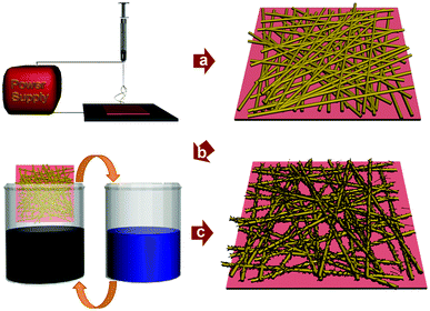 | ||
| Fig. 1 Fabrication process of the SWCNT/PU nanoweb to produce a transparent, elastic conductor. | ||
We used pristine SWCNTs to create a dipping solution; however, some of the CNTs were absorbed onto the surface of the PU nanofibers, but others were located in undesirable positions, such as voids in the nanowebs (Fig. S3†), thus preventing optimal application of the electrospun film. Therefore, we introduced additional functional groups, such as hydroxyl and carboxyl groups, into the SWCNTs via an acid treatment because those functionalities can form strong hydrogen bonds with the urethane groups in the PU nanofibers.30–32 The formation of hydroxyl and carboxyl groups in acid-treated SWCNTs (a-SWCNT) was confirmed by FT-IR (Fig. S4a†) and XPS (Fig. S4b†). It was also demonstrated by Raman spectroscopy. Fig. S4c (ESI†) shows the Raman spectra of pristine and a-SWCNTs which were normalized to the G-band peak. Compared with the D-band of untreated SWCNTs (ID/IG = 0.012), that of a-SWCNTs (ID/IG = 0.12) was increased, suggesting the formation of defects and less crystalline graphitic structures due to functionalization.33,34 Also, the slight change of the G-band from 1594 to 1596 cm−1 indicates the chemical charge-transfer on oxidized SWCNTs. The existence of radial breathing modes (RBM) in the Raman spectra shows that a-SWCNTs remained their tubular structure and tube diameters were not significantly altered after functionalization.35 The degree of carboxylation of SWCNTs was evaluated by TGA. As shown in Fig. S4d†, the weight loss difference between SWCNTs and a-SWCNTs corresponds to the presence of one carboxyl group per twenty-three carbon atoms of SWCNTs.36 Then, an a-SWCNT dipping solution was created; most a-SWCNTs were self-assembled on the surfaces of the PU nanofibers (see experimental section for details).
The amount of a-SWCNTs adsorbed onto the nanoweb could be controlled by the number of dipping cycles. We increased the dipping time to more than 1 min, but it did not affect the a-SWCNT coverage on the PU nanofibers. Fig. 2 shows the dependence of the morphological changes on the dipping-and-washing cycles. Between the first and fifth dipping-and-washing cycles, the nanofibers were not entirely covered by the a-SWCNTs, and some regions still remained uncovered. After the fifth cycle, the PU nanoweb structure was completely coated with a-SWCNTs. More dipping-and-washing cycles slightly increased the number of adsorbed a-SWCNTs, but the effect was low. This trend can also be confirmed by the changes in the sheet resistance with the number of dipping cycles (Fig. 3a). Until the 5th dipping cycle, the change in the sheet resistance of these composites was significantly reduced as the number of dipping-and-washing cycles increased. After that, their sheet resistance values still show a declining tendency as more dipping-and-washing cycles were applied but do not change greatly. The electrospinning time also acts as a variable that affects the conducting behavior of the composites. Samples electrospun for 30 s exhibit poor conducting behavior compared to other samples, indicating polyurethane nanofibers and adsorbed a-SWCNTs can not form well-connected conducting networks. However, for excessively long electrospinning times, such as 10 min, the sheet resistance of the samples was higher than that of the other samples after the same number of dipping cycles because the large thickness of the PU films effectively prevented the a-SWCNTs from adsorbing onto the surfaces of the nanofibers.
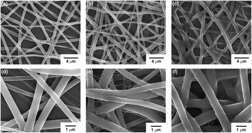 | ||
| Fig. 2 SEM images of the a-SWCNT/PU nanoweb after the 1st (a, d), 5th (b, e), and 9th (c, f) dipping cycles. | ||
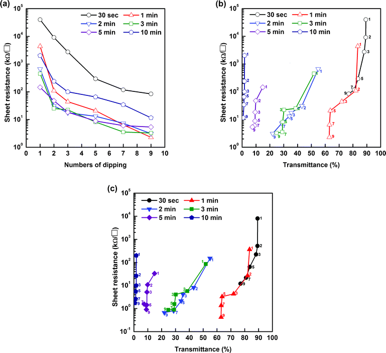 | ||
| Fig. 3 (a) Sheet resistance of a-SWCNT/PU nanoweb after different electrospinning times as a function of the number of dipping cycles. (b) Plot of sheet resistance vs. transmittance before doping and (c) after doping. The number on the symbol denotes the number of dipping cycles. | ||
The transmittance of the a-SWCNT/PU nanoweb conductor at 550 nm was evaluated by UV-vis spectroscopy; the transmittance is greatly affected by both the electrospinning time and the number of dipping cycles. Fig. S5 (ESI†) shows photographs of the samples and the variation in transmittance with the number of dipping cycles for each sample. Additionally, we plotted the sheet resistance of the conductors as a function of transmittance (at 550 nm) in Fig. 3b. Electrospinning for more than 2 min significantly reduced the transmittance of the films, while the samples that were electrospun for 2 and 3 min, respectively, showed resistances similar to those that were electrospun for 1 min. Thus, it can be concluded that a well-connected PU network is already formed after 1 min of electrospinning, which can allow maximum sample conductivity.
To improve their conductivity, we chemically doped the samples by dipping them into AuCl3 solution. In general, chemical p-type doping results from the formation of a charge-transfer complex between the SWCNTs and Lewis acids, such as nitric acid, AuCl3, and SOCl3.37,38 In this case, gold ions (Au3+) extract electrons from CNTs and turn them into a reduced form of Au0. The reduction of Au3+ ions can be revealed by XPS analysis: doublets assigned to Au0 located between 84.0 and 87.9 eV increased in intensity, while the two peaks associated with Au3+ between 86.6 and 90.3 eV were greatly diminished (Fig. S6a†). Also, a 0.2 eV shift of the C1s core level indicates a Fermi level shift induced by charge transfer (Fig. S6b†) after doping.37 We can observe gold clusters, which formed on the surfaces of the CNTs, through reflected-electron (COMPO) images of doped a-SWCNT/PU conductors (Fig. S6c†). The doping process does not affect the transmittance but reduces the sheet resistance by 90% compared with that of the undoped conductors, as shown in Fig. 3c. Our best sample exhibited a sheet resistance of 424 Ω sq−1 at 63%T. To compare the performance of transparent conducting films, the ratio of the direct current conductivity (σdc) to the optical conductivity (σac) is used as a figure of merit (FOM). A high value of σdc/σac indicates a material with a high conductivity and a low optical absorption and thus a superior candidate for transparent electrodes. For thin conducting films, this FOM can be calculated from the following relationship:
 | (1) |
The electrical conductivity of the composite films and reversibility of the stretch–release cycles were measured under tensile strains ranging from 0 to 100%. The films were uniaxially stretched using a mechanical stretching system with precise length control (Fig. 4a). At each applied strain, current–voltage curves were recorded and showed linear behavior, indicating good ohmic contacts between the films and electrodes.17 During the first cycle of stretching, the resistance of the a-SWCNT/PU film gradually increased as the tensile strain increased. This is because stretching leads to less interconnection or decreased contact area between neighboring a-SWCNTs attached on the nanofibers.43 When the films were stretched to 100%, the resistance increased by a factor of 4.4 (from 4.24 to 18.7 kΩ, Fig. 4b). Upon releasing the sample from tensile strain, the conductivity of the pre-stretched composite was slightly recovered. We then performed the second cycle of stretching up to 100%. The change in resistance during the second cycle was half of that during the first cycle. Interestingly, the variation in resistance under tensile strain was steadily reduced when more stretching/releasing cycles were applied. To understand this behavior, we observed the morphological changes under various strains. As shown in Fig. S7†, PU nanofibers are extended along the direction of tension during stretching. After the applied strain is removed, the elongated fibers cannot recover their original shape but turn into wavy and noodle-like structures. While the connections between some of the CNTs are broken or locally detached due to the excessive stretching, some of them are recovered during the releasing process, which contributes to the reduced resistance when they are fully released. When the film is stretched again, the greatest change observed is the straightening of the wavy PU nanofibers such that the overall resistance does not change significantly, unlike after the first stretching cycle.44
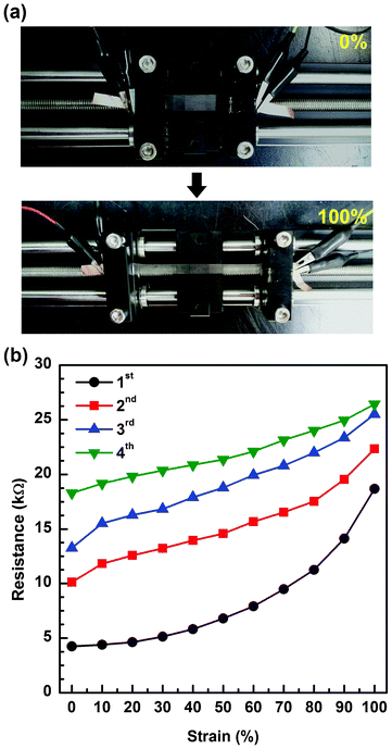 | ||
| Fig. 4 (a) Images of a-SWCNT/PU conductor under tensile strain of 0 and 100%. (b) Resistance of the a-SWCNT/PU conductor as a function of tensile strain over multiple stretching cycles. | ||
Even though our samples obtain their equilibrium resistance value after a number of stretch–release cycles, this cycling is an inefficient and time-consuming process because the samples have to be pretreated (stretched and released several times) before being incorporated into other compliant devices. Based on the permanent morphological changes observed during the first stretch–release cycle, we adjusted the experimental method as shown in Fig. 5. First, we placed a 3M VHB film on a PU electrospun Cu foil. Due to its sticky nature, the PU nanoweb could be transferred to the 3M VHB film, and the Cu foil was easily stripped off. The reason for this substrate-substituting process is that a PU nanoweb without a substrate curls up easily and is difficult to handle. Additionally, unlike the Cu foil, the 3M VHB film, which is a transparent elastomer, has a large elastic range. Then, the PU nanoweb on the 3M VHB film was uniaxially stretched and submitted to a dipping-and-washing cycle. Finally, it was dipped into the doping solution and released to its original length. The large difference in the elastic range between the PU elastomer and 3M VHB film leads to a more-sophisticated instant noodle-like structure, buckled and coiled, as shown in Fig. 6a. After the pre-stretching process, we measured the variation in resistance of these conductors over several stretch–release cycles. During the first cycle of stretching to 100%, the resistance of the pre-stretched sample increased by a factor of 1.3, which is much less than that of the pristine sample. The releasing process can slightly recover the resistance. The change in resistance became smaller as repetitive stretch–release cycles were applied, but the equilibrium resistance value was obtained more quickly than for the untreated sample (Fig. 6b). The variation in resistance during each stretching/releasing cycle was also recorded to determine the reversibility, as shown in Fig. 6c. A stable resistance was attained after more than six stretch–release cycles. Thus, the resistances under tensile strain in the range of 0 to 100% remained almost stable at an average value of 8.15 kΩ.
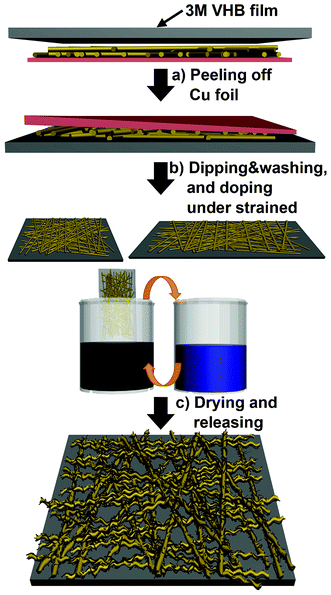 | ||
| Fig. 5 Schematic illustration of the procedure used to pre-strain the a-SWCNT/PU conductor. | ||
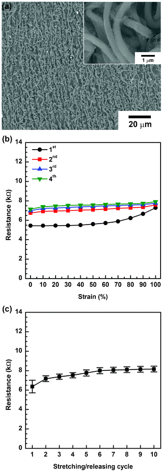 | ||
| Fig. 6 (a) SEM images of pre-strained a-SWCNT/PU conductor, (inset) magnified image. (b) Resistance of the pre-strained a-SWCNT/PU conductor as a function of tensile strain during each stretching cycle. (c) The stability of the resistance under multiple stretch–release cycles. Error bars indicate the minimum and maximum values of resistance while stretching. | ||
Conclusions
We fabricated net-shaped PU coated with a-SWCNTs using an electrospinning and dipping process, which can be used as a transparent and elastic conductor. Electrospun elastic scaffolds enable a-SWCNTs to form a percolated structure even at a low concentration, such that a highly transparent conductor can be obtained. Additionally, dipping the conductors in AuCl3 solution can further increase the conductivity by hole-doping of the SWCNTs. These samples show stable resistance after several stretch–release cycles are applied. When we first stretch the electrospun PU film and perform the dipping-and-washing cycles, followed by doping, those pre-strained conductors exhibit stable electrical characteristics under 100% strain. Our results demonstrate an effective way of preparing a transparent and elastic conductor that exhibits stable performance during excessive stretching.Acknowledgements
This work was financially supported by the Photo-electronic Hybrids Research Center of the Korea Institute of Science and Technology (KIST). Also, this work was supported by a grant (Code No. 2011-0032156) from the Center for Advanced Soft Electronics under the Global Frontier Research Program of the Ministry of Education, Science and Technology, Korea.References
- H. X. Chang, G. F. Wang, A. Yang, X. M. Tao, X. Q. Liu, Y. D. Shen and Z. J. Zheng, Adv. Funct. Mater., 2010, 20, 2893–2902 CrossRef CAS.
- Z. G. Wang, Y. F. Chen, P. J. Li, X. Hao, J. B. Liu, R. Huang and Y. R. Li, ACS Nano, 2011, 5, 7149–7154 CrossRef CAS.
- S. C. B. Mannsfeld, B. C. K. Tee, R. M. Stoltenberg, C. V. H. H. Chen, S. Barman, B. V. O. Muir, A. N. Sokolov, C. Reese and Z. N. Bao, Nat. Mater., 2010, 9, 859–864 CrossRef CAS.
- T. Someya, Y. Kato, T. Sekitani, S. Iba, Y. Noguchi, Y. Murase, H. Kawaguchi and T. Sakurai, Proc. Natl. Acad. Sci. U. S. A., 2005, 102, 12321–12325 CrossRef CAS.
- H. C. Ko, M. P. Stoykovich, J. Z. Song, V. Malyarchuk, W. M. Choi, C. J. Yu, J. B. Geddes, J. L. Xiao, S. D. Wang, Y. G. Huang and J. A. Rogers, Nature, 2008, 454, 748–753 CrossRef CAS.
- R. H. Kim, D. H. Kim, J. L. Xiao, B. H. Kim, S. I. Park, B. Panilaitis, R. Ghaffari, J. M. Yao, M. Li, Z. J. Liu, V. Malyarchuk, D. G. Kim, A. P. Le, R. G. Nuzzo, D. L. Kaplan, F. G. Omenetto, Y. G. Huang, Z. Kang and J. A. Rogers, Nat. Mater., 2010, 9, 929–937 CrossRef CAS.
- B. J. Hansen, Y. Liu, R. S. Yang and Z. L. Wang, ACS Nano, 2010, 4, 3647–3652 CrossRef CAS.
- D. Khodagholy, T. Doublet, M. Gurfinkel, P. Quilichini, E. Ismailova, P. Leleux, T. Herve, S. Sanaur, C. Bernard and G. G. Malliaras, Adv. Mater., 2011, 23, H268 CrossRef CAS.
- D. H. Kim, J. L. Xiao, J. Z. Song, Y. G. Huang and J. A. Rogers, Adv. Mater., 2010, 22, 2108–2124 CrossRef CAS.
- F. Xu, W. Lu and Y. Zhu, ACS Nano, 2011, 5, 672–678 Search PubMed.
- S. Kim, H. Y. Jeong, S. K. Kim, S. Y. Choi and K. J. Lee, Nano Lett., 2011, 11, 5438–5442 CrossRef CAS.
- T. Sekitani and T. Someya, Adv. Mater., 2010, 22, 2228–2246 CrossRef CAS.
- L. B. Hu, W. Yuan, P. Brochu, G. Gruner and Q. B. Pei, Appl. Phys. Lett., 2009, 94.
- T. Sekitani, H. Nakajima, H. Maeda, T. Fukushima, T. Aida, K. Hata and T. Someya, Nat. Mater., 2009, 8, 494–499 CrossRef CAS.
- T. Sekitani, Y. Noguchi, K. Hata, T. Fukushima, T. Aida and T. Someya, Science, 2008, 321, 1468–1472 CrossRef CAS.
- K. Y. Chun, Y. Oh, J. Rho, J. H. Ahn, Y. J. Kim, H. R. Choi and S. Baik, Nat. Nanotechnol., 2010, 5, 853–857 CrossRef CAS.
- Y. Y. Zhang, C. J. Sheehan, J. Y. Zhai, G. F. Zou, H. M. Luo, J. Xiong, Y. T. Zhu and Q. X. Jia, Adv. Mater., 2010, 22, 3027–3031 CrossRef CAS.
- H. Wu, L. B. Hu, M. W. Rowell, D. S. Kong, J. J. Cha, J. R. McDonough, J. Zhu, Y. A. Yang, M. D. McGehee and Y. Cui, Nano Lett., 2010, 10, 4242–4248 CrossRef CAS.
- K. D. Behler, A. Stravato, V. Mochalin, G. Korneva, G. Yushin and Y. Gogotsi, ACS Nano, 2009, 3, 363–369 CrossRef CAS.
- M. Havel, K. Behler, G. Korneva and Y. Gogotsi, Adv. Funct. Mater., 2008, 18, 2322–2327 CrossRef CAS.
- B. Chandra, A. Afzali, N. Khare, M. M. El-Ashry and G. S. Tulevski, Chem. Mater., 2010, 22, 5179–5183 CrossRef CAS.
- K. K. Kim, S. M. Yoon, H. K. Park, H. J. Shin, S. M. Kim, J. J. Bae, Y. Cui, J. M. Kim, J. Y. Choi and Y. H. Lee, New J. Chem., 2010, 34, 2183–2188 RSC.
- C. J. Yu, C. Masarapu, J. P. Rong, B. Q. Wei and H. Q. Jiang, Adv. Mater., 2009, 21, 4793 CrossRef CAS.
- X. Feng, B. D. Yang, Y. M. Liu, Y. Wang, C. Dagdeviren, Z. J. Liu, A. Carlson, J. Y. Li, Y. G. Huang and J. A. Rogers, ACS Nano, 2011, 5, 3326–3332 Search PubMed.
- J. Lee, J. A. Wu, M. X. Shi, J. Yoon, S. I. Park, M. Li, Z. J. Liu, Y. G. Huang and J. A. Rogers, Adv. Mater., 2011, 23, 986–991 CrossRef CAS.
- B. Carlberg, M. Z. Axell, U. Nannmark, J. Liu and H. G. Kuhn, Biomed. Mater., 2009, 4 Search PubMed.
- M. S. Khil, D. I. Cha, H. Y. Kim, I. S. Kim and N. Bhattarai, J. Biomed. Mater. Res., 2003, 67B, 675–679 Search PubMed.
- C. A. Hunter and J. K. M. Sanders, J. Am. Chem. Soc., 1990, 112, 5525–5534 CrossRef CAS.
- S. S. Tallury and M. A. Pasquinelli, J. Phys. Chem. B, 2010, 114, 9349–9355 CrossRef CAS.
- H. S. Kim, H. J. Jin, S. J. Myung, M. S. Kang and I. J. Chin, Macromol. Rapid Commun., 2006, 27, 146–151 CrossRef CAS.
- Y. Xiao, S. B. Zhou, L. Wang and T. Gong, ACS Appl. Mater. Interfaces, 2010, 2, 3506–3514 Search PubMed.
- Y. C. Jung, H. H. Kim, Y. A. Kim, J. H. Kim, J. W. Cho, M. Endo and M. S. Dresselhaus, Macromolecules, 2010, 43, 6106–6112 CrossRef CAS.
- C. Lu and H. Chiu, Chem. Eng. J., 2008, 139, 462–468 Search PubMed.
- H. Yu, Y. G. Jin, Z. L. Li, F. Peng and H. J. Wang, J. Solid State Chem., 2008, 181, 432–438 CrossRef CAS.
- Y. Kim, D. Lee, Y. Oh, J. Choi and S. Baik, Synth. Met., 2006, 156, 999–1003 CrossRef CAS.
- Y. J. Song, J. U. Lee and W. H. Jo, Carbon, 2010, 48, 389–395 CrossRef CAS.
- T. A. Kim, H. S. Kim, S. S. Lee and M. Park, Carbon, 2012, 50, 444–449 Search PubMed.
- S. M. Kim, K. K. Kim, Y. W. Jo, M. H. Park, S. J. Chae, D. L. Duong, C. W. Yang, J. Kong and Y. H. Lee, ACS Nano, 2011, 5, 1236–1242 Search PubMed.
- J. W. Jo, J. W. Jung, J. U. Lee and W. H. Jo, ACS Nano, 2010, 4, 5382–5388 CrossRef CAS.
- B. Dan, G. C. Irvin and M. Pasquali, ACS Nano, 2009, 3, 835–843 CrossRef CAS.
- M. S. Jung, T. L. Choi, W. J. Joo, J. Y. Kim, I. T. Han and J. M. Kim, Synth. Met., 2007, 157, 997–1003 Search PubMed.
- P. J. King, T. M. Higgins, S. De, N. Nicoloso and J. N. Coleman, ACS Nano, 2012, 6, 1732–1741 Search PubMed.
- Q. W. Li, Y. Li, X. F. Zhang, S. B. Chikkannanavar, Y. H. Zhao, A. M. Dangelewicz, L. X. Zheng, S. K. Doorn, Q. X. Jia, D. E. Peterson, P. N. Arendt and Y. T. Zhu, Adv. Mater., 2007, 19, 3358 CrossRef CAS.
- F. Xu and Y. Zhu, Adv. Mater., 2012, 24, 5117 Search PubMed.
Footnote |
| † Electronic Supplementary Information (ESI) available: See DOI: 10.1039/c2ra20792c |
| This journal is © The Royal Society of Chemistry 2012 |