Energy-transfer luminescence of a zinc oxide/ytterbium oxide nanocomposite
Mikhail V.
Shestakov
ab,
Andrey N.
Baranov
*c,
Victor K.
Tikhomirov
b,
Yan V.
Zubavichus
d,
Alexander S.
Kuznetsov
b,
Alexey A.
Veligzhanin
d,
Alexander Yu.
Kharin
a,
Roland
Rösslhuber
e,
Victor Yu.
Timoshenko
e and
Victor V.
Moshchalkov
b
aDepartment of Materials Science, Lomonosov Moscow State University, Moscow, Russia
bINPAC – Institute for Nanoscale Physics and Chemistry, KU Leuven, Belgium
cDepartment of Chemistry, Lomonosov Moscow State University, Moscow, Russia. E-mail: anb@inorg.chem.msu.ru
dNational Research Centre “Kurchatov Institute”, Moscow, Russia
eDepartment of Physics, Lomonosov Moscow State University, Moscow, Russia
First published on 25th July 2012
Abstract
A newly structured nanocomposite material based on nanocrystalline ZnO/Yb2O3 has been prepared by thermal decomposition of Yb-doped zinc carbonate hydroxide. Transmission electron microscopy has revealed that the prepared nanopowder consists of ZnO nanocrystals of about 50 to 100 nm size decorated by attached smaller Yb2O3 nanocrystals of about 10 to 15 nm size. X-Ray absorption spectroscopy, in particular XANES and EXAFS, indicate the charge of Yb ions equals to +3 and their coordination is oxygen octahedral with the Yb–O and Yb–Yb interatomic distances the same as in bulk Yb2O3. Photoluminescence spectroscopy unambiguously proves an efficient excitation energy transfer from the ZnO nanocrystals to the Yb3+ ions. The energy transfer from the ZnO nanocrystals (absorption range from 250 to 400 nm) to the Yb3+ ions (emission range from 950 to 1100 nm) has been explained by a model, which considers the quantum cutting effect. The prepared nanocomposite is promising for application as a down-conversion layer for enhanced solar cells.
Introduction
Zinc oxide (ZnO) nanostructures are very promising candidates for numerous electronic and optoelectronic applications. They find applications in gas sensors,1 transparent conductive electrodes,2 electrodes for water-splitting/hydrolysis,3 sun screens,4 UV-lasers,5 light emitting diodes,6 luminescent species for down-conversion layers,7,8 organic/hybrid solar cells,9 piezotronics and piezo-phototronics.10ZnO is a direct wide-gap semiconductor with strong absorption bands in the UV and blue ranges due to the band–band and excitons-related optical transitions and high transparency in the visible and near infrared ranges.11,12 Furthermore, its properties can be purposely tuned by doping with various elements.7,13–15 At present, there are several different methods and techniques for synthesis of ZnO nanostructures, e.g. chemical vapor deposition,16 solution methods,17,18 hydrothermal methods19,20 and growth from salt mixtures.21,22
In this work, a method for the preparation of ZnO:Yb nanopowder has been proposed, newly structured ZnO/Yb2O3 nanocomposite has been synthesized and the structural and optical properties of this material have been investigated. We have detected the luminescence band of Yb3+ at about 1000 nm, which was excited by energy transfer from the optically pumped ZnO nanoparticles. The pump power dependence and temperature dependence of this Yb3+ emission band indicate that a combination of the quantum cutting (sub-linear) and a minor admixture of linear intensity dependence mechanisms are involved in the energy transfer from ZnO to Yb3+ ions. Hence, a mechanism for the excitation of the Yb3+ emission band has been proposed and shown to occur mostly by quantum cutting, i.e. by generation of two photons emitted by the Yb3+ dopant due to the absorption of one photon by ZnO nanocrystals.
The nanocomposite ZnO/Yb2O3 is proposed for use in down-conversion layers for enhanced solar cells by encapsulating this nanopowder in polymer film anti-reflectors on a solar cell.
Experimental section
Zinc oxide, ytterbium nitrate pentahydrate salt, nitric acid and ammonium hydrocarbonate were purchased from commercial providers, like Alfa Aesar, and used without purification. Zinc oxide was dissolved in nitric acid (10 mol%). Ytterbium nitrate pentahydrate salt was added to the solution. Several samples with molar ratios of Yb to Zn cations from 0 to 0.01 were prepared. Zinc hydroxocarbonate (ZCH) was precipitated by NH4HCO3 aqueous solution, while the molar ratio of carbonate to zinc ions was equal to 4. The precipitated ZCH, which contained homogeneously dispersed Yb precursor, was washed with distilled water and freeze-dried in a laboratory freeze dryer. The dried powder was annealed in a muffle furnace at 700 °C during 1 h.The nanoparticles' structure/morphology was studied by means of transmission electron microscopy (TEM) using a LEO912 AB OMEGA microscope operated at 100 keV. X-Ray diffraction measurements (XRD) were carried out using a Rigaku D/MAX 2500 diffractometer (Cu-Kα radiation). Yb L3-edge X-ray absorption/fluorescence spectroscopy (XAS) measurements were done in the fluorescence mode at the synchrotron radiation facility “Siberia-2”, Kurchatov Synchrotron Radiation Source, Moscow, using a Si(111) channel-cut monochromator, an ionization chamber as a beam intensity monitor and an avalanche photodiode as an X-ray fluorescence detector. The respective measurement techniques and set ups were described elsewhere.23 Extended X-ray Absorption Fine Structure spectra (EXAFS) processing and analysis were carried out using the IFEFFIT code with FEFF photoelectron scattering amplitude and phase functions.24,25 The non-linear fitting of the oscillatory parts of EXAFS spectra was done over the range of wave vector, k, from 3 to 12 Å−1 and interatomic distance range, r, from 1.4 to 4.3 Å using a Hanning window function. The following parameters were fitted: energy origin shift (Eo), interatomic distances for the two nearest coordination spheres Yb–O and Yb–Yb, and the Debye–Waller factor (σ2). The coordination numbers for these spheres were fixed at the crystallographic values typical of Yb2O3.
For optical measurements the nanopowders have been pressed in pellets. The excitation and photoluminescence (PL) spectra have been measured using an Andor Technologies Newton DU970 EMCCD camera attached to a Shamrock SR303i spectrometer sensitive in the range from 400 to 1100 nm. A Solar LS grating spectrometer equipped by a CCD-unit was used for the PL measurements in the range from 400 to 1500 nm. PL excitation spectra have been detected using a tunable Xe lamp (300 W) source. An Ar+ laser operating at 355 and 364 nm monochromatic lines with a power up to 60 mW was used for measurements of the dependence of PL intensity on excitation intensity by attenuating the latter with a set of neutral filters. The temperature dependence of PL intensity was detected when cooling down the samples in a He flow cryostat. Spectral responses of the detection systems have been taken into account.
Results
TEM studies revealed that the ZnO:Yb nanocomposite powder consists of relatively large 50–100 nm ZnO crystalline nanoparticles with attached Yb2O3 crystalline nanoparticles with a size of 10–15 nm, as seen in Fig. 1(a). Fig. 1(b) shows the selected area electron diffraction (SAED) pattern of the nanocomposite. The individual diffraction spots in (b) can be identified as reflexes of the ZnO nanoparticles, whereas the diffraction circles in (b) can be attributed to substantially smaller Yb2O3 nanoparticles.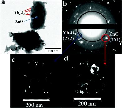 | ||
| Fig. 1 (a) TEM images of ZnO/Yb2O3 nanocomposite powder, i.e. of ZnO crystalline nanoparticles decorated with attached smaller Yb2O3 crystalline nanoparticles; (b) selected area electron diffraction (SAED) pattern of the area shown in (a); (c,d) dark-field images of the areas circled and arrowed by the blue and red circles and arrows in (b), respectively. | ||
Fig. 1(a) in our manuscript shows that Yb2O3 nanoparticles locate at the surface of ZnO nanoparticles. This is a typical and representative picture for our samples. We did not find that Yb2O3 nanoparticles incorporate inside ZnO nanoparticles by closer inspection of larger areas/volumes within our samples. The Yb2O3 inclusions within ZnO nanoparticles could be seen in TEM images of ZnO nanoparticles of small thickness of less than 100 nm; but we have not detected the Yb2O3 phase inside of even thinner ZnO nanoparticles.
By switching from the diffraction to imaging mode we got dark-field images of the nanoparticles responsible for the diffraction. The fragments of the SAED are depicted in Fig. 1(c,d), the dark-field images correspond to the areas highlighted by blue and red circles in Fig. 1b, respectively. In the case presented by the blue circle, Fig. 1(c), we observe the scattering of electrons from only the Yb2O3 nanoparticles and these nanoparticles are visualized. In the case presented by the red circle, Fig. 1(d), we observe both Yb2O3 and ZnO nanoparticles contributions and the dark-field image is formed by small Yb2O3 and large ZnO nanoparticles, respectively.
The ZnO and ZnO:Yb nanopowders were also studied by means of XRD; an example is shown in Fig. 2. In both doped and undoped nanopowders, all diffraction peaks are well indexed as Zincite (JCPDC card 36-1451). For the ZnO:Yb nanopowders, an extra low intense peak is also seen; it corresponds to the most intense reflex (222) of the crystalline Yb2O3 phase. None other reflexes and/or therefore none respective impurities phases were detected. The lattice cell parameters of the undoped ZnO (a = 3.2506(2) Å; c = 5.2078(3) Å) are found to be similar to the parameters of the Yb-doped ZnO (a = 3.2493(5) Å; c = 5.2061(1) Å).
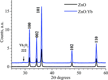 | ||
| Fig. 2 XRD patterns of undoped and Yb-doped ZnO nanopowders (1 mol% doping). The Miller indices of the würtzite ZnO crystalline phase are labeled, respectively. One of the highest intensity reflexes of the Yb2O3 phase, the (222), is arrowed. | ||
The spectra of X-ray Absorption Near Edge Structure (XANES) of the Yb L3-edge of the ZnO:Yb nanocomposite are shown in Fig. 3. For comparison, the spectra of standard references of Yb2O3 and YbAl2 are also shown in Fig. 3. YbAl2 is a well-known standard with the homogeneous mixed-valence state of ytterbium ions with an effective valence of 2.25–2.30.26,27 As it becomes evident from Fig. 3, EXAFS and XANES spectra of Yb2O3 standard and ZnO:Yb nanocomposite powder show very similar shape. Therefore, it can be concluded that the oxidation state and coordination environment of Yb ions are very similar in our ZnO:Yb nanocomposites and crystalline Yb2O3 standard reference. None trace of the Yb2+ was detected in our ZnO:Yb nanopowders, since the XANES signal from the Yb2+ valence state is 7 eV below the signal from the Yb3+ state, as can be seen in Fig. 3 and in Ref. 26,27, and the Yb2+ signal does not contribute to the spectrum of our ZnO:Yb nanopowders.
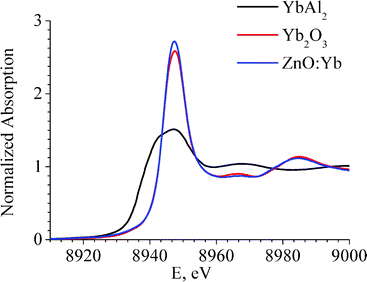 | ||
| Fig. 3 Yb L3-edge XANES spectra of the ZnO:Yb nanocomposite powder (doping level 1 mol%, blue curve), and of the Yb2O3 standard (red curve) and YbAl2 standard (black curve) references. | ||
The results of the fitting procedure for EXAFS spectra are shown in Fig. 4 and listed in Table 1. The matching of the EXAFS and best-fit local structure parameters between the ZnO:Yb nanopowder and Yb2O3 standard reference indicate that Yb3+ ions in the Yb-doped ZnO nanopowder are dispersed in the Yb2O3 phase. A minor difference between the ZnO:Yb nanopowder and Yb2O3 standard, which can be seen in Table 1 may be related to nano-scale size of the Yb2O3 nanoparticles and/or slight structural distortions of the Yb2O3 nanoparticles at the interface with the ZnO nanoparticles.29
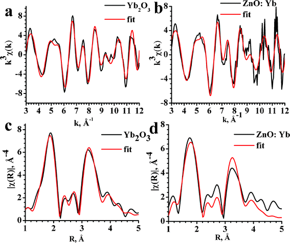 | ||
| Fig. 4 Oscillatory parts and Fourier transforms of Yb L3-edge EXAFS spectra for Yb2O3 (a,c) and ZnO:Yb (b,d) nanopowders. Experimental data are presented by black lines and the best fits by the red lines. | ||
| Yb–O | Yb–Yb1 | Yb–Yb2 | |
|---|---|---|---|
| Yb2O3 | 2.23 (2.21–2.28) | 3.46 (3.46–3.48) | 3.93 (3.93–3.95) |
| ZnO:Yb | 2.21 | 3.47 | 3.94 |
Fig. 5(a,b) show PL excitation and emission spectra of undoped ZnO and ZnO:Yb nanopowders. The PL spectrum of undoped ZnO shows only one broad emission band with a maximum in the green at about 550 nm, which is the normal “intrinsic” emission band of ZnO, which is related to oxygen vacancies, e.g. in Ref. 11,12,31,32 and references therein. The PL spectrum of the Yb doped nanopowder shows an extra emission band at about 1000 nm, typical of the Yb3+ dopants, e.g. in Ref. 7,8,14,30 and references therein. Therefore we ascribe this band to the Yb3+ dopant, noting that this band is even stronger than the green PL band of the ZnO host. The excitation spectra for the green PL (detected at 550 nm) and for the Yb3+ (detected at 980 nm) emission bands are shown in Fig. 5(b).
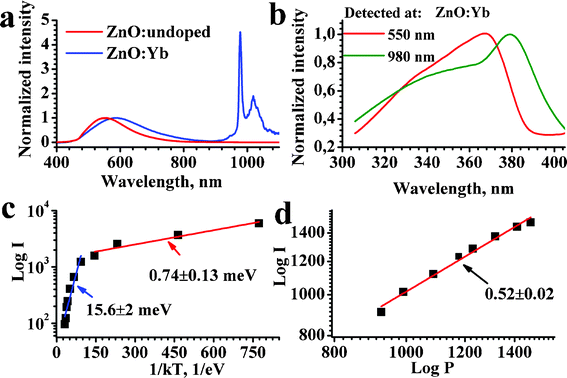 | ||
| Fig. 5 (a) Normalized PL spectra of undoped (red curve) and Yb3+-doped (blue curve) ZnO nanopowder excited at 355 nm; (b) normalized excitation spectra of the intrinsic (red curve) and Yb3+ (green curve) PL bands of ZnO:Yb nanopowder; (c) temperature dependence of the Yb3+ emission band of ZnO:Yb nanopowder excited at 364 nm; (d) room temperature pump power dependence of the Yb3+ PL band excited at 364 nm. The excitation and detection conditions, and the slopes are labeled, respectively; the Yb3+ doping level was 1 mol%. | ||
The excitation maximum at about 380 nm, Fig. 5(b), in the Yb-doped sample can be attributed to the excitation of Yb3+via an exciton state of the ZnO host, because it exactly corresponds to the exciton absorption band of ZnO (Ref. 11,12 and references therein). A weaker shoulder at shorter excitation wavelengths can be related to the direct excitation of Yb3+ from the conduction band of ZnO and also to the charge transfer from d-states of Yb3+ (Ref. 14,33 and references therein). Thus, the main excitation mechanism for the Yb3+ emission is due to the energy transfer from exciton state of the ZnO host; this conclusion is in agreement with results of Ref. 7,14. On the other hand, as represented by the red curve in Fig. 5(b), the green intrinsic PL band of ZnO occurs only by energy transfer from the conduction band of ZnO by thermal relaxation of the excited carriers to the oxygen vacancies with subsequent emission from these deep vacancies. The mechanism for the intrinsic green emission band of ZnO is known from the literature, e.g. in Ref. 7,11,31,32 and references therein. The mechanisms for the intrinsic ZnO and Yb3+ dopants luminescence are depicted schematically in the energy level diagram of Fig. 6.
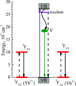 | ||
| Fig. 6 Energy level diagram illustrating the energy transfer processes by quantum cutting from the ZnO exciton state to a pair of Yb3+ ions nearby. The purple solid up-headed arrow shows excitation of electrons from the valence (VB) to the conduction band (CB) of ZnO. The violet horizontal line shows the exciton energy level of ZnO. A wavy black line shows trapping of electrons from the conduction band of zinc oxide by its intrinsic defects (oxygen vacancies) post-signed by the letter V, with subsequent emission of intrinsic green luminescence (green down-headed arrow). Red horizontal lines show the involved energy levels of Yb3+ ions and the black down-headed arrows indicate an experimentally detected emission of Yb3+ at about 1000 nm. The dashed black lines indicate energy transfer processes by quantum cutting from the ZnO exciton to the Yb3+ ions. | ||
Fig. 5(c,d) show the temperature dependence of the Yb3+ PL band and its intensity dependence at room temperature, respectively. The temperature dependence, when presented in Arrhenius coordinates, shows two different linear slopes at low and high temperature ranges, indicating two different energy transfer processes for the excitation of Yb3+ luminescence, as discussed further. The slope of about 0.5 in the intensity dependence shown in Fig. 5(d) indicates that the emission of Yb3+ occurs mostly by a quantum cutting mechanism, when one photon absorbed by the ZnO host initiates emission of two photons by Yb3+ dopants. The quantum cutting mechanism was predicted theoretically in Ref. 34.
Discussion
The obtained experimental results show that incorporation of Yb3+ ions within a ZnO crystalline host cannot be achieved. On the one hand, it agrees with the literature data, which demonstrated that different rare earth dopants cannot be dispersed within the ZnO crystalline phase and after annealing outdiffusion leads to the surface segregation of the rare earth ions implanted in the ZnO matrix.35–39 It is obviously related to differences in ionic radii and charging states of Zn2+ (0.88 Å) and Yb3+ (1.01 Å).40 On the other hand, we have found that incorporation of Yb3+ ions within a ZnO crystal lattice actually is not required for the efficient energy transfer ZnO→Yb3+ to take place. The latter can be realized when tiny Yb2O3 particles are attached to ZnO nanocrystals, while the nanoscale of the particle size is the principal aspect here as it ensures a larger surface/volume ratio and therefore larger surface contact between the ZnO and Yb2O3 nanoparticles. In fact, the nanocomposite ZnO/Yb2O3 powder prepared in this work ensures a tight contact and energy transfer between the ZnO and Yb2O3 nanophases.The proposed synthesis method results in the nanocomposite ZnO/Yb2O3 owing to a high homogenization of the precursor with high reactivity of the components at the synthesis temperature, which prevents growth of the Yb2O3 and ZnO phases as microscale aggregates and initiates a nanoscale reaction between Yb2O3 and ZnO. The freeze-drying technique was used in this work to eliminate the water from the precursor without allowing growth of the micro-phases.41
The diagram of the energy levels in Fig. 6 depicts the involved energy levels and optical transitions accounting for the presented PL data of Fig. 5. The pairs of Yb3+ ions should be close to each other to provide the necessary condition for efficient quantum cutting, i.e. for the simultaneous excitation of two Yb3+ ions by nonradiative decay of one exciton in ZnO. In this respect, the exciton Bohr radius of ZnO equals 14 Å;42 and then the pairs of Yb3+ ions can certainly be encompassed by an exciton of such radius. Here, it is very important to note that, in the Yb2O3 phase, interatomic distances between the Yb3+ ions are short (see Table 1), which essentially promotes the quantum cutting process by energy transfer from the exciton state. This explains the square root law of the PL intensity dependence on excitation power (see Fig. 5(d)), which is typical of the quantum cutting mechanism.7 Note the quantum cutting processes in Yb-doped and co-doped glasses and phosphors were reported in Ref. 43–45. A particular feature of the photon-cutting assisted energy transfer observed in our work is the involvement of intrinsic exciton states of the nanocrystalline ZnO matrix. A similar effect was recently detected for silicon nanocrystals in silicon dioxide matrix doped with Er.46
Based on the temperature dependence of Yb3+ PL (Fig. 5(c)) we conclude that two different quantum cutting mechanisms can be involved in the Yb3+ excitation. At high temperatures the PL intensity of Yb3+ depends more on temperature (the activation energy is about 16 meV), indicating a contribution of the Fröhlich mechanism to the involved electron–phonon interaction, when the lattice phonon initiates an interaction between the interacting dipoles in the donor (ZnO) and acceptor (Yb2O3) of energy.34 At low temperatures the PL intensity of the Yb3+ band varies weakly with temperature (the activation energy is about 0.7 meV), indicating the energy transfer is likely to be a tunneling process.
The prepared ZnO/Yb2O3 nanocomposite can be used in silicon photovoltaics, in particular, for down-conversion of the solar spectrum. The down-conversion is required in order to avoid a mismatch between the incident solar photon energy and the band gap of silicon, which is mostly employed in modern solar cells; the mismatch results in thermal losses of solar energy that degrade the solar cells, e.g. in Ref. 7,30,33,47. The well known Shockley–Queisser criterion says the maximum energy conversion efficiency (EQE) for conventional silicon solar cells is limited to 30%,48 but it has been recently suggested that the EQE value of silicon cells can be enhanced up to 40% by placing a thin down-conversion layer on the top of the cell,49 which converts the solar spectrum from UV-blue to longer wavelengths. Light-emitting ions of Yb3+ are especially promising for such down-conversion applications due to matching of the Yb3+ emission band, around 1000 nm, to the wavelength range of maximum light-to-current EQE of silicon solar cells.50–52
Conclusions
In this work, a new nanocomposite ZnO/Yb2O3 has been prepared by thermal decomposition of a mixed salt precursor. It is found that Yb3+ ions do not dissolve within the ZnO crystalline matrix but rather form Yb2O3 nanoparticles in a tight contact with larger ZnO nanoparticles, thus forming the nanocomposite. An efficient energy transfer from ZnO nanoparticles to Yb3+ ions has been detected, which occurs mostly by the quantum cutting mechanism. The nanocomposite ZnO/Yb2O3 can be proposed for use in down-conversion layers for enhanced solar cells by encapsulating this powder in polymer film anti-reflectors on solar cells, such as EVA and PMMA.Acknowledgements
We are grateful to the Methusalem Funding of the Flemish Government for support of this work. The synchrotron measurements at the Kurchatov centre were supported via the Russian federal contract 16.552.11.7003. The optical measurements were carried out using equipment of the Center of User's Facilities of Lomonosov Moscow State University. The work was partially supported by the Ministry of Education and Science of the Russian Federation (contract # 11.519.11.3017) and by the Russian Foundation for Basic Research (grants ## 11-02-01342, 11-02-90506 and 11-03-01124).References
- A. Wei, L. Pan and W. Huang, Mater. Sci. Eng., B, 2011, 176, 1409–1421 CrossRef CAS.
- C. Guillén and J. Herrero, Thin Solid Films, 2011, 520, 1–17 CrossRef.
- Y. Lin, G. Yuan, R. Liu, S. Zhou, S. W. Sheehan and D. Wang, Chem. Phys. Lett., 2011, 507, 209–215 CrossRef CAS.
- K. Schilling, B. Bradford, D. Castelli, E. Dufour, J. F. Nash, W. Pape, S. Schulte, I. Tooley, J. van den Bosch and F. Schellauf, Photochem. Photobiol. Sci., 2010, 9, 495–509 CAS.
- M. A. Zimmler, F. Capasso, S. Muller and C. Ronning, Semicond. Sci. Technol., 2010, 25, 024001 CrossRef.
- A. B. Djurišić, A. M. C. Ng and X. Y. Chen, Prog. Quantum Electron., 2010, 34, 191–259 CrossRef.
- M. V. Shestakov, V. K. Tikhomirov, D. Kirilenko, A. S. Kuznetsov, L. F. Chibotaru, A. N. Baranov, G. Van Tendeloo and V. V. Moshchalkov, Opt. Express, 2011, 19, 15955–64 CrossRef CAS.
- J. Zhou, Y. Teng, S. Ye, X. Liu and J. Qiu, Opt. Mater., 2010, 33, 153–158 CrossRef CAS.
- J. Huang, Z. G. Yin and Q. D. Zheng, Energy Environ. Sci., 2011, 4, 3861–3877 CAS.
- Z. L. Wang, Nano Today, 2010, 5, 540–552 CrossRef CAS.
- C. Klingshirn, Phys. Status Solidi B, 2007, 244, 3027–3073 CrossRef CAS.
- Ü. Özgür, Y. I. Alivov, C. Liu, A. Teke, M. A. Reshchikov, S. Doğan, V. Avrutin, S.-J. Cho and H. Morkoç, J. Appl. Phys., 2005, 98, 041301 CrossRef.
- W. M. Jadwisienczak, H. J. Lozykowski, A. Xu and B. Patel, J. Electron. Mater., 2002, 31, 776–784 CrossRef CAS.
- S. Ye, N. Jiang, F. He, X. Liu, B. Zhu, Yu Teng and J. Qiu, Opt. Express, 2010, 18, 639–644 CrossRef CAS.
- M. D. Mccluskey and S. J. Jokela, J. Appl. Phys., 2009, 106, 071101 CrossRef.
- J. Liu, W. Wu, S. Bai and Y. Qin, ACS Appl. Mater. Interfaces, 2011, 3, 4197–4200 CAS.
- L. Spanhel and M. Anderson, J. Am. Chem. Soc., 1991, 113, 2826–2833 CrossRef CAS.
- E. Meulenkamp, J. Phys. Chem. B, 1998, 102, 5566–5572 CrossRef CAS.
- J. Na, B. Gong, G. Scarel and G. N. Parsons, ACS Nano, 2009, 3, 3191–3199 CrossRef CAS.
- H. Zhang, D. Yang, Y. Ji, X. Ma, J. Xu and D. Que, J. Phys. Chem. B, 2004, 108, 3955–3958 CrossRef CAS.
- A. N. Baranov, G. N. Panin, T. W. Kang and Y.-J. Oh, Nanotechnology, 2005, 16, 1918–1923 CrossRef CAS.
- A. N. Baranov, C. H. Chang, O. A. Shlyakhtin, G. N. Panin, T. W. Kang and Y.-J. Oh, Nanotechnology, 2004, 15, 1613–1619 CrossRef CAS.
- A. A. Chernyshov, A. A. Velighzanin and Y. V. Zubavichus, Nucl. Instrum. Methods Phys. Res., Sect. A, 2009, 603, 95–98 CrossRef CAS.
- B. Ravel and M. Newville, J. Synchrotron Radiat., 2005, 12, 537–541 CrossRef CAS.
- S. I. Zabinsky, J. J. Rehr, A. Ankudinov, R. C. Albers and M. J. Eller, Phys. Rev. B: Condens. Matter, 1995, 52, 2995 CrossRef CAS.
- E. Beaurepaire, J. P. Kappler and G. Krill, Solid State Commun., 1986, 57, 145–149 CrossRef CAS.
- C. Dallera, E. Annese, J.-P. Rueff, A. Palenzona, G. Vankó, L. Braicovich, A. Shukla and M. Grioni, Phys. Rev. B: Condens. Matter, 2003, 68, 245114 CrossRef.
- H. Ishibashi, K. Shimomoto and K. Nakahigashi, J. Phys. Chem. Solids, 1994, 55, 809–814 CrossRef CAS.
- B. Jeyadevan, K. Tohji and K. Nakatsuka, J. Appl. Phys., 1994, 76, 6325 CrossRef CAS.
- V. D. Rodriguez, V. K. Tikhomirov, J. Mendez-Ramos, A. C. Yanes and V. V. Moshchalkov, Sol. Energy Mater. Sol. Cells, 2010, 94, 1612 CrossRef CAS.
- A. V. Dijken, E. A. Meulenkamp, D. Vanmaekelbergh and A. Meijerink, J. Lumin., 2000, 87-89, 454–456 CrossRef.
- A. V. Dijken, E. A. Meulenkamp, D. Vanmaekelbergh and A. Meijerink, J. Lumin., 2000, 90, 123–128 CrossRef.
- V. K. Tikhomirov, V. D. Rodríguez, A. S. Kuznetsov, D. Kirilenko, G. Van Tendeloo and V. V. Moshchalkov, Opt. Express, 2010, 18, 22032 CrossRef CAS.
- D. L. Dexter, Phys. Rev., 1957, 108, 630–633 CrossRef CAS.
- E. Rita, E. Alves, U. Wahl, G. Correia, T. Monteiro, M. Soares, A. Neves and M. Peres, Nucl. Instrum. Methods Phys. Res., Sect. B, 2006, 242, 580–584 CrossRef CAS.
- E. Alves, E. Rita, U. Wahl, G. Correia, T. Monteiro, M. Soares and C. Boemare, Nucl. Instrum. Methods Phys. Res., Sect. B, 2003, 206, 1047–1051 CrossRef CAS.
- T. Monteiro, M. J. Soares, A. Neves, M. Carmo, M. Peres, E. Alves, U. Wahl, E. Rita, V. Munoz-Sanjose and J. Zuniga-Perez, Phys. Status Solidi C, 2006, 3, 968–971 CrossRef CAS.
- S. M. C. Miranda, M. Peres, T. Monteiro, E. Alves, H. Sun, T. Geruschke, R. Vianden and K. Loren, Opt. Mater., 2011, 33, 1139–1142 CrossRef CAS.
- N. Jiang, S. Ye and J. Qiu, J. Appl. Phys., 2010, 108, 083535 CrossRef.
- B. K. Vainshtein, V. M. Fridkin and V. L. Indenbom, in Modern Crystallography 2: Structure of crystals, Nauka, Moscow; 2nd edn 1979, vol. 2, ch. 1, pp. 75-81 Search PubMed.
- Yu. D. Tretyakov and O. A. Shlyakhtin, J. Mater. Chem., 1999, 9, 19–24 RSC.
- T. Hirai, Y. Harada, S. Hashimoto, T. Itoh and N. Ohno, J. Lumin., 2005, 112, 196–199 CrossRef CAS.
- P. Vergeer, T. J. H. Vlugt, M. H. F. Kox, M. I. den Hertog, J. P. J. M. van der Eerden and A. Meijerink, Phys. Rev. B: Condens. Matter Mater. Phys., 2005, 71, 014119 CrossRef.
- H. Lin, S. Zhou, H. Teng, Y. Li, W. Li, X. Hou and T. Jia, J. Appl. Phys., 2010, 107, 043107 CrossRef.
- X. Wei, J. Zhao, W. Zhang, Y. Li and M. Yin, J. Rare Earths, 2010, 28, 166–170 CrossRef CAS.
- N. N. Ha, S. Cueff, K. Dohnalov, M. T. Trinh, C. Labbé, R. Rizk, I. N. Yassievich and T. Gregorkiewicz, Phys. Rev. B: Condens. Matter Mater. Phys., 2011, 84, 241308(R) CrossRef.
- B. S. Richards, Sol. Energy Mater. Sol. Cells, 2006, 90, 1189–1207 CrossRef CAS.
- W. Shockley and H. J. Queisser, J. Appl. Phys., 1961, 32, 510–519 CrossRef CAS.
- T. Trupke, M. A. Green and P. Wurfel, J. Appl. Phys., 2002, 92, 1668 CrossRef CAS.
- E. Klampaftis, D. Ross, K. R. McIntosh and B. S. Richards, Sol. Energy Mater. Sol. Cells, 2009, 93, 1182–1194 CrossRef CAS.
- Q. Luo, X. Qiao, X. Fan and X. Zhang, Opt. Lett., 2011, 36, 2767–2769 CrossRef CAS.
- I. Soumahoro, G. Schmerber, A. Douayar, S. Colis, M. Abd-Lefdil, N. Hassanain, A. Berrada, D. Muller, A. Slaoui, H. Rinnert and A. Dinia, J. Appl. Phys., 2011, 109, 033708 CrossRef.
| This journal is © The Royal Society of Chemistry 2012 |