DOI:
10.1039/C2RA20237A
(Communication)
RSC Adv., 2012,
2, 7380-7383
Piezoelectric properties of rhombic LiNbO3 nanowires
Received
10th February 2012
, Accepted 16th June 2012
First published on 20th June 2012
Abstract
Rhombic LiNbO3 nanowires along the c-axis were synthesized by using wire-like NH4Nb3O8 as the starting material based on a molten salt reaction with Li2CO3 powders in the KCl melt. Meanwhile, the as-synthesized LiNbO3 nanowires exhibit excellent piezoactivity. An effective piezoelectric coefficient of around 100 pm V−1 could be obtained.
Introduction
Alkaline niobate materials, such as lithium niobate, sodium niobate and potassium niobate crystals, have attracted extensive research interest due to their outstanding ferroelectric,1 piezoelectric,2–5 photorefractive, acoustic-optical, electro-optical,6 nonlinear optical properties,7–9 as well as their superior mechanical and chemical stability. Compared to traditional lead-containing piezoceramics, they are much more environmentally friendly and are promising candidates for lead-free and biocompatible transducers with a tunable piezoelectric response.10 Lithium niobate (LiNbO3) is one of the most prominent compounds among alkaline niobate materials, with a band gap of around 4 eV. In addition, at room temperature, LiNbO3 is one of the ferroelectric crystalline materials which has the largest spontaneous polarization.11 Owing to its excellent ferroelectric features, it is a popular piezoelectric and dielectric material in many systems.
One-dimensional (1D) nanostructured materials draw increasing attention because of their advanced performance compared to their bulk counterparts. Hence, synthesis of 1D nanosized LiNbO3 crystals and investigation of their piezoelectric properties will be of great value, especially for their excellent properties emerging from the dimensional confinement, and they have significant potential applications in such devices as nanoelectromechanical systems (NEMS).
Although various chemical methods have been employed to prepare nanosized alkaline niobate, the synthesis of 1D nanosized LiNbO3 is still new research with great difficulties and needs more investigation. In this paper, we focus on the synthesis of LiNbO3 nanowires along the c-axis based on a molten-salt reaction, and then investigate its piezoelectric properties. The piezoresponse of NaNbO3 and KNbO3 nanowires have been reported.2–3,12 For LiNbO3 nanowires, only some optical properties of 1D LiNbO3 are recently reported, including nonlinear optical,13 photorefractive14 and broadband waveguiding properties.15 However, to the best of our knowledge, this is the first time that research work on the piezoelectric property of LiNbO3 nanowires is reported.
Experiment
The hydrothermal and molten-salt reaction route was employed for the synthesis of LiNbO3 nanowires. Through a hydrothermal synthesis method, NH4Nb3O8 nanowires were produced. Hydrothermal reaction was carried out with a Teflon-lined autoclave (50 ml). 0.65 g Nb metal powder was stirred in 35 ml urea solution (2 M) for approximately 40 min, and then poured into Teflon vessels. The hydrothermal reaction was carried out at 200 °C for 20 days, followed by natural cooling to room temperature. The products were filtered and washed with deionized water and dried in air at 80 °C overnight. The obtained NH4Nb3O8 nanowires were ground together with Li2CO3 in a 2![[thin space (1/6-em)]](https://www.rsc.org/images/entities/char_2009.gif) :3 molar ratio before being mixed with an equal weight of KCl. The mixture was heated at 780 °C for 10 min. Using a molten salt reaction, LiNbO3 nanowires were prepared in the KCl melt (melt point, 761 °C). After the synthesis, the obtained LiNbO3 powders were washed using deionized water and alcohol before they were dried at 80 °C. The obtained products were further characterized as follows. The phase composition of as-prepared samples was determined by X-ray diffraction (XRD) on a Bede D1 system with high Cu–Kα radiation. The morphologies and structures were investigated by JEOL 2010 transmission electron microscopy (TEM) study. Raman-scattering data were collected in the frequency range of 100–1000 cm−1 using a Raman spectrometer at an excitation wavelength of 1064 nm (MultiRAM, Nd: YAG laser). The UV-visible diffuse reflectance spectrum was recorded with a Lambda 950 spectrophotometer. The piezoelectric properties of the individual LiNbO3 nanowires were characterized by a scanning probe microscope (SPM) (Dimension3100 V, Veeco, USA) under the model of Piezoresponse force microscopy (PFM).
:3 molar ratio before being mixed with an equal weight of KCl. The mixture was heated at 780 °C for 10 min. Using a molten salt reaction, LiNbO3 nanowires were prepared in the KCl melt (melt point, 761 °C). After the synthesis, the obtained LiNbO3 powders were washed using deionized water and alcohol before they were dried at 80 °C. The obtained products were further characterized as follows. The phase composition of as-prepared samples was determined by X-ray diffraction (XRD) on a Bede D1 system with high Cu–Kα radiation. The morphologies and structures were investigated by JEOL 2010 transmission electron microscopy (TEM) study. Raman-scattering data were collected in the frequency range of 100–1000 cm−1 using a Raman spectrometer at an excitation wavelength of 1064 nm (MultiRAM, Nd: YAG laser). The UV-visible diffuse reflectance spectrum was recorded with a Lambda 950 spectrophotometer. The piezoelectric properties of the individual LiNbO3 nanowires were characterized by a scanning probe microscope (SPM) (Dimension3100 V, Veeco, USA) under the model of Piezoresponse force microscopy (PFM).
Results and discussion
The XRD pattern, and TEM image (shown in Fig. 1) reveal that the highly crystallized single-phase NH4Nb3O8 slender nanowires with an orthorhombic structure are synthesized. Subsequently, nanowire-containing powders can be obtained (see the TEM image in Fig. 2b) via a molten-salt reaction of the NH4Nb3O8 nanowires and Li2CO3 powders in the KCl melt at 780 °C for 10 min. The XRD pattern of the as-synthesized nanowire-containing powders is shown in Fig. 2a. All the diffraction peaks of the products are associated with the rhombic phase of LiNbO3 (JCPDS 85-2456) with lattice parameters of a = b = 5.148 Å, c = 13.858 Å, indicating pure phase of the crystallized products.
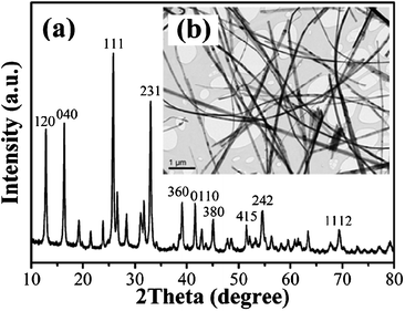 |
| | Fig. 1 (a) XRD pattern of the NH4Nb3O8 nanowires, (b) low magnification TEM image of the NH4Nb3O8 nanowires. | |
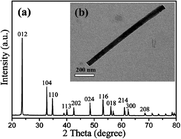 |
| | Fig. 2 (a) XRD pattern of the LiNbO3 nanowires, (b) low magnification TEM image of the LiNbO3 nanowires. | |
The detailed morphology and microstructure of the LiNbO3 nanowires are further characterized by TEM and HRTEM, as illustrated in Fig. 2b and Fig. 3a,b. Fig. 2b shows a typical TEM image of an individual LiNbO3 nanowire with a diameter of approximately 50 nanometers and a length of one micrometer. The high-resolution TEM image with the corresponding SAED pattern shown in Fig. 3a confirm that the obtained LiNbO3 nanowires are single-crystalline, and that the diffraction spots can be indexed to rhombic LiNbO3. As can be seen in Fig. 3b, the larger distance between two neighboring atomic planes is 3.75 Å, which can be indexed as (012) planes of a rhombic LiNbO3 crystal. The lattice spacing of 1.70 Å can correspond to the (116) plane of the rhombic LiNbO3. The nanowire axis grows along the c-axis direction of LiNbO3.
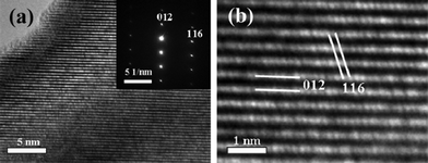 |
| | Fig. 3 (a) HRTEM image of the LiNbO3 nanowires, (b) The lattice fringe separations of 0.375 and 0.170 nm can be indexed as (012) and (116) lattice space respectively. | |
According to the experimental results and references,16–17 the probable chemical reaction through the whole process of the synthesis can be depicted as follows:
| | | (NH2)2CO + H2O → 2NH3 + CO2 | (1) |
| | | 6Nb + 2NH4OH + 14H2O → 2NH4Nb3O8 + 15H2 | (3) |
| | | 2NH4Nb3O8 → 3Nb2O5 + H2O + 2NH3 | (4) |
| | | Nb2O5 + Li2CO3 → 2LiNbO3 + CO2 | (5) |
First, the NH4Nb3O8 nanowires are formed through a hydrothermal reaction (see reactions 1–3). In the molten salt reaction, the NH4Nb3O8 nanowires will transform into Nb2O5 nanowires when they are heated at a high temperature. Finally, the Nb2O5 nanowires react with Li2CO3 powders in a KCl melt to yield LiNbO3 nanowires. The as-prepared LiNbO3 nanowires become much shorter than the NH4Nb3O8 nanowires. There might be two main causes for this phenomenon. First, the nanowires were mechanically broken, because the mixture needs to be ground together. Second, that result might be ascribed to a “breaking up” of wire-like NH4Nb3O8 and Nb2O5, which is similar to the phenomenon observed for wire-like H3ONb3O8 and KNb3O8.18 One long nanowire will probably break up into several short parts for the calcination at a high temperature and then react with Li2CO3 dissolved in a KCl molten salt by a topochemical reaction.
Raman spectra have provided an effective way to confirm the phase composition of alkaline niobate as a supplementary means, because each alkaline niobate has its own characteristic Raman spectrum due to their unique crystal structure. Fig. 4 shows Raman spectra of the as-prepared LiNbO3 nanowires. The main Raman peaks observed in Fig. 4 at 152, 238, 319, 369, and 433 cm−1 can be assigned to the E transverse optical (TO) phonon modes of LiNbO3. The peak at 617 cm−1 can be indexed to a mixing of A1 TO and E TO modes, the peak of quasi longitudinal optical (LO) phonon mode expected at 883 cm−1 shifted to a lower wavenumber of 873 cm−1. All peak positions in the spectrum can indicate further that pure phase LiNbO3 nanowires of high quality have been synthesized.17,19–20 The UV-vis diffuse reflectance spectrum of the LiNbO3 is shown in Fig. 5. From the UV-vis spectrum, the estimated band gap of the obtained LiNbO3 nanowires is approximately 4 eV. According to the reference,21–22 the indirect band gap value of LiNbO3 crystals obtained from the optical absorption experiment is in the range of 3.28 eV to 4.0 or 4.3 eV. Compared with the calculated band gap value of ideal LiNbO3 crystal, this value of 4 eV is bigger than the DFT calculation value but smaller than the GW calculation value. The absorption tail observed in Fig. 5 may be caused by defects of the LiNbO3 nanowires.
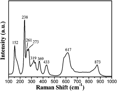 |
| | Fig. 4 Raman spectra of the LiNbO3 nanowires. | |
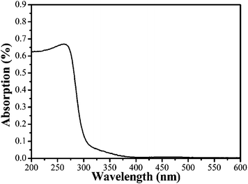 |
| | Fig. 5 UV-vis diffused spectra of the LiNbO3 nanowires. | |
To investigate piezoelectric response of an individual LiNbO3 nanowire, a PFM is employed, and a Pt–SiO2–Si substrate was used as a bottom electrode. Prior to the piezoelectric measurement, a small amount of LiNbO3 nanowire powder was dispersed in alcohol by ultrasonication, and a drop of the resulting suspension was deposited on the surface of the bottom electrode and dried. In order to improve adhesion of the nanowires to the Pt-coated surface, the substrate was annealed at 500 °C for 1 h. During the measurement, a slight alternating current (AC) voltage was applied between the bottom electrode and the conductive tip (force constant K = 0.2 N m−1, Cr–Pt coated). The displacement–voltage (D–V) “butterfly” curve was recorded by applying an AC voltage from −10 V to 10 V. The schematic diagram of the PFM experiment is exhibited in Fig. 6a. If the nanowires are too long or too high, they will be moved away during scanning, because their adhesion to the surface of the bottom electrode is too weak to resist the lateral force given by the atomic force microscopy tip. The LiNbO3 nanowire with a length of approximately 1.1 μm can be found in Fig. 6b, and a flat local region of the surface of the nanowire where the sample protrudes around 100 nm out of the surface is chosen for PFM measurement. As can be seen from the typical D–V “butterfly” curve shown in Fig. 6c, the LiNbO3 nanowire exhibits excellent piezoelectric response. Every point on the D–V “butterfly” loop contains information about piezoelectric deformation under a corresponding applied voltage. From the corresponding D–V “butterfly” curves, the d33-voltage (d33-V) loops (see Fig. 6d) can be determined viaeqn (6) of the piezoelectric effect:23–24
| |  | (6) |
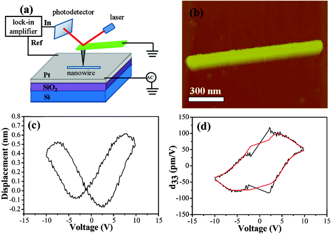 |
| | Fig. 6 (a) A schematic diagram of the PFM experiment on a typical LiNbO3 nanowire, (b) topographic image of a single LiNbO3 nanowire, (c) the typical D–V “butterfly” cure, and (d) the corresponding d33-V loop. | |
In eqn (6), D is the measured value of piezoelectric deformation, V is the applied voltage for each point on the D–V curve, DI is the piezoelectric deformation and VI is the applied voltage of the intersection. The values of d33 calculated from the D–V “butterfly” curves are usually deviated from the actual value a little for many reasons. For instance, the AFM tip could not always keep the upright position during the PFM measurements, and the measured D–V “butterfly” curve often includes the electrostrictive effect information of the tested material. However, the piezoelectric properties can be determined from the estimated d33 values to some extent. From our experimental results, the estimated max d33 value of the individual LiNbO3 nanowire can reach approximately 100 pm V−1. Therefore, LiNbO3 nanowire is a very important environmentally-friendly lead-free piezoelectric nanowire.
Conclusion
In summary, a hydrothermal route has been employed for the synthesis of NH4Nb3O8 nanowires, and the LiNbO3 nanowires can be prepared via the simple molten-salt reaction with Li2CO3 powders in melt KCl using NH4Nb3O8 nanowires as the starting material. The obtained rhombic LiNbO3 nanowires have pure phase and good crystallinity along the c-axis, and it has a band gap of 4 eV. Meanwhile, the PFM measurements on the LiNbO3 nanowire show strong piezoactivity. The maximum d33 value can reach approximately 100 pm V−1, which indicates the LiNbO3 nanowire is an excellent 1D environment-friendly lead-free piezoelectric material. It is a promising candidate in applications like integrated piezoelectric sensors, resonators, and NEMS related devices.
Acknowledgements
We thank Yanping Wei, Guoxin Chen, Meimei Liu, and Huanming Lu working at Ningbo Institute of Material Technology and Engineering belonging to the Chinese Academy of Sciences for the SPM and HRTEM measurements. We are also very grateful to Mingdeng Wei at Fuzhou University for his helpful suggestions.
References
- L. Louis, P. Gemeiner, I. Ponomareva, L. Bellaiche, G. Geneste, W. Ma, N. Setter and B. Dkhil, Nano Lett., 2010, 10, 1177 CrossRef CAS.
- J. Wang, C. Stampfer, C. Roman, W. H. Ma, N. Setter and C. Hierold, Appl. Phys. Lett., 2008, 93, 223101 CrossRef.
- T. Y. Ke, H. A. Chen, H. S. Sheu, J. W. Yeh, H. N. Lin, C. Y. Lee and H. T. Chiu, J. Phys. Chem. C, 2008, 112, 8827 CAS.
- H. Uršič, A. Benčan, M. Škarabot, M. Godec and M. Kosec, J. Appl. Phys., 2010, 107, 033705 CrossRef.
- C. Yan, L. Nikolova, A. Dadvand, C. Harnagea, A. Sarkissian, D. F. Perepichka, D. F. Xue and F. Rosei, Adv. Mater., 2010, 22, 1741 CrossRef CAS.
- F. Abdi, M. Aillerie, P. Bourson, M. D. Fontana and K. Polgar, J. Appl. Phys., 1998, 84, 2251 CrossRef CAS.
- Y. B. Wan, X. G. Guo, J. Che, X. Z. Yuan, J. H. Chu and J. Li, J. Cryst. Growth, 2002, 235, 248 CrossRef CAS.
- Y. Nakayama, P. J. Pauzauskie, A. Radenovic, R. M. Onorato, R. J. Saykally, J. Liphardt and P. eidong Yang, Nature, 2007, 447, 1098 CrossRef CAS.
- R. Grange, J. W. Choi, C. L. Hsieh, Y. Pu, A. Magrez, R. Smajda, L. Forro and D. Psaltis, Appl. Phys. Lett., 2009, 95, 143105 Search PubMed.
- Y. Saito, H. Takao, T. Tani, T. Nonoyama, K. Takatori, T. Homma, T. Nagaya and M. Nakamura, Nature, 2004, 432, 84 CrossRef CAS.
- L. Hao, J. Zhu, W. Luo, H. Zeng, L. Yanrong, W. Huang, X. Liao and Y. Zhang, Appl. Phys. Lett., 2009, 95, 232907 CrossRef.
- G. Suyal, E. Colla, R. Gysel, M. Cantoni and N. Setter, Nano Lett., 2004, 4, 1339 CrossRef CAS.
- F. Dutto, C. Raillon, K. Schenk and A. Radenovic, Nano Lett., 2011, 11, 2517 CrossRef CAS.
- K. Saito, K. Koga and A. Kudo, Dalton Trans., 2011, 40, 3909 RSC.
- J. Y. Huang, Z. Chen, Z. S. Zhang, C. Y. Zhu, H. P. He, Z. Z. Ye, G. Y. Qu and L. M. Tong, Appl. Phys. Lett., 2011, 98, 093102 CrossRef.
- M. D. Wei, Z. M. Qi, M. Ichihara and H. S. Zhou, Acta Mater., 2008, 56, 2488 CrossRef CAS.
- A. C. Santulli, H. J. Zhou, S. Berweger, M. B. Raschke, E. Sutter and S. S. Wong, CrystEngComm, 2010, 12, 2675 RSC.
- L. H. Li, J. X. Deng, J. Chen, X. Y. Sun, R. B. Yu, G. R. Liu and X. R. Xing, Chem. Mater., 2009, 21, 1207 CrossRef CAS.
- E. R. Camargo and M. Kakihana, Chem.
Mater., 2001, 13, 1905 CrossRef CAS.
- P. Heitjans, M. Masoud, A. Feldhoff and M. Wilkening, Faraday Discuss., 2007, 134, 67 RSC.
- C. Thierfelder, S. Sanna, A. Schindlmayr and W. G. Schmidt, Phys. Status Solidi C, 2010, 2, 362 CrossRef.
- J. Zhu, S. Zhao, D. Xiao, X. Wang and G. Xu, J. Phys.: Condens. Matter, 1992, 4, 2977 CrossRef CAS.
- Y. C. Yang, C. Song, X. H. Wang, F. Zeng and F. Pan, Appl. Phys. Lett., 2008, 92, 012907 CrossRef.
- Y. Q. Chen, X. J. Zheng and X. Feng, Nanotechnology, 2010, 21, 055708 CrossRef CAS.
|
| This journal is © The Royal Society of Chemistry 2012 |
Click here to see how this site uses Cookies. View our privacy policy here.