Silicon@porous nitrogen-doped carbon spheres through a bottom-up approach are highly robust lithium-ion battery anodes†
Hyung Mo
Jeong
a,
Su Yeon
Lee
b,
Weon Ho
Shin
b,
Jun Ho
Kwon
a,
Abdul
Shakoor
a,
Tae Hoon
Hwang
b,
Se Yun
Kim
a,
Byung-Seon
Kong
c,
Jin-Seok
Seo
c,
Yong Min
Lee
d,
Jeung Ku
Kang
*ab and
Jang Wook
Choi
*b
aDepartment of Materials Science and Engineering, Korea Advanced Institute of Science and Technology, Daejeon, Republic of Korea. E-mail: Jeungku@kaist.ac.kr; Fax: +82-42-350-3338; Tel: +82-42-350-3338
bKAIST Institute NanoCentury and Graduate School of EEWS(WCU), Korea Advanced Institute of Science and Technology, Daejeon, Republic of Korea. E-mail: jangwookchoi@kaist.ac.kr; Fax: +82-42-350-1719; Tel: +82-42-350-1719
cKCC Central Research Institute, Yongin, Republic of Korea
dDepartment of Applied Chemistry, Hanbat National University, Daejeon, Republic of Korea
First published on 7th March 2012
Abstract
Due to its excellent capacity, around 4000 mA h g−1, silicon has been recognized as one of the most promising lithium-ion battery anodes, especially for future large-scale applications including electrical vehicles and utility power grids. Nevertheless, Si suffers from a short cycle life as well as limitations for scalable electrode fabrication. Herein, we report a novel design for highly robust and scalable Si anodes: Si nanoparticles embedded in porous nitrogen-doped carbon spheres (NCSs). The porous nature of NCSs buffers the volume changes of Si nanoparticles and thus resolves critical issues of Si anode operations, such as pulverization, vulnerable contacts between Si and carbon conductors, and an unstable solid-electrolyte interphase. The unique electrode structure exhibits outstanding performance with a gravimetric capacity as high as 1579 mA h g−1 at a C/10 rate based on the mass of both Si and C, a cycle life of 300 cycles with 94% capacity retention, as well as a discharge rate capability of 6 min while retaining a capacity of 702 mA h g−1. Significantly, the coulombic efficiencies of this structure reach 99.99%. The assembled structure suggests a design principle for high capacity alloying electrodes that suffer from volume changes during battery operations.
1. Introduction
Among diverse secondary batteries, lithium-ion batteries (LIBs) have been the most promising energy storage system for next generation portable electronics, electrified vehicles (EVs), and utility grid applications1,2 because of their outstanding performance in energy density and power performance. In particular, their high energy densities are very attractive for EV applications because energy density is directly related to driving distance upon each charge. Along these lines, silicon (Si) has attracted remarkable attention on account of its unparalleled theoretical capacity, near 4000 mA h g−1, which is about 10 times higher than those of the current commercial graphite anodes.3,4 Despite its exceptional theoretical capacity, however, the use of Si has been quite limited because cycle lives of Si electrodes are rather inferior compared to those of graphite electrodes. The limited cycle life is caused mostly by the volume expansion of Si during lithiation. Upon full lithiation, Si undergoes a volume expansion of up to 300%.5,6The volume expansion of Si typically leads to three failure mechanisms: (1) Si can fracture because of the stress generated during the volume expansion. This fracture issue is, however, resolved by the small dimensions of the active materials that enable adequate stress relaxation. Utilizing the advantages of small dimensions, various nanostructured Si electrodes, including nanowires,7–13 nanoparticles (NPs),14,15 and nanotubes,16,17 have been developed for improved cycling performance. (2) Si active materials can lose their contacts with carbon (C) conductors during repeated volume expansion and shrinkage. The lost contacts produce dead portions of Si active materials, and thus cause capacity decay. Similarly, the repeated volume change of Si causes Si active materials to unbind from the electrode films, and therefore Si active materials can be peeled off from current collectors. (3) During cycling, the solid-electrolyte-interphase (SEI) layers on the Si surfaces are vulnerable, due to the stress originating from repeated volume changes of Si, and therefore become mechanically unstable. As a result, cracks are frequently formed along SEI layers. In the subsequent cycles, SEI layers grow continuously through these cracks, and eventually the growth of SEI layers reaches a point where Li ions can no longer diffuse through the SEI layers. Also, the successive SEI growth is usually accompanied by electrolyte consumption. Thus, the electrolyte can be exhausted.
Based on these concerns, a question naturally arises: what would be the ideal Si electrode structure that addresses the aforementioned issues, and, at the same time, is scalable? To this end, in this study, we chose Si NPs as Si active materials, from various Si nanostructures, because Si NPs are most feasible for mass production and have indeed been commercially available for a while. Also, in order to overcome the problem of contact with carbon conductors as well as the unstable SEI problem, a bottom-up approach was employed to build a robust Si–C composite structure where Si NPs are embedded into nitrogen-doped mesoporous carbon spheres, namely nitrogen-doped carbon spheres (NCSs). More specifically, the porous nature of NCSs can accommodate the volume expansion of Si NPs. As a result, the overall spherical structures, and thus the electrical contacts between Si NPs and carbon conductors, are well preserved throughout cycling. The robust spherical structures also allow SEI layers to remain stable both on the outer surfaces of and inside NCSs during repeated volume changes of Si. Based on this unique electrode structure, Si NPs embedded in NCSs exhibit outstanding performance with a gravimetric capacity as high as 1579 mA h g−1 at a C/10 rate based on the mass of both Si and C, a cycle life of 300 cycles with 94% capacity retention, coulombic efficiencies of around 99.99% as well as a discharge rate capability of 6 min, while retaining a capacity of 702 mA h g−1. Moreover, the entire processes for the electrode fabrication should be adaptable to large-scale manufacturing processes because all the cell components are commercially available and the whole procedure consist of two simple steps free from any sensitive conditions. Previously, some Si–C composite electrodes were reported.15,18–27 In most of these Si–C structures, however, more severe capacity decays were observed, or cycling data only below 50 cycles were presented.15,20–26 Perhaps these limited cycle lives originate from their composite structures being unable to accommodate the volume expansion of Si. Also, in some reports, the mass portions of Si were too low, smaller than 30 wt.%.19–21
2. Experimental section
2.1 Synthesis of Si@NCS
We first added 5.0225 g melamine to 8.846 mL formaldehyde aqueous solution (120 mM) in 40 mL deionized (DI) water. After heating at 100 °C for 8 min, MF sol was obtained. 500 mg Si nanoparticles (KCC Corp., Korea) were dispersed in 50 mL DI water, and this Si solution was added to the MF sol. 60 mL Pluronic F127 (6 g) aqueous solution was added to the solution. The solution was then stirred in the presence of 400 μL 1 M hydrochloric acid (HCl) at 100 °C for 24 h. The condensation reaction took place and Si@MFS was produced. Si@MFS was washed several times by centrifugation in the co-solvents of water and ethanol (1![[thin space (1/6-em)]](https://www.rsc.org/images/entities/char_2009.gif) :1, v/v). Finally, Si@NCS was obtained after a sequential heat treatment (400 °C for 2 h, 600 °C for 2 h, 800 °C for 2 h). The heating rate was 1 °C min−1.
:1, v/v). Finally, Si@NCS was obtained after a sequential heat treatment (400 °C for 2 h, 600 °C for 2 h, 800 °C for 2 h). The heating rate was 1 °C min−1.
2.2 Characterization
To observe the morphologies of various samples, we used SEM (HITACHI, S-4800) and Cs-corrected scanning TEM (JEOL, JEM-ARM200F). An energy dispersive spectrometer (EDS) attached on the TEM apparatus was used to obtain local elemental information. XRD (RIGAKU, D/MAX-IIIC), XPS (Thermo VG Scientific, Sigma Probe), and BET (Quantachrome, Quadrasorb SI) measurements were performed to analyze the crystal structures, atomic bonding configurations, and porosities of various samples, respectively. The Si weight portion was calculated based on thermogravimetric analysis (TGA) (Netzsch, TG 209 F3) measurements. In order to image the morphologies after cycling, the coin cells were opened and the electrodes were thoroughly washed with acetonitrile inside a glove box. Then, the samples were transferred into petri dishes and the dishes were completely sealed to prevent exposure to air. The samples were exposed to air for < 30 s during the transfer to vacuum chambers for SEM or TEM.2.3 Electrochemical measurement
For the electrode fabrication, slurries were first prepared by dissolving 80 wt.% active materials, 5 wt.% polyvinylidene fluoride (PVDF), 5 wt.% polyacrylic acid (PAA), and 10 wt.% Super-P in N-methyl-2-pyrrolidone (NMP). After casting the slurries onto Cu foil, the electrodes were dried at 80 °C under vacuum overnight. The mass loadings of active materials were ∼1 mg cm−2. To test the electrochemical properties, 2032 type coin cells were prepared by assembling the prepared working electrodes, Celgard 2400 separators, and Li metal foil (Honjo Chemical Co.). 1 M lithium hexafluorophosphate (LiPF6), dissolved in co-solvents ethylene carbonate (EC) and diethyl carbonate (DEC) (EC–DEC = 1:1, v/v) was used as the electrolyte. All of the cell assembly procedures were done in an argon-filled glove box. The electrodes were cycled in the potential range 0.02 V∼1.5 V (vs Li/Li+) for Si-based electrodes and 0.005 V∼3 V for NCS electrodes at room temperature using a battery cycler (Wonatech, WBCS-3000). Cyclic voltammetry characterization was performed at a rate of 0.025 mV s−1 in the potential window of 0 to 1.5 V using a potentiostat (Wonatech, WEIS 500). Electrochemical impedance spectra (EIS) measurements were carried out using a multichannel impedance cycler (BIOLOGIC, VSP). The frequency range was from 10 mHz to 1000 kHz and the amplitude was 5 mV. The data in Fig. 4e were obtained after discharge (delithiation) of each cycle.
3. Results and discussion
As summarized in Fig. 1, the preparation of Si NPs embedded in NCSs consists simply of two steps—a condensation step followed by an annealing step. For the condensation, a mixture of melanin-formaldehyde (MF) resin, surfactant (Pluronic F127), and Si NPs (KCC, Korea) was stirred in deionized (DI) water at 100 °C. It is noteworthy that amine groups in MF can form strong hydrogen bonds with hydroxyl groups on the Si NP surfaces.28,29 The hydrogen bonds endow Si NPs with close interactions with the MF resin. Thus, once the condensation is completed, all the Si NPs can be embedded in MF spheres (MFSs). Next, the MFSs were annealed at several different temperatures up to 800 °C to carbonize MF to nitrogen (N-doped carbon). After this carbonization step, the final structure of Si NPs embedded in N-doped carbon spheres is produced. See the Experimental section for a more detailed description. For simplicity, Si NPs embedded in NCSs, NCSs alone, and Si NPs alone are hereafter denoted as Si@NCS, NCS, and SiNP, respectively.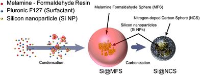 | ||
| Fig. 1 Experimental synthetic procedures for nitrogen-doped carbon spheres containing Si NPs (Si@NCS). A mixture of MF resins, Pluronic F127, and Si NPs was first condensed and then carbonized. | ||
From scanning electron microscopy (SEM) images of NCS (Fig. 2a and b) and Si@NCS (Fig. 2c and d), it can be noted that the original spherical shapes of NCS are preserved even after the incorporation of Si NPs into NCSs. But, by containing Si NPs, the sphere sizes decrease from 1.5 μm to 0.7 μm, presumably because smaller spheres can more efficiently relax the stress that is created by the inclusion of Si NPs within NCSs. Also, the surfaces of Si@NCS are rougher than those of NCS, once again due to the inclusion of Si NPs. While the samples (Fig. 2e) scraped off from the electrode films show aggregated Si@NCSs, a transmission electron microscopy (TEM) image (Fig. 2f) of an individual Si@NCS verifies that the Si NPs are completely wrapped by the NCSs. Consequently, it is expected that the Si NPs will remain electrically in contact with carbon conducting components during cycling. Elemental analyses were also conducted (Fig. 2g) for the same Si@NCS using scanning transmission electron microscopy (STEM), and it is confirmed that the dark spots of the TEM image are indeed Si NPs. The Si NPs used in this study are approximately 30 nm in diameter (Fig. S1†).
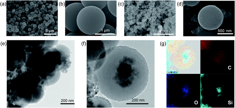 | ||
| Fig. 2 Characterization of Si@NCS. SEM images of NCS at (a) low and (b) high magnification. SEM images of Si@NCS at (c) low and (d) high magnification. (e) A TEM image of Si@NCS cast with carbon conductors and binders for electrodes. (f) A TEM image of Si@NCS at single-sphere resolution. (g) STEM images for the same Si@NCS as in (f) were obtained for elemental analyses. Elemental mappings for carbon, oxygen, Si, and their combination are presented. | ||
Si@NCSs were characterized further, focusing on their crystal structures, atomic configurations, and porosities. As displayed in Fig. 3a, an X-ray diffraction (XRD) pattern of NCS exhibits broad peaks at 25 and 43°, which correspond to the (002) and (101) planes of the NCS, respectively.30,31 Si@NCS exhibits not only the vague peaks originating from NCS, but also the peaks corresponding to the (111), (220), (311), (400), and (331) planes of Si, therefore confirming the inclusion of Si NPs in NCSs.
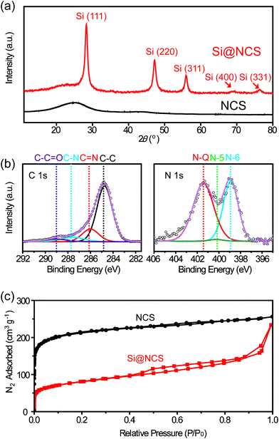 | ||
| Fig. 3 (a) XRD patterns of Si@NCS and NCS. (b) XPS data measured in the regions of C 1s and N 1s for Si@NCS. (c) BET isotherms for Si@NCS and NCS. | ||
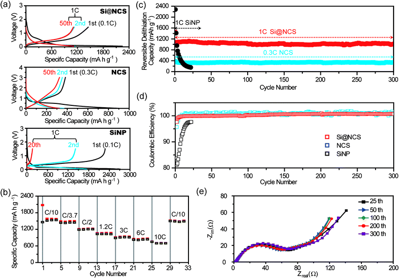 | ||
| Fig. 4 (a) Potential profiles for Si@NCS, NCS, and SiNP at different cycle numbers. (b) A rate capability test for Si@NCS measured at 0.1C–10C. (c) The cycling performances and (d) coulombic efficiencies of Si@NCS, NCS, and SiNP. (e) Impedance spectra of Si@NCS after delithiation at the 25th, 50th, 100th, and 200th cycles. All of the data of Si@NCS shown in this figure are based on the masses of both Si and C. Also, in Si@NCS, Si accounts for 50 wt.%. | ||
X-Ray photoelectron spectroscopy (XPS) measurements (Fig. 3b) elucidate atomic configurations of Si@NCS, particularly carbon and nitrogen. The C 1s data show the peaks corresponding to C–C, C![[double bond, length as m-dash]](https://www.rsc.org/images/entities/char_e001.gif) N, and C–N bonds, which are characteristic of atomic configurations of NCSs.32–35 The C 1s data also exhibit the C–CO peak, and thus indicate the chemical interaction between silicon oxide on the Si NP surfaces and carbon in the NCSs, which will play an important role in electronic diffusion during battery operations. On the other hand, the N 1s data provide information on the bonding configurations between carbon and nitrogen. After the carbonization of the MF resins, three C–N configurations are typically produced: N-Q (graphite-like, 401.5 eV), N-5 (pyrrole-like, 400.1 eV), and N-6 (pyridine-like, 398.9 eV). The existence of these N-configurations is consistent with previous studies that used MF resins as starting materials.33,36,37 After carbonization at 800 °C, unlike the N-6 and N-Q peaks, the N-5 peak is hardly observed in the N 1s spectrum of Si@NCS. These results indicate that during the annealing process, N-5 turns into N-6 and N-Q, both of which are known to be more stable at high temperatures.38 The increased proportion of N-Q is expected to increase the electronic conductivity of NCS.39 Also, the XPS data imply that the nitrogen contents for NCS and Si@NCS are 8.03% and 7.78%, respectively (Table S1†).
N, and C–N bonds, which are characteristic of atomic configurations of NCSs.32–35 The C 1s data also exhibit the C–CO peak, and thus indicate the chemical interaction between silicon oxide on the Si NP surfaces and carbon in the NCSs, which will play an important role in electronic diffusion during battery operations. On the other hand, the N 1s data provide information on the bonding configurations between carbon and nitrogen. After the carbonization of the MF resins, three C–N configurations are typically produced: N-Q (graphite-like, 401.5 eV), N-5 (pyrrole-like, 400.1 eV), and N-6 (pyridine-like, 398.9 eV). The existence of these N-configurations is consistent with previous studies that used MF resins as starting materials.33,36,37 After carbonization at 800 °C, unlike the N-6 and N-Q peaks, the N-5 peak is hardly observed in the N 1s spectrum of Si@NCS. These results indicate that during the annealing process, N-5 turns into N-6 and N-Q, both of which are known to be more stable at high temperatures.38 The increased proportion of N-Q is expected to increase the electronic conductivity of NCS.39 Also, the XPS data imply that the nitrogen contents for NCS and Si@NCS are 8.03% and 7.78%, respectively (Table S1†).
The porosities of NCSs and Si@NCS were characterized by BET (Brunauer–Emmett–Teller) measurements (Fig. 3c). Clearly, the pore volumes of Si@NCS are much smaller than those of NCS, indicating that the insertion of Si NPs into NCSs decreases the porosity significantly. For the same reason, after the insertion of Si NPs, the BET surface area decreases from 800 to 244 m2 g−1. In addition, both samples show distinct isotherm shapes, reflecting different natures of porosity. Si@NCS exhibits a clear hysteresis between adsorption and desorption and thus indicates that Si@NCS contains mesopores (2–50 nm). By contrast, NCS exhibits no hysteresis but a higher pore volume, which is reflective of a porosity character composed mainly of micropores (< 2 nm). The presence of mesopores in Si@NCS is associated with the inter-space between Si NPs and NCSs formed based on the volume shrinkage of MFSs during the carbonization process. Pore size distributions also support these pore dimensions (Fig. S2†).
In order to investigate the structural effect of Si@NCS on the battery performance, Si@NCS was electrochemically tested by preparing coin-type half-cells in which Li foil was used as both the counter and reference electrodes. 1 M LiPF6, dissolved in the co-solvents of ethylene carbonate (EC)–diethylene carbonate (DEC) (1:1 = v:v), was used as an electrolyte. See the Experimental section for detailed procedures of the electrode fabrication and electrochemical measurements. Potential profiles for Si@NCS, NCS, and SiNP are presented in Fig. 4a. The charging (lithiation) and discharging (delithiation) of Si@NCS take place at around 0.2 and 0.5 V, respectively, while a discharge capacity of 1579 mA h g−1 is obtained at a 0.1C rate (1C: charge and discharge take 1 h each). These potentials are characteristic of charge–discharge operations of Si.8,14,40 In particular, Si@NCS exhibits a conspicuous plateau at ∼0.1 V during lithiation in the first cycle, which corresponds to the phase transition of nanostructured Si from crystalline to amorphous.8,22 Once this phase transition takes place, Si remains amorphous thereafter, and thus plateaus become steeper in the delithiation of the first cycle and subsequent cycles. The coulombic efficiency (CE) of Si@NCS in the first cycle is 71%. The irreversible capacity in the first cycle can be ascribed to SEI formation on the micropore surfaces of NCSs with large surface areas.15,41 However, the efficiency can be improved significantly by increasing the Si:C ratio.
By contrast, NCS shows less defined plateaus with steeper slopes, which is consistent with the data for soft carbon based anodes.42 From these potential profiles, it is apparent that the specific capacities of NCS (340 mA h g−1) are substantially lower than those of Si@NCS, once again due to the absence of Si. The CE of NCS in the first cycle is only 42%, which again reflects irreversible SEI formation on the very large surfaces of NCS micropores. On the other hand, SiNP displays its highest discharge capacity of 2277.8 mAh g−1 in the first cycle with a CE of 80% due to the higher portion of Si. However, SiNP suffers from pretty rapid capacity decay over cycling and, in fact, this control sample loses its entire capacity after only 20 cycles. Thus, the significantly enhanced cycle life of Si@NCS implies the importance of the electrode design in Si@NCS for repeated cycling. In addition, cyclic voltammetry (CV) characterization (Fig. S3†) was performed for Si@NCS. Consistently with the galvanostatic measurements in Fig. 4a, the CV scans exhibit the characteristic Si anode behaviors: (i) a larger current density at 0.06 V during lithiation in the first cycle, (ii) broader lithiation/delithiation peaks after the first lithiation, and (iii) the retention of the peaks during successive cycles. All the gravimetric capacity data related to Si@NCS are based on the mass of both Si and C. Also, all the electrochemical data of Si@NCS are from the samples in which Si accounts for 50 wt.% as indicated by thermogravimetric analyses (Fig. S4†).
Moreover, Si@NCS exhibits excellent rate capabilities (Fig. 4b). Even at a 10C rate where charge–discharge takes only 6 min, a specific capacity of 702 mA h g−1 is retained. Similarly, even when the current density is increased 50-fold from 150 to 7500 mA g−1 (from 0.1C to 10C), 45% of the original capacity (1571 and 702 mA h g−1) is still retained. By contrast, the rate capability of Si NP was hardly measurable due to its severe capacity decay with cycling. The outstanding power performance of Si@NCS can be attributed to its electrode structure where Si NPs are in direct contact with NCSs, which facilitates good electronic transport. Also, it is likely that the N-Q formation in NCSs contributes to the excellent rate capability, as N-Q has been known to increase the electronic conductivities by generating excessive electrons.38,39,43 In addition, the intrinsically small dimensions (∼30 nm) of Si NPs must also play a role by decreasing electronic and ionic diffusion lengths over Si active materials.
Most importantly, Si@NCS shows decent capacity retention for a large number of cycles (Fig. 4c). Once again, the cycling performance is the most critical and challenging aspect of Si anode operations. When cycled at a 1C rate, Si@NCS retains 94% of its initial capacity after 300 cycles. This retention is substantially superior to that of SiNP in our control experiments as well as those of most nanostructured Si electrodes,7,20,22,25,44–48 and thus verifies that the electrode structure of Si@NCS is critical for very robust cycling. Obviously, the decent cycling performance implies that Si@NCS maintains stable SEI layers.
Along these lines, we speculate that the porous NCSs play a critical role in promoting and preserving stable SEI layers: although Si NPs undergo significant volume changes during cycling, as evidenced by the high gravimetric capacities, the entire surfaces of Si NPs are mostly in direct contact with carbon. Therefore, the mechanically unstable SEI which was fatal to the cycle lives of most Si electrodes with no such carbon contacts can be avoided. Rather, it is more likely that the porous nature of NCS buffers the volume change of Si and therefore prevents SEI layers from growing in an uncontrolled manner beyond NCSs. In other words, once SEI layers are saturated within NCSs, the SEI layers remain stable throughout cycling despite the continuous volume changes of Si. This SEI layer stabilization is reflected clearly in CE data (Fig. 4d). The CEs of Si@NCS increase continuously from the early period of cycling and reach 99.99% at around 50 cycles, which can be interpreted as the SEI layers becoming stabilized in the NCSs during the 50 cycles. These CEs are preserved persistently thereafter. These CE values are quite remarkable for Si electrodes and are even comparable to those of graphite electrodes.49–51 Also, these values are clearly superior to those of most reported Si anodes.22,24,26,44,46 In addition, the stable SEI formation throughout cycling was quantitatively proved by electrochemical impedance spectroscopy (EIS) measurements (Fig. 4e). The EIS data show similar diameters of semi-circles for a large number of cycles, which represent consistent interfacial resistance and thus support the stable SEI.
In order to confirm the structural robustness, the electrodes were imaged after 400 cycles using SEM and TEM (Fig. 5). As shown in Fig. 5a and b, the spherical shapes of Si@NCS are clearly preserved. This observation suggests that Si NPs remain embedded within NCSs and thus maintain the electrical contacts with NCSs over cycling. The presence of Si NPs in NCSs was further verified (Fig. 5c) by STEM characterization. As indicated by the line profile (yellow line in Fig. 5c), the higher Si intensities were detected at several middle points in the NCS. The Si signal, however, clearly disappears as the line goes outside the NCS. Overall, the electrode structure of Si@NCS is well maintained for a large number of cycles, supporting the decent cycling performance.
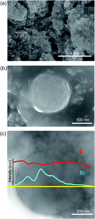 | ||
| Fig. 5 SEM images of the electrode structure of Si@NCS after 400 cycles at (a) low and (b) high magnification. (c) A TEM image showing Si@NCS at a single NCS scale, alongside elemental mapping measured along the yellow line. | ||
4. Conclusions
This investigation suggests a simple design principle for highly robust Si anodes: the integration of porous conductive materials with nanostructured Si for buffering the significant volume changes of Si and thus resolving the critical interfacial issues. Moreover, the entire procedure is scalable because each experimental step is simple and starting materials are all commercially available. This approach should also be immediately applicable to other LIB electrode materials that undergo large volume changes during cycling.Acknowledgements
J. W. C. and J. K. K. acknowledge the National Research Foundation of Korea Grant funded by the Korean Government (MEST) for the financial support through the Secondary Battery Program (NRF-C1AAA001-2010-0029031) and the World Class University Program (R-31-2008-000-10055-0) for the financial support.References
- M. Armand and J. M. Tarascon, Nature, 2008, 451, 652–657 CrossRef CAS.
- J. B. Goodenough and Y. Kim, Chem. Mater., 2010, 22, 587–603 CrossRef CAS.
- B. A. Boukamp, G. C. Lesh and R. A. Huggins, J. Electrochem. Soc., 1981, 128, 725–729 CrossRef CAS.
- U. Kasavajjula, C. Wang and A. J. Appleby, J. Power Sources, 2007, 163, 1003–1039 CrossRef CAS.
- H. Robert A, J. Power Sources, 1999, 81–82, 13–19 Search PubMed.
- L. Y. Beaulieu, K. W. Eberman, R. L. Turner, L. J. Krause and J. R. Dahn, Electrochem. Solid-State Lett., 2001, 4, A137–A140 CrossRef CAS.
- C. K. Chan, R. N. Patel, M. J. O'Connell, B. A. Korgel and Y. Cui, ACS Nano, 2010, 4, 1443–1450 CrossRef CAS.
- C. K. Chan, H. L. Peng, G. Liu, K. McIlwrath, X. F. Zhang, R. A. Huggins and Y. Cui, Nat. Nanotechnol., 2008, 3, 31–35 CrossRef CAS.
- H. X. Chen, Y. Xiao, L. Wang and Y. Yang, J. Power Sources, 2011, 196, 6657–6662 CrossRef CAS.
- J. W. Choi, J. McDonough, S. Jeong, J. S. Yoo, C. K. Chan and Y. Cui, Nano Lett., 2010, 10, 1409–1413 CrossRef CAS.
- K. Kang, H. S. Lee, D. W. Han, G. S. Kim, D. Lee, G. Lee, Y. M. Kang and M. H. Jo, Appl. Phys. Lett., 2010, 96, 053110 CrossRef.
- N. A. Liu, L. B. Hu, M. T. McDowell, A. Jackson and Y. Cui, ACS Nano, 2011, 5, 6487–6493 CrossRef CAS.
- K. Kang, K. Song, H. Heo, S. Yoo, G.-S. Kim, G. Lee, Y.-M. Kang and M.-H. Jo, Chem. Sci., 2011, 2, 1090–1093 RSC.
- H. Kim, M. Seo, M. H. Park and J. Cho, Angew. Chem., Int. Ed., 2010, 49, 2146–2149 CrossRef CAS.
- S. H. Ng, J. Z. Wang, D. Wexler, K. Konstantinov, Z. P. Guo and H. K. Liu, Angew. Chem., Int. Ed., 2006, 45, 6896–6899 CrossRef CAS.
- M. H. Park, M. G. Kim, J. Joo, K. Kim, J. Kim, S. Ahn, Y. Cui and J. Cho, Nano Lett., 2009, 9, 3844–3847 CrossRef CAS.
- T. Song, J. L. Xia, J. H. Lee, D. H. Lee, M. S. Kwon, J. M. Choi, J. Wu, S. K. Doo, H. Chang, W. Il Park, D. S. Zang, H. Kim, Y. G. Huang, K. C. Hwang, J. A. Rogers and U. Paik, Nano Lett., 2010, 10, 1710–1716 CrossRef CAS.
- G. X. Wang, J. H. Ahn, J. Yao, S. Bewlay and H. K. Liu, Electrochem. Commun., 2004, 6, 689–692 CrossRef CAS.
- Y.-S. Hu, R. Demir-Cakan, M.-M. Titirici, J.-O. Müller, R. Schlögl, M. Antonietti and J. Maier, Angew. Chem., Int. Ed., 2008, 47, 1645–1649 CrossRef CAS.
- H.-Y. Lee and S.-M. Lee, Electrochem. Commun., 2004, 6, 465–469 CrossRef CAS.
- M. K. Datta and P. N. Kumta, J. Power Sources, 2007, 165, 368–378 CrossRef CAS.
- H. Kim and J. Cho, Nano Lett., 2008, 8, 3688–3691 CrossRef CAS.
- I.-S. Kim, G. E. Blomgren and P. N. Kumta, J. Power Sources, 2004, 130, 275–280 CrossRef CAS.
- P. Gu, R. Cai, Y. Zhou and Z. Shao, Electrochim. Acta, 2010, 55, 3876–3883 CrossRef CAS.
- Y. X. Yin, S. Xin, L. J. Wan, C. J. Li and Y. G. Guo, J. Phys. Chem. C, 2011, 115, 14148–14154 CAS.
- N. Dimov, S. Kugino and M. Yoshio, Electrochim. Acta, 2003, 48, 1579–1587 CrossRef CAS.
- T. H. Hwang, Y. M. Lee, B.-S. Kong, J.-S. Seo and J. W. Choi, Nano Lett., 2012, 12, 802–807 CrossRef CAS.
- L. D. White and C. P. Tripp, J. Colloid Interface Sci., 2000, 232, 400–407 CrossRef CAS.
- G. R. Bogart and D. E. Leyden, J. Colloid Interface Sci., 1994, 167, 27–34 CrossRef CAS.
- Y. Xia, Z. Yang and R. Mokaya, J. Phys. Chem. B, 2004, 108, 19293–19298 CrossRef CAS.
- Y. Xia and R. Mokaya, Chem. Mater., 2005, 17, 1553–1560 CrossRef CAS.
- C. Ronning, H. Feldermann, R. Merk, H. Hofsass, P. Reinke and J. U. Thiele, Phys. Rev. B, 1998, 58, 2207–2215 CrossRef CAS.
- C. Li, X. Yang, B. Yang, Y. Yan and Y. Qian, Mater. Chem. Phys., 2007, 103, 427–432 CrossRef CAS.
- A. P. Dementjev, A. de Graaf, M. C. M. van de Sanden, K. I. Maslakov, A. V. Naumkin and A. A. Serov, Diamond Relat. Mater., 2000, 9, 1904–1907 CrossRef CAS.
- K. Yamamoto, Y. Koga and S. Fujiwara, Diamond Relat. Mater., 2001, 10, 1921–1926 CrossRef CAS.
- D. Hulicova, J. Yamashita, Y. Soneda, H. Hatori and M. Kodama, Chem. Mater., 2005, 17, 1241–1247 CrossRef CAS.
- B. Friedel and S. Greulich-Weber, Small, 2006, 2, 859–863 CrossRef CAS.
- F. Su, C. K. Poh, J. S. Chen, G. Xu, D. Wang, Q. Li, J. Lin and X. W. Lou, Energy Environ. Sci., 2011, 4, 717–724 CAS.
- H. M. Jeong, J. W. Lee, W. H. Shin, Y. J. Choi, H. J. Shin, J. K. Kang and J. W. Choi, Nano Lett., 2011, 11, 2472–2477 CrossRef CAS.
- H. Ma, F. Cheng, J. Y. Chen, J. Z. Zhao, C. S. Li, Z. L. Tao and J. Liang, Adv. Mater., 2007, 19, 4067–4070 CrossRef CAS.
- Y.-P. Wu, C.-R. Wan, C.-Y. Jiang, S.-B. Fang and Y.-Y. Jiang, Carbon, 1999, 37, 1901–1908 CrossRef CAS.
- J. R. Dahn, A. K. Sleigh, H. Shi, J. N. Reimers, Q. Zhong and B. M. Way, Electrochim. Acta, 1993, 38, 1179–1191 CrossRef CAS.
- M. Seredych, D. Hulicova-Jurcakova, G. Q. Lu and T. J. Bandosz, Carbon, 2008, 46, 1475–1488 CrossRef CAS.
- W. Wang and P. N. Kumta, ACS Nano, 2010, 4, 2233–2241 CrossRef CAS.
- I. S. Kim and P. N. Kumta, J. Power Sources, 2004, 136, 145–149 CrossRef CAS.
- L.-F. Cui, Y. Yang, C.-M. Hsu and Y. Cui, Nano Lett., 2009, 9, 3370–3374 CrossRef CAS.
- C. K. Chan, R. Ruffo, S. S. Hong, R. A. Huggins and Y. Cui, J. Power Sources, 2009, 189, 34–39 CrossRef CAS.
- X. Chen, K. Gerasopoulos, J. Guo, A. Brown, C. Wang, R. Ghodssi and J. N. Culver, ACS Nano, 2010, 4, 5366–5372 CrossRef CAS.
- M. Winter, J. O. Besenhard, M. E. Spahr and P. Novák, Adv. Mater., 1998, 10, 725–763 CrossRef CAS.
- S. Flandrois and B. Simon, Carbon, 1999, 37, 165–180 CrossRef CAS.
- M. Endo, Y. A. Kim, T. Hayashi, K. Nishimura, T. Matusita, K. Miyashita and M. S. Dresselhaus, Carbon, 2001, 39, 1287–1297 CrossRef CAS.
Footnote |
| † Electronic Supplementary Information (ESI) available: SEM image of Si NPs, elemental contents by XPS measurements and pore size distribution of Si@NCS and NCS, cyclic voltammetric measurements, and thermal behavior of Si@NCS. See DOI: 10.1039/c2ra20170d/ |
| This journal is © The Royal Society of Chemistry 2012 |