Synthesis of hybrid polymethacrylate–noble metal (M = Au, Pd) nanoparticles for the growth of metal-oxide semiconductor nanowires
M.
Zervos
*a,
M.
Demetriou
b,
T.
Krasia-Christoforou
b,
A.
Othonos
c and
R. P.
Turcu
d
aNanostructured Materials & Devices Laboratory, School of Engineering, University of Cyprus, P.O. Box 20537, Nicosia, 1678, Cyprus. E-mail: zervos@ucy.ac.cy
bPolymers Laboratory, Materials Science Research Group, Department of Mechanical and Manufacturing Engineering, School of Engineering, University of Cyprus, P.O. Box 20537, Nicosia, 1678, Cyprus
cResearch Center of Ultrafast Science, Department of Physics, School of Physical Sciences, University of Cyprus, P.O. Box 20537, Nicosia, 1678, Cyprus
dNational Institute for Isotopic and Molecular Technologies, Cluj-Napoca 400293, Romania
First published on 10th April 2012
Abstract
Metal-oxide semiconductor nanowires (NWs) such as ZnO, β-Ga2O3 and SnO2 with diameters of tens of nanometres and lengths of many micrometres have been grown using micellar nanohybrids consisting of methacrylate-based diblock copolymers and noble metal nanoparticles (MNPs). Micellar Au and Pd MNPs with diameters as small as 2.3 ± 0.3 nm were deposited on Si(001) by spin coating or drop casting and metal-oxide NWs were grown by reactive vapor transport. A high yield of β-Ga2O3 NWs with diameters of approximately 40 nm, lengths > 10 μm and a monoclinic crystal structure were obtained at 900 °C with the largest MNPs. These exhibited a broad, symmetric photoluminescence (PL) spectrum centred at 2.3 eV attributed to defect states situated energetically in the energy band gap of β-Ga2O3. We find that a reduction in the size of the MNPs below 10 nm leads to the formation of necklace like β-Ga2O3 NWs via the encapsulation of the MNPs which act as catalytic centres for the formation of branched nanostructures along the length of the β-Ga2O3 NWs that are also responsible for a blue shift in the PL at 2.8 eV as a result of quantum confinement. This was not observed upon reducing the density of MNPs or in the case of ZnO or SnO2 NWs grown with the smallest of MNPs probably due to differences in surface energy. We show that polymethacrylate-noble MNPs may be patterned directly by electron beam lithography and may be exploited for the selective location growth of semiconductor NWs while we also discuss the difference between the sizes of the hybrid polymer-MNPs and MO NWs which is attributed to agglomeration.
1. Introduction
Semiconductor nanowires have been investigated intensively over the past decade as potential candidates for the extension of Moore's law but also for providing functional diversification in integrated circuits (ICs) via the integration of nanoscale devices such as light emitting diodes, lasers, solar cells and sensors based on compound semiconductors nanowires.Nanowires (NWs) have been grown from group IV elements like Si and Ge,1,2 III–V compound semiconductors like GaN,3 but also metal-oxides (MO) such as ZnO,4 In2O3,5,6β-Ga2O37 and SnO28 using noble or transition metals e.g. Au, Fe, Ni nanoparticles (NPs) as catalysts which govern the diameter of the semiconductor NWs. One of the main challenges is control over the size and dispersion of the metal NPs (MNPs) especially for the growth of ultra-thin semiconductor NWs with diameters up to 10 nm.
These noble or transition metals are usually deposited as layers with a thickness of a few tenth's of nanometres up to tens of nanometres and form MNPs by thermally induced de-wetting whose sizes depend on the layer thickness and so a variation in their size and distribution occurs when there is a change in thickness that has to be controlled with precision. Alternatively colloidal MNPs with diameters of a few nanometres up to tens of nanometres have been prepared in solution and dispersed accordingly on different surfaces for the growth of semiconductor NWs.9 Hybrid polymer-MNPs have superior properties since the polymer chains surrounding the MNPs prevent their agglomeration and promote intricate self-assemblies on surfaces thereby permitting a higher degree of control over size and distribution. However there are few investigations on the growth of semiconductor NWs using such nanostructured catalysts. Uniformly sized gold MNPs derived from polystyrene-block-poly(2-vinyl pyridine) (PS-b-P2VP) block copolymer templates have been used for the controllable synthesis of Si NWs with diameters of 8.0 nm ± 1 nm10 while ZnO NWs with diameters between 20–30 nm have been grown by blending polystyrene-block-poly(4-vinyl pyridine) (PS-b-P4VP) and polystyrene-block-poly(acrylic acid) (PS-b-PAA) copolymer micelles.11,12 Alternatively PS-b-P2VP, PS-b-P4VP block copolymers have been used for decorating Au and Ag MNPs onto Ge NWs with diameters of 100 nm.13 Ultra thin semiconductor MO NWs with a small dispersion in diameters similar to Si NWs10 or MO NWs decorated with noble MNPs have not been obtained previously, although they are particularly attractive candidates for catalysis.
Here we have prepared polymethacrylate coated MNPs (M = Au, Pd) with MNP diameters as small as 2.3 ± 0.3 nm which are compatible with poly(methyl methacrylate) (PMMA) used in conventional lithographic Si IC processing. The hybrid polymer–MNPs have been applied using drop casting or spin coating on plain Si(001) surfaces for the growth of MO NWs such as ZnO, Ga2O3 and SnO2 NWs. We find that β-Ga2O3 NWs with uniform diameters of approximately 40 nm and lengths > 10 μm are obtained with the largest of hybrid MNPs and exhibit broad-symmetric PL centred at 2.3 eV due to defect states that are located energetically in the band gap of β-Ga2O3. A reduction in the size of the Au or Pd MNPs lead to the growth of β-Ga2O3 NWs with a necklace like structure attributed to the encapsulation of the MNPs and the formation of branched nanostructures on the sides of the β-Ga2O3 NWs. These exhibited less symmetric and narrow, blue-shifted PL at 2.8 eV which is attributed to quantum confinement related to the branched nanostructures. The formation of the necklace like β-Ga2O3 NWs was suppressed by reducing the density of MNPs but were not observed in the case of ZnO or SnO2 NWs using the smallest MNPs, suggesting that the mechanism of incorporation and encapsulation is specific to β-Ga2O3 NWs.
More importantly we have patterned directly the polymethacrylate coated MNPs by electron beam lithography which is useful for selective location area growth of MO NWs that require a catalyst while we also discuss the difference between the sizes of the hybrid polymer-MNPs and MO NWs which is attributed to agglomeration.
2. Experimental
We will begin by describing the synthesis of the polymer stabilized Au and Pd MNPs. Well-defined diblock copolymers used for the stabilization of the Au and Pd MNPs consisted of hydrophobic lauryl methacrylate (LauMA) and 2-(acetoacetoxy)ethyl methacrylate (AEMA) metal chelating units and were synthesized via reversible addition fragmentation chain transfer (RAFT) polymerization, as described in detail elsewhere.14 Micelles are formed consisting of a poly(LauMA) hydrophobic corona and a metal chelating poly(AEMA) micellar core in selective organic media for the poly(LauMA) block. For the synthesis of the smallest polymer stabilized Au MNPs employed here we used 114 mg of LauMA50-b-AEMA9 (≈0.0677 mmol of AEMA units) which was dissolved in 10 ml of n-hexane, see Table 1.| Polymer | Polymer mass (g) | AEMA Units (mmol) | HAuCl4·3H2O (mg) (mmol) |
|---|---|---|---|
| LauMA277-b-AEMA81 | 17.9 | 0.1648 | 5.0 0.0165 |
| LauMA277-b-AEMA81 | 11.4 | 0.1048 | 4.1 0.0105 |
| LauMA120-b-AEMA67 | 11.4 | 0.1702 | 6.7 0.0170 |
| LauMA50-b-AEMA9 | 11.4 | 0.0677 | 2.7 0.0068 |
The latter is a selective solvent for the LauMA block segment. After complete dissolution of the polymer, 80 μL of triethylamine were added to the solution. Subsequently, the resulting solution was mixed with HAuCl4·3H2O (2.7 mg ≈ 0.0068 mmol) and left to stir at room temperature (RT) for one day. Upon dissolution via complexation, the color of the solution changed from white transparent to pink/purple transparent, indicating the formation of Au NPs. The solution was then filtered for the removal of uncomplexed Au and other by-products e.g. triethylamine hydrochloride salt. The resulting solution was further diluted to reach the desired polymer or MNP concentration ranging from 11![[thin space (1/6-em)]](https://www.rsc.org/images/entities/char_2009.gif) 400 to 0.696 mg L−1.
400 to 0.696 mg L−1.
A schematic diagram of the metal-polymer, hybrid micellar nanostructure is shown in Fig. 1. For the synthesis of the largest Au MNPs we used LauMA277-b-AEMA81 dissolved in 10 ml of n-hexane while intermediate size Au MNPs based on LauMA120-b-AEMA67 were also prepared. Absorption measurements through the suspension of the Au MNPs in solution were carried out using a JASCO V-630 UV-visible spectrophotometer in order to determine the plasmon resonance wavelength of the Au MNPs and estimate their size.
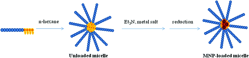 | ||
| Fig. 1 Schematic illustration of the synthetic pathway leading to the formation of the metal (M = Au, Pd) polymer hybrid micellar nanocatalysts. | ||
A similar process was followed for the preparation of small LauMAx-b-AEMAy Pd micellar hybrids in n-hexane.15 In this case 20 mg of LauMA50-b-AEMA9 (∼0.0122 mmol of AEMA units) were dissolved in 5 ml of n-hexane. After complete dissolution of the polymer, 80 μl of triethylamine were added and the resulting solution was mixed with 1.4 mg of Pd(CH3COO)2 (∼0.006 mmol) and left to stir at RT until complete solubilization of the salt. Upon complexation and solubilization the color of the solution changed from white to yellow transparent. Finally, 40 μl of hydrazine monohydrate were added to the solution upon stirring. The reduction of the Pd(II) ions to noble Pd was accompanied by a color change of the solution from yellow transparent to dark brown transparent. Again the solution was further diluted to reach polymer concentrations of 700–0.7 mg L−1, see Table 2. Transmission electron microscopy (TEM) was performed on the Pd MNPs by using a 1010 JEOL microscope (200 kV). The suspension of MNPs was dried on a carbon coated copper grid to allow the TEM investigation.
| Speed/time (rps:sec) |
Au LauMA50-b-AEMA9 (mg l−1) | Pd LauMA50-b-AEMA9 (mg l−1) |
|---|---|---|
| 250:20 |
11400 |
|
| 250:20 |
5570 | |
| 250:20 |
2785 | |
| 250:20 |
1393 | |
| 250:20 |
696 | 700 |
| 200:20 |
696 | 700 |
| 150:20 |
696 | 700 |
| 100:20 |
696 | 700 |
| 50:20 |
696 | 700 |
| 250:20 |
69.6 | 70 |
| 250:20 |
6.96 | 7 |
| 250:20 |
0.696 | 0.7 |
The Au and Pd MNPs prepared at various concentrations using LauMA50-b-AEMA9, were drop casted or spin coated on ∼1 cm2 square pieces of p+ Si(001) at different speeds for 20 s as listed in Table 2.
Before spin coating the p+ Si(001) substrate was cleaned in isopropanol (IPA), acetone (A) and methanol (M), rinsed with de-ionised water (DI H2O) and subsequently dry-baked at 100 °C for 10 min. In general uniform coverage was obtained at speeds >150 rps.
MO NWs were grown using an atmospheric pressure chemical vapour deposition reactor described in detail elsewhere.3 For the growth of β-Ga2O3 NWs, 0.1–0.2 g of Ga (Aldrich, 99.99%) were used while square pieces of Si(001) ∼7 × 7 mm2 coated with the Au or Pd hybrid-MNPs were loaded only a few millimetres away from the Ga inside a quartz boat which was positioned directly above the thermocouple used to measure the heater temperature (TH). After loading, 500 sccm Ar was used to purge for 10 min and then the temperature was ramped to 900 °C under a reduced flow of 100 sccm of Ar at 30 °C min−1. Upon reaching 900 °C the same flow of Ar was maintained for various times between 5–60 min after which the tube was allowed to cool down using the same gas flows during growth. The sample was removed only when the temperature was lower than 100 °C. Similarly ZnO NWs were grown on 8 × 8 mm2 Si(001) with Au or Pd MNPs by reactive vapor transport using 0.2 g Zn under an inert flow of 100 sccm of Ar at 550 °C for 60 min. Finally SnO2 NWs were grown at 800 °C for 60 min using 0.2 g of Sn and an Ar:10% O2 mixture at 0.1 mBar. The morphology of the MO NWs was examined with a TESCAN scanning electron microscope (SEM) and electron beam lithography was carried out using an attached nanolithography system by RAITH. The crystal structure and the phase purity were investigated using a SHIMADZU, XRD-6000 with a Cu–Ka source by performing a scan of θ–2θ in the range between 10–80° and RT photoluminescence (PL) measurements were carried out using excitation of 260 nm.
3. Results and discussion
The single absorbance peak appearing in the UV-vis spectra of the Au MNPs was typically in the range of 520–570 nm due to the characteristic surface plasmon absorption band of the Au NPs.16The UV-vis spectra of the LauMA277-b-AEMA81/Au and the LauMA50-b-AEMA9/Au hybrid micelles recorded in n-hexane, are presented in Fig. 2. As seen from the spectra, the Au MNPs encapsulated within the micellar cores, exhibit size-dependent optical properties, resulting in a shift of the plasmon resonance band from a wavelength of ∼520 nm, corresponding to the LauMA50-b-AEMA9/Au system–smallest micelles, to a wavelength of ∼560 nm, corresponding to the LauMA277-b-AEMA81/Au system–largest micelles. A red shift of the plasmon band from around 520 to 560 nm, assuming a spherical morphology for the NPs, corresponds to an increase in particle diameter from ∼13 to ∼100 nm respectively.17,18
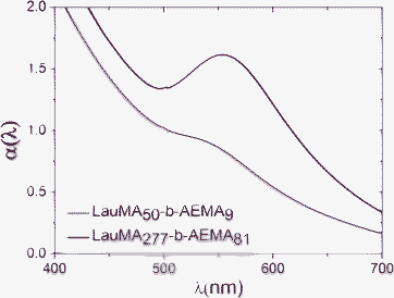 | ||
| Fig. 2 Absorption spectra of Au-MNPs recorded in n-hexane (i) LauMA50-b-AEMA9/Au; lower trace and (ii) LauMA277-b-AEMA81/Au; top trace. | ||
In the case of the Pd-containing nanohybrids, TEM was employed for determining the size of the Pd MNPs incorporated inside the micellar cores of the (i) LauMA277-b-AEMA81, (ii) LauMA120-b-AEMA67 and (iii) LauMA50-b-AEMA9 structures. A TEM image of the medium sized Pd MNPs corresponding to LauMA120-b-AEMA67/Pd is shown in Fig. 3. In all cases, the Pd NPs are characterized by a spherical morphology and have a narrow size distribution and mean diameters of 2.3 ± 0.3, 8.2 ± 1.7 and 18.6 ± 4.5 nm for the LauMA50-b-AEMA9/Pd, LauMA120-b-AEMA67/Pd and LauMA277-b-AEMA81/Pd systems respectively.
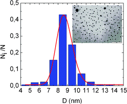 | ||
| Fig. 3 TEM image of the LauMA120-b-AEMA67 Pd MNPs and statistical distribution of diameters. | ||
Before we consider the growth of the Ga2O3 NWs on Si(001) using the Au and Pd hybrid MNPs, it is instructive to point out that Ga2O3 NWs with average diameters of ∼50 nm and lengths of several tens of micrometres shown in Fig. 4(a) were obtained using a thin layer of 0.7 nm Au which was deposited by evaporation on Si(001). These exhibited intense peaks in the XRD corresponding to the monoclinic crystal structure of β-Ga2O3 as shown in Fig. 4(b) while their PL was also intense, broad and centered at 2.3 eV due to crystal defect and/or surface states located energetically in the upper half of the energy band-gap.19 A high yield, uniform distribution of randomly oriented β-Ga2O3 NWs was reproducibly obtained in this way. However, shorter β-Ga2O3 NWs with an average diameter of ∼100 nm were obtained using a high density of 17900 mg l−1 of LauMA277-b-AEMA81 Au MNPs which were drop casted onto Si(001) as shown in Fig. 5 (a). In this case the β-Ga2O3 NWs have maximum lengths of 5 μm and one may observe particles on their ends. The β-Ga2O3 NWs form a characteristic network which extended over several hundreds of μm and had a concentric-ring long range order. Longer and thinner β-Ga2O3 NWs were observed on the periphery. Here it should be pointed out that the polymer surrounding the Au MNPs undergoes a gradual decomposition during growth. This has been confirmed by thermo-gravimetric measurements under a flow of Ar which showed that the polymer begins to lose weight at 200–300 °C whereas it decomposes at 400 °C.14 The network shown in Fig. 5(a) is due to the high density of polymer on the surface of Si(001) but was not uniform over the entire 7 × 7 mm2 area . A slightly better uniformity of β-Ga2O3 NWs with an average diameter of ∼40 nm and lengths > 10 μm as shown in Fig. 5(b) was obtained using LauMA277-b-AEMA81 Au MNPs with a density of 1790 mg l−1 deposited by drop casting on Si(001), even though the growth time in this case was shorter. These are similar to those obtained on 0.7 nm Au/Si(001) shown in Fig. 4(a) and the smaller diameter is attributed to a suppression in the agglomeration of the Au MNPs.
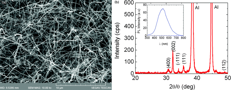 | ||
| Fig. 4 (a) β-Ga2O3 NWs obtained on 0.7 nm Au/p+Si(001); (b) XRD of the Ga2O3 NWs obtained on 0.7 nm Au/Si(001) corresponding to the monoclinic crystal structure of β-Ga2O3. The inset shows the PL. | ||
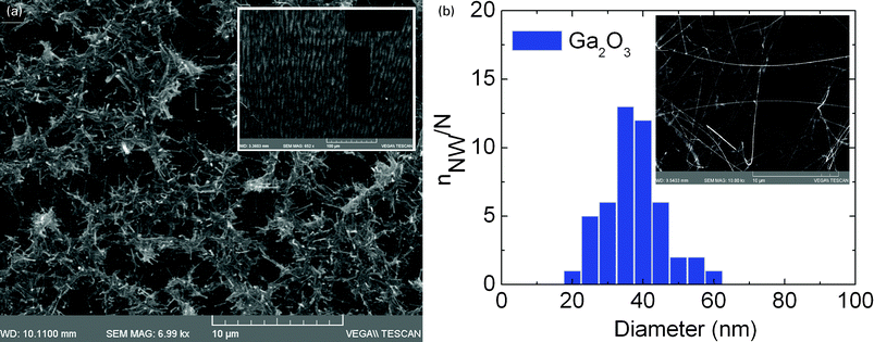 | ||
| Fig. 5 (a) SEM image of β-Ga2O3 NWs grown using LauMA277-b-AEMA81 Au MNPs and high density of 17900 mg l−1; (b) Statistical distribution of β-Ga2O3 NWs diameters shown in the inset, obtained using LauMA277-b-AEMA81 Au MNPs with a density of 1790 mg l−1. | ||
In general drop casting did not give uniform layers even when using low densities of polymer. Uniform layers of the hybrid polymer MNPs extending over the entire 7 × 7 mm2 Si(001) surface were obtained by spin coating. The thickness of the layer in this case is essentially governed by the viscosity of the polymer, angular speed and time. Spin coating was carried out between 5–250 rps for 20 s using different polymer concentrations as listed in Table 2. This also allowed us to perform electron beam lithography (EBL) and remove selectively the hybrid polymer MNPs from the Si(001) surface leaving rectangular areas of plain Si(001). A typical SEM image of a layer of LauMA277-b-AEMA81 Au MNPs that was exposed to a current of 200 pA using a dose of 300 μAs/C and was subsequently developed for 30 s in a 1:1 solution of isopropanol:methyl isobutyl ketone is shown as an inset in Fig. 5(a).
While we obtained only β-Ga2O3 NWs with lengths >10 μm using the largest LauMA277-b-AEMA81 Au MNPs we find that the smallest LauMA50-b-AEMA9 Au MNPs that were spin coated on Si(001), lead to the growth of β-Ga2O3 NWs with a necklace like structure. In particular we obtain β-Ga2O3 NWs with average diameters of 35 nm and lengths of several tens of μm but also short nanostructures emerging from the β-Ga2O3 NWs as shown in Fig. 6 . These are very thin and are very similar to the Ga2O3 NWs obtained with LauMA50-b-AEMA9 based Pd MNPs.
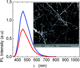 | ||
| Fig. 6 RT PL of necklace like β-Ga2O3 NWs obtained with LauMA50-b-AEMA9 Au MNPs (top trace) and Pd MNPs (lower trace) that were spin coated at 100 and 200 rps respectively for 20 s on Si(001). The inset shows the necklace like β-Ga2O3 NWs obtained using LauMA50-b-AEMA9 (696 mg l−1) Au MNPs. | ||
In addition we have observed β-Ga2O3 NWs decorated with Pd MNPs similar to Au and Ag decorated Ge NWs.13 The β-Ga2O3 NWs decorated with Pd MNPs are attractive for catalysis due to the high thermal stability of β-Ga2O3 and Pd which have high melting points of 1725 °C and 1555 °C respectively.
We do not find any systematic changes in the morphology of these necklace like β-Ga2O3 NWs by varying the spin speed between 50–250 rps or by changing the polymer concentration in the range 696–11400 mg l−1. A reduction in the density of the Au or Pd MNPs by three orders of magnitude i.e. from 696 down to 0.696 mg l−1 lead to the elimination of the necklace like nanostructures. In this case we did not obtain ultra thin β-Ga2O3 NWs but instead observed the formation of β-Ga2O3 rods with diameters exceeding 100 nm and lengths of 1–2 μm. The β-Ga2O3 rods are very similar to those obtained on plain p+ Si(001) which grow via the vapor-solid (VS) mechanism but also similar to β-Ga2O3 rods that were obtained on plain LauMA277-b-AEMA81 polymer on Si(001) without MNPs in their core.
The formation of necklace like or decorated β-Ga2O3 NWs is therefore a direct consequence of the large density of small Au or Pd MNPs but also characteristic of β-Ga2O3 itself since we did not observe similar nanostructures in the case of ZnO or SnO2 NWs. However before considering the latter in more detail we should point out that the RT PL spectra of the necklace like β-Ga2O3 NWs shown in Fig. 6 is less broad and blue shifted compared to the PL shown in Fig. 4(b). This is attributed to quantum confinement effects associated with the thin branched nanostructures that are distributed along the length of the β-Ga2O3 NWs. We believe that if the unique morphologies observed in the case of the Ga2O3 nanowires were attributed to external surface interaction phenomena between the MNPs and the MO NWs, these morphologies would have been also observed in the case where larger MNPs were used. Instead, they have been only observed when the smallest nanoparticle system was employed (LauMA50-b-AEMA9/Pd or Au). A possible explanation for this phenomenon might be the encapsulation of the smallest MNPs within the MO NWs during the growth process. As reported by Chen et al.20 Au MNPs can be encapsulated within Ga2O3 NWs resulting into gold-pea podded Ga2O3 NW structures via thermal annealing of core-shell Au-Ga2O3 nanowires. It is likely that in our case, the encapsulated Au nanoparticles acted as catalytic centers providing branched nanostructures.
The fact that the above-mentioned effect has been only observed in the case of the Ga2O3 system may be attributed to surface energy differences existing between this particular oxide and the other two metal oxides used in the present study i.e. ZnO and SnO2.
ZnO NWs with a hexagonal wurtzite crystal structure and average diameter of 40 nm were obtained using the smallest LauMA50-b-AEMA9 based Au or Pd MNPs as shown in Fig. 7(b). These exhibited emission at 390 nm (∼3.2 eV) depicted in Fig. 7(a) similar to the ZnO NWs which had diameters of 50 nm and were grown using a thin layer of 1.0 nm Au on Si(001). Quantum confinement along r and θ i.e. along the transverse directions, is negligible since the ZnO NWs have diameters which are many tens of nm larger than the size of the MNPs. In addition we do not observe any quantum confinement effects as in the case of β-Ga2O3 NWs since there are no branched nanostructures emerging from the sides of the ZnO NWs that would give rise to confinement in the axial direction. The density of the ZnO NWs decreased upon reducing the density of LauMA50-b-AEMA9 by three orders of magnitude but were found to be similar to those obtained on plain Si(001) since ZnO like β-Ga2O3 NWs grow by a vapor solid (VS) mechanism.
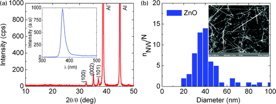 | ||
| Fig. 7 (a) XRD spectrum of the ZnO NWs obtained with LauMA277-b-AEMA81 on Si(001); inset shows PL. (b) Statistical distribution of diameters of ZnO NWs obtained with the smallest of LauMA50-b-AEMA9 MNPs. | ||
From the above it is evident that the diameter of the β-Ga2O3 and ZnO NWs is not governed solely by the size of the micellar MNPs since their growth does not strictly follow the vapor-liquid-solid (VLS) mechanism as in the case of Si NWs where Si enters the Au MNPs leading to their super saturation after which nucleation occurs below the catalysts promoting one dimensional growth. Thin Si NWs with average diameters of 8.0 ± 1 nm10 have been obtained at 550 °C in this way using uniformly sized Au MNPs with diameters of 8.0 ± 0.6 nm derived from PS-b-P2VP block copolymer templates.
The Au and Pd MNPs employed here had a worst case standard deviation of ± 4.5 nm in diameter which is five times smaller than ± 20 nm determined for the MO NWs shown above. The latter is consistent with the range of ZnO NW diameters obtained by blending PS-b-P4VP and PS-b-PAA copolymer micelles.11,12 However it is difficult to account for the difference in the diameter and deviation of the MNPs and MO NWs since this requires MNPs that are well isolated and consequently a very low density on the Si(001) surface which permits the growth of MO NWs on the bare Si(001) surface without any catalyst via the vapor-solid (VS) mechanism. As a consequence one cannot isolate particle mediated from self-catalyzed mechanisms and make meaningful interpretations.
In an attempt to circumvent these difficulties associated with ZnO and β-Ga2O3 NWs we have also considered the growth of SnO2 NWs, using hybrid polymer-MNPs, which do not grow on plain Si(001) by the VS mechanism. A very high yield, uniform distribution of SnO2 NWs with average diameter of ∼50 nm and lengths >10 μm was obtained on 1 nm Au layers deposited on Si(001) as shown in Fig. 8(a) which appeared as a compact white layer. Selective area growth over 80 μm × 80 μm squares of 1 nm thick Au prepared by electron beam lithography is also shown as an inset in Fig. 8(a) from which it is clear that SnO2 NWs do not grow on plain Si(001). Interestingly the yield of the SnO2 NWs grown using the LauMA50-b-AEMA9 Au MNPs/Si(001) was considerably smaller and did not appear as a compact white layer. The density of the SnO2 NWs in this case was significantly smaller and a typical image of the SnO2 NWs grown on the LauMA50-b-AEMA9 Au MNPs/Si(001) is shown in Fig. 8(b). One may observe the formation of intricate, two dimensional networks of SnO2 NWs on the Si(001) surface shown in the inset of Fig. 8(b) and free standing SnO2 NWs emerging at certain junctions of this network. The average diameter of the SnO2 NWs is ∼35 nm which is smaller than 50 nm obtained on 1.0 nm Au/Si(001) but larger than the diameter of the LauMA50-b-AEMA9 Au MNPs estimated to be ∼10 nm. The statistical distribution of the diameters obtained with the LauMA50-b-AEMA9 Pd MNPs is shown in Fig. 9 while we did not observe any necklace like structures as in the case of β-Ga2O3 NWs. This is a significantly better type of nanowire to consider in order to gain a more detailed understanding of the exact growth mechanisms and relation between the diameters of the MNPs and MO NWs to be investigated in the future.
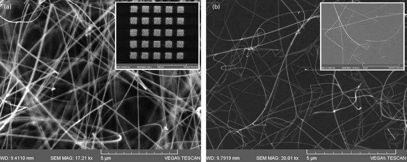 | ||
| Fig. 8 (a) SEM images of free standing SnO2 NWs obtained on 1.0 nm Au/Si(001); inset shows selective area growth on 80 × 80 μm 1 nm thick Au fabricated by EBL on Si(001); (b) SnO2 NWs grown with LauMA50-b-AEMA9 Au MNPs; inset shows intricate network of SnO2 NWs on the surface of Si(001). | ||
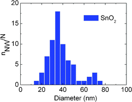 | ||
| Fig. 9 Statistical distribution of SnO2 NW diameters, grown on Si(001) with LauMA50-b-AEMA9 Pd MNPs. | ||
4. Conclusions
ZnO, β-Ga2O3 and SnO2 NWs have been grown by reactive vapor transport on Si(001) using hybrid polymethacrylate based Au and Pd MNPs having diameters as small as 2.3 ± 0.3 nm. β-Ga2O3 NWs with diameters of 40 nm and lengths greater than 10 μm were obtained with the largest MNPs which exhibited a broad symmetric PL spectrum with a maximum at 2.3 eV similar to those obtained by using a 1 nm Au layer on Si(001). Smaller Au or Pd MNPs lead to the formation of necklace like β-Ga2O3 NWs which exhibited blue shifted PL at 2.8 eV attributed to quantum confinement. A suppression of these nanostructures occurred by reducing the density of the smallest MNPs but rod-like β-Ga2O3 NWs were obtained by the vapor-solid mechanism hindering the growth of thin β-Ga2O3 NWs. No necklace like nanostructures were obtained in the case of ZnO or SnO2 NWs which had average diameters of 40 nm by using the smallest MNPs. The diameter of all the MO NWs is not governed solely by the size of the micellar MNPs since the hybrid polymer MNPs tend to coalesce at elevated temperatures while self-catalyzed mechanisms also come into play upon reducing the density of MNPs. Polymethacrylate coated MNPs are promising for the directed self-assembly of NWs since they may be patterned directly using conventional lithography.References
- Y. Cui and C. M. Lieber, Functional nanoscale electronic devices assembled using silicon nanowire building blocks, Science, 2001, 291, 851 CAS.
- Y. Wu, R. Fan and P. Yang, Block-by-block growth of single-crystalline Si/SiGe superlattice nanowires, Nano Lett., 2002, 2, 83 CAS.
- M. Zervos and A. Othonos, Gallium hydride vapor phase epitaxy of GaN nanowires, Nanoscale Res. Lett., 2011, 6, 262 CAS.
- Z. L. Wang, Nanostructures of ZnO, Mater. Today, 2004, 7, 26 CAS.
- D. Tsokou, M. Zervos and A. Othonos, Ultrafast spectroscopy of In2O3 nanowires grown by the vapor-liquid-solid method, J. Appl. Phys., 2009, 106, 084307 Search PubMed.
- P. Papageorgiou, M. Zervos and A. Othonos, An investigation into the conversion of In2O3 to InN nanowires, Nanoscale Res. Lett., 2011, 6, 311 CAS.
- A. Othonos, M. Zervos and C. Christofides, Carrier dynamics in β-Ga2O3 nanowires, J. Appl. Phys., 2010, 108, 124302 Search PubMed.
- A. Othonos, M. Zervos and D. Tsokkou, Tin oxide nanowires Influence of trap states on ultra fast carrier relaxation, Nanoscale Res. Lett., 2009, 4, 828 CAS.
- J. M. Campelo, D. Luna, R. Luque, J. M. Marinas and A. Romero, Sustainable preparation of supported metal nanoparticles and their applications in catalysis, ChemSusChem, 2009, 2, 18 CAS.
- J. Q. Lu and S. S. Yi, Uniformly sized gold nanoparticles derived from PS-b-P2VP block copolymer templates for the controllable synthesis of si nanowires, Langmuir, 2006, 22, 3951 CAS.
- W. H. Wang, J. H. Choi, T. H. Kim, J. Sung, J. M. Myong, D. G. Choi, B. H. Sohn, S. S. Lee, D. H. Kim and C. Park, Control of the area density of vertically grown ZnO nanowires by blending PS-b-P4VP and PS-b-PAA copolymer micelles, Chem. Mater., 2008, 20, 6041 Search PubMed.
- G. S. Doerk, C. Dhong, C. Politi, I. Laboriante, C. Carraro and R. Maboudian, Micellar block copolymer templated galvanic displacement for epitaxial nanowire device integration, J. Mater. Chem., 2011, 21, 8807 CAS.
- J. Zhang, Y. Gao, T. Hanrath, B. A. Korgel and J. M. Buriak, Block copolymer mediated deposition of metal nanoparticles on Ge nanowires, Chem. Commun., 2007, 1438 CAS.
- M. Demetriou and T. Krasia, Synthesis and characterization of well-defined block and statistical copolymers based on lauryl methacrylate and 2-(acetoacetoxy)ethyl methacrylate employing RAFT controlled radical polymerization, J. Polym. Sci., Part A: Polym. Chem., 2008, 46, 5442 CAS.
- K. Iliopoulos, G. Chatzikyriakos, M. Demetriou, T. Krasia-Christoforou and S. Couris, Preparation and nonlinear optical response of novel palladium-containing micellar nanohybrids, Opt. Mater., 2011, 33, 1342 CAS.
- S. Md. Nasir and H. Nur, Gold nanoparticles embedded on the surface of polyvinyl alcohol layer, J. Fundam. Sci., 2008, 4, 245 Search PubMed.
- M. Q. Zhu, M. Q. Wang, L. Q. Exarhos, G. J. Li, Li-Qiong Wang and J. A. D. Q Gregor, Thermosensitive Au nanoparticles, J. Am. Chem. Soc., 2004, 126, 2656–2657 CAS.
- F. Toderas, M. Baia, D. Maniu and S. Astilean, Tuning the plasmon resonances of gold nanoparticles by controlling their size and shape, J. Optoelectron. Adv. Mater., 2008, 10, 2282–2284 CAS.
- P. H. Chen, C. H. Hsieh, S. Y. Chen, C. H. Wu, Yi. J. Wu, L. J. Chou and L. J. Chen, Direct observation of Au/Ga2O3 peapodded nanowires and their plasmonic behaviors, Nano Lett., 2010, 10, 3267 CAS.
| This journal is © The Royal Society of Chemistry 2012 |