Direct growth of nanographene films by surface wave plasma chemical vapor deposition and their application in photovoltaic devices†
Golap
Kalita
*,
Madhu Sudan
Kayastha
,
Hideo
Uchida
,
Koichi
Wakita
and
Masayoshi
Umeno
Department of Electronics and Information Engineering, Chubu University, 1200, Matsumoto-cho, Kasugai-shi, 487-8501, Japan. E-mail: golapkalita@yahoo.co.in
First published on 8th March 2012
Abstract
Here, we report direct synthesis of nanographene films on silicon (n-Si) and glass (SiO2) substrates by microwave assisted surface wave plasma (MW-SWP) chemical vapor deposition (CVD) and their application in photovoltaic devices. The technique is a metal catalyst free, rapid growth process and the film can be deposited on different substrates; thus simplifying the synthesis process for various device applications. The directly grown graphene film consists of triangular shaped nanographene domains with sizes of 80–100 nm in length. The nanographene domains interconnect to form a continuous film which shows metallic characteristics. A Schottky junction based photovoltaic device is fabricated with directly grown nanographene film on n-Si and a conversion efficiency of 2.1% is achieved. This finding shows that a transparent nanographene film can be deposited on different substrates and can be integrated for various devices.
1. Introduction
Graphene is a perfect two-dimensional (2D) carbon sheet with hexagonal structures similar to benzene rings and is the basic building block of graphite, fullerene, and carbon nanotubes (CNTs). Since the discovery of graphene in 2004,1 there has been an intense focus on graphene based materials, owing to their interesting electrical and optical properties for electronic device application.2–5 There has been a lot of effort made to exploit the outstanding electrical, optical and mechanical properties of graphene for fabrication of transparent electrodes.6–8 The synthesis of graphene has been achieved by various approaches, such as by thermal CVD on metal sheets and by the chemical reduction of graphene oxide which have been shown to be most suitable as transparent electrodes.9–14 However thermal CVD graphene synthesis involves a metal catalytic layer and very high deposition temperature, typically around 1000 °C.9,15 A catalyst free direct growth process at low-temperature can be far more advantageous for device applications. This can pave the way for direct integration of the graphene based materials with other suitable materials for device applications.Lot of studies has been carried out on fabrication of amorphous carbon (a-C) and Si heterojunction diodes and photovoltaic devices.16–18 However, lack of ability to control the electrical and structural properties of a-C is a big disadvantage in the fabrication of heterojunction devices. Recent studies have reported the fabrication of CNT/Si heterojunction photovoltaic devices.19,20 In a bulk CNT/Si junction, there can be two types of heterostructures (Schottky and p–n heterojunction) as both metallic and semiconducting nanotubes coexist. Fabrication of a Schottky junction with a transferred CVD and mechanically exfoliated graphene on Si has also been demonstrated.21,22 However, fabrication of large area solar cells with transferred graphene on brittle Si can have many disadvantages. There can be inhomogeneous contact formation, breaking of the graphene film during the transfer process and trapping of impurities at the interface. These problems can only be overcome with the direct growth of the graphene film for integration into a photovoltaic device.
In this communication, we demonstrate the synthesis of nanographene films on n-Si and SiO2 substrates by the MW-SWP CVD technique and the fabrication of a photovoltaic device. The directly grown graphene film consists of triangular shaped nanographene domains with sizes of 80–100 nm in length. The nanographene domains interconnect to form a continuous film which shows metallic behavior.
2. Experimental
2.1 Synthesis of the graphene films and characterization
Nanographene films were deposited on n-Si (10 Ω cm) and SiO2 substrates by using a MW-SWP-CVD technique (schematic figure in the ESI†). In the MW-SWP-CVD system a hollow quartz plate is used for plasma generation. It has been reported that by using a hollow plate plasma formation can be started-up smoothly without any density jump and the plasma density is two times higher than that of a flat plate. High density surface wave plasma can be generated in the meter scale and large area deposition can be achieved at a very fast rate.23 For the deposition of the graphene film a gas mixture of C2H2 and Ar with flow rates of 10 and 200 standard cubic centimeters per minute (sccm), respectively were used for all experiments. Deposition was carried out on the substrates without any pretreatment at a gas composition pressure of 45 Pa for a duration of 70–120 s. The power of the microwave used for the deposition was 1.2 kW, having a negligible amount of fluctuation.The nanographene films were characterized with Raman spectroscopy having a laser excitation energy of 532 nm in a NRS 300 laser Raman spectrometer, scanning electron microscopy (SEM) using a FESEM Hitachi S-4300, high-resolution transmission electron microscope (HRTEM) JEOL:JEM-2100F operated at 200 kV and atomic force microscopy (AFM) using a OLS3500/SFT-3500. Optical transmittance characterization of the graphene sheets on glass were carried out with UV-VIS-NIR on a JASCO-V570 spectrophotometer. Sheet resistance measurements were carried out using the four probe technique.
2.2 Device fabrication and characterization
For Au/graphene/Au device fabrication, gold electrodes were deposited by sputtering on the directly grown graphene film on a SiO2 substrate. Current density–voltage (J–V) measurements were carried out without illumination in different bias voltages. Schottky junction photovoltaic devices were fabricated using n-Si (111) substrates having a resistivity of 10 Ω cm. Prior to deposition of the graphene films, the n-Si substrates were cleaned with acetone and methanol solution. A SiO2 layer with a thickness of 200 nm was deposited using a device mask of 0.2 cm2. A patterned device area nanographene film was created by direct deposition on the n-Si substrate. The top gold electrode was deposited by the ion sputtering technique (E-1030 ION SPUTTER). The J–V characteristic of the devices were measured at room temperature (25 °C) using a JASCO SS-200 W solar simulator in the dark and under air mass (AM) 1.5 simulated solar radiation.3. Results and discussion
Fig. 1(a) presents the Raman studies on the carbon films deposited on glass (SiO2) at different substrates temperatures. The Raman spectra show a strong and sharp graphitic G band at 1568 cm−1, representing the crystalline sp2 structure of the nanographene domains. A disorder induced D peak is also observed at 1339 cm−1; the high intensity of the D peak originates from either the small crystallite sizes or an abundance of edges in the nanographene structures. Three other peaks are observed at 2669, 2915, and 3214 cm−1 corresponding to 2D, G + D and 2G second-order Raman peaks, respectively. The presence of a distinct 2D peak is in good agreement with graphene structures formed in deposited films.24–26 Similarly, Fig. 1(b) shows the Raman studies of the carbon films deposited on Si substrates, and shows D, G and 2D peaks at around 1341, 1566 and 2665 cm−1, respectively. The Raman studies show that the structure of the nanographene is similar and independent of the Si or SiO2 substrates. The graphene film deposited at 560 °C shows a greatly enhanced 2D peak, and a more suppressed D + G peak compared to those of the low temperature deposited films; indicating a more ordered graphene structure. The studies show that the CVD process can be used for direct deposition of nanographene films on different substrates without using a metal catalytic layer. In the growth mechanism, a carbon radical formed with hydrogen termination in the microwave plasma and plays a key role in the nucleation and growth process in the metal free substrates. The carbon radical from the plasma absorbs onto the substrate and bonds to other such radicals by a diffusion process to form sp2 carbon.25,27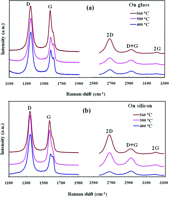 | ||
| Fig. 1 Raman spectra of the nanographene films deposited at 400, 500 and 560 °C on (a) glass (SiO2) and (b) n-Si substrates. | ||
The nanographene film deposited at 560 °C has the best structural order, as observed in the Raman spectra, and is used here for further studies and device fabrication. Fig. 2(a) shows an SEM image of the deposited nanographene showing continuous film formation. No other information can be obtained from the SEM studies; hence the domain structures were studied by AFM. Fig. 2(b) shows an AFM image of graphene grown on a Si substrate and shows the triangle shaped nanographene particles. The sides of the nanographene particles are of the order of 80–100 nm. It was observed that the triangle shaped nanographene domains are independent of the substrate and have similar structures on both the Si and SiO2 substrates. The triangular nanographene domains interconnect to form a continuous path for the flow of electrons as shown in the Fig. 2(c).
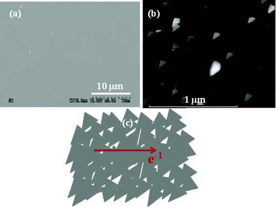 | ||
| Fig. 2 (a) An SEM image of the deposited continuous nanographene film. (b) AFM image of nanographene grown on a Si substrate with triangular domain structures (the morphology is similar on a SiO2 substrate). (c) A schematic of the triangular nanographene domain forming a continuous film. | ||
Fig. 3(a) and (b) show TEM images at the edges of the nanographene domains, indicating the formation of few-layered graphene structures. The inter-planar spacing of the graphene is estimated to be 0.345 nm, which again corresponds to the graphite d(002) spacing. The presented graphene layers are of an individual nanographene domain, which overlap with other domains in the deposited films. Hence, the number of graphene layers shown cannot be directly related to the results of transmittance measurements. Fig. 3(c) shows an HRTEM image of a graphene sheet to examine the crystal and atomic packing structure. The image shows a graphitic crystalline structure, though some defects are present in the sp2 hexagonal structures. The inset of Fig. 3(c) shows a fast Fourier transform (FFT) image of the few-layered nanographene, showing a set of hexagonal spots in the diffraction pattern, indicative of hexagonal sp2 carbon. The Raman and TEM studies clearly indicate that the deposited nanographene domain structures are crystalline rather than disordered.
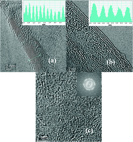 | ||
| Fig. 3 (a) and (b) show transmission electron microscopy (TEM) studies of the edge of a nanographene flakes deposited at 560 °C and show the few-layer graphene structure (inset of the figure: intensity pattern of the few-layer graphene). (c) HRTEM image at the top of the graphene sheet (inset of the figure: Fast Fourier transform (FFT) with a set of hexagonal spot in the diffraction pattern). | ||
The synthesized nanographene films on SiO2 and Si were sufficiently thin to be transparent over the relevant range of wavelengths. Fig. 4(a) presents the transmittance of the nanographene films deposited for different durations in comparison with a standard ITO coated substrate. The transmittance of the graphene film deposited for the shortest duration was 82% at a wavelength of 550 nm. The sheet resistance measurements of the graphene films deposited on glass substrates were carried out with four probe measurements. Fig. 4(b) presents the sheet resistance of the graphene films as a function of transmittance at a wavelength of 550 nm. The sheet resistance of a graphene film with transmittance of 82% at 550 nm wavelength is 6.8 kΩ sq−1; which is better than that reported for reduced graphene oxide and comparable with some of the reported CVD based graphene samples.7,11,25 As the thickness of the deposited graphene film is of a few nanometers, the lateral conductivity will be very high. The greater electrical conductivity of the graphene film would make it possible to retain adequate lateral electrical conductance in a fabricated electronic devices. The I–V characteristics of a graphene film deposited on glass substrates are measured to study the conductivity behavior. A graphene/metal contact device on a glass substrate with a pair of Au electrode was fabricated as shown in Fig. 4(c) for I–V measurements. The corresponding I–V characteristics of the Au/CVD graphene/Au devices are shown in Fig. 4(d), all of which are of linear character. No current saturation was observed for the graphene film devices when a much higher bias voltage (15 V) was applied. The linear form of the I–V curve indicates the metallic behavior of the as-grown nanographene films. The linear I–V curve also indicant good electrical conduction in the interconnected nanographene domains, thereby eliminating hoping conductance due to the presence of nanostructured domains. The measured sheet resistance of the nanographene films, obtained from the slope of the I–V curve (Fig. 4(d)), can be compared with the above mentioned sheet resistance results.25,26 At present, the sheet resistance is quite high, as the synthesized graphene films consist of nanosized domains. To increase the domain size, the deposition of graphene films at a higher temperature has to be studied. Other deposition parameters such as microwave power and gas composition pressure can also play an important role in the graphene structure formation, which will be further investigated.
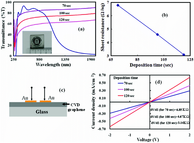 | ||
| Fig. 4 (a) Transmittance of the nanographene films deposited at 560 °C for different durations in comparison to indium tin oxide (inset of the figure: a photograph of nanographene deposited an SiO2 substrate). (b) Sheet resistance of the graphene films against the variation of transmittance at 550 nm. (c) A schematic diagram of the Au/graphene/Au device on glass. (b) J–V characteristics of the fabricated devices with nanographene films deposited for different durations. | ||
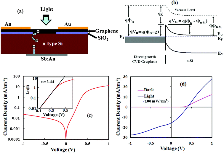
A photovoltaic device was fabricated with the directly grown nanographene film on the n-Si substrate. Fig. 5(a) shows a schematic diagram of the fabricated nanographene/n-Si junction device. The incident light in the device can transmit through the transparent graphene film and get absorbed in the n-Si to generate photo-exciton. Fig. 5(b) shows energy band diagram of the nanographene/n-Si photovoltaic device in thermal equilibrium. Due to the metallic behavior of the graphene film, a Schottky junction can be formed with the n-Si. Previous studies have shown that a transparent graphene sheet forms a Schottky junction with Si, which is favorable in producing a relatively large built-in field (Vbi, 0.55–0.75 V).21 Due to the presence of large built-in field in the graphene/n-Si junction there can be efficient charge separation and transportation. Fig. 5(c) shows a log scale plot of the dark J–V characteristics of the fabricated nanographene/n-Si device. The dark characteristics show that the device has a rectifying diode character with a rectification ratio of 104, which is similar to an ideal diode characteristic. A fitting plot of ln(I)–V in forward bias (inset of Fig. 5(c)) shows a linear character in the range of 0.1–0.37 V having a diode ideality factor (n) of 2.44. Similarly, the series resistance (Rs) of the fabricated device as calculated from the dark measurements is 17.5 Ω. Fig. 5(d) shows the J–V characteristics of the fabricated device under illumination of 100 mW cm−2. The device shows a photovoltaic action with an open circuit voltage (Voc) of 0.41 V, a short circuit current density (Jsc) of 15.6 mA cm−2 and a fill factor (FF) of 33% with power conversion efficiency (η) 2.11%. The Voc of the fabricated device with directly grown nanographene gives the barrier energy, which is consistent with that of a transferred graphene and n-Si junction in the literature.21,22 Photo-excited electrons and holes are generated in the Si substrate, which are separated and collected by virtue of the built-in electric field at the nanographene/n-Si junction. High Jsc is obtained in the device with a better junction formation with direct growth nanographene film on n-Si. The fabricated photovoltaic device shows similar or better performance than that of a transferred graphene/n-Si Schottky junction device.21,22 Further, there is a lot of scope to improve the device performance with proper selection of electrode materials for ohmic contacts and enhancing the quality of the deposited film, which will be further investigated. Moreover, the direct growth nanographene structures on Si or SiO2 can be used for many other applications.
 | ||
| Fig. 5 (a) Schematic diagram of the fabricated nanographene/n-Si Schottky junction device. (b) The energy-band diagram of the fabricated device; showing the formation of a potential barrier at the interface. (c) J–V curve as a log plot under dark conditions (inset of the figure, a fitting plot of ln(I)–V in forward bias). (d) J–V characteristics in the dark and under illumination of 100 mW cm−2. | ||
4. Conclusions
In conclusion, low temperature direct growth of nanographene films on Si and SiO2 substrates was achieved by MW-SWP-CVD. The method is metal catalyst free and the growth process is rapid (deposition time 70 s), and thus is more simple for various device applications. The directly grown graphene films consisted of triangular shaped nanographene domains with sizes of 80–100 nm in length. The nanographene domains interconnected to form a continuous film which showed metallic characteristics. A Schottky junction diode fabricated with the directly grown nanographene film on n-Si showed very good rectification and diode characteristics. Under illumination with light, the fabricated Schottky junction photovoltaic device shows Voc 0.41 V, Jsc 15.6 mA cm−2 and FF 33% with a power conversion efficiency (η) of 2.1%.Acknowledgements
The corresponding author would like to thank the Japan Society for the promotion of Science (JSPS) for the fellowship and financial support.References
- K. S. Novoselov, A. K. Geim, S. V. Morozov, D. Jiang, Y. Zhang, S. V. Dubonos, I. V. Grigorieva and A. A. Firsov, Science, 2004, 306, 666–669 CrossRef CAS.
- C. Berger, Z. Song, T. Li, X. Li, A. Y. Ogbazghi, R. Feng, Z. Dai, A. N. Marchenkov, E. H. Conrad, P. N. First and W. A. Heer, J. Phys. Chem. B, 2004, 108, 19912 CrossRef CAS.
- Y. Zhang, Y. W. Tan, H. L. Stormer and P. Kim, Nature, 2005, 438, 201–204 CrossRef CAS.
- K. S. Novoselov, A. K. Geim, S. V. Morozov, D. Jiang, M. I. Katsnelson, I. V. Grigorieva, S. V. Dubonos and A. A. Firsov, Nature, 2005, 438, 197–201 CrossRef CAS.
- S. Stankovich, D. A. Dikin, G. H. B. Dommett, K. M. Kohlhaas, E. J. Zimney, E. A. Stach, R. D. Piner, S. T. Nguyen and R. S. Ruoff, Nature, 2006, 442, 282–286 CrossRef CAS.
- G. Eda, G. Fanchini and M. Chhowalla, Nat. Nanotechnol., 2008, 3, 270–274 CrossRef CAS.
- K. S. Kim, Y. Zhao, H. Jang, S. Y. Lee, J. M. Kim, K. S. Kim, J. Ahn, H. P. Kim, J. Y. Choi and B. H. Hong, Nature, 2009, 457, 706–710 CrossRef CAS.
- X. S. Li, W. W. Cai, J. H. An, S. Kim, J. Nah, D. X. Yang, R. Piner, A. Velamakanni, I. Jung, E. Tutuc, S. K. Banerjee, L. Colombo and R. S. Ruoff, Science, 2009, 324, 1312–1314 CrossRef CAS.
- S. Bae, H. K. Kim, Y. Lee, X. Xu, J. Park, Y. Zheng, J. Balakrishnan, D. Im, T. Lei, Y. Song, Y. Kim, K. Kim, B. Ozyimaz, J. Ahn, B. Hong and S. Iijima, Nat. Nanotechnol., 2010, 5, 574–578 CrossRef CAS.
- A. Reina, X. Jia, H. John, D. Nezich, H. Son, V. Bulovic, M. S. Dresselhaus and J. Kong, Nano Lett., 2009, 9, 30–35 CrossRef CAS.
- X. Wang, L. Zhi and K. Mullen, Nano Lett., 2008, 8, 323–327 CrossRef CAS.
- J. Wu, H. A. Becerril, Z. Bao, Z. Liu, Y. Chen and P. Peumans, Appl. Phys. Lett., 2008, 92, 263302 CrossRef.
- G. Kalita, M. Masahiro, H. Uchida, K. Wakita and M. Umeno, J. Mater. Chem., 2010, 20, 9713–9717 RSC.
- Y. Wang, S. W. Tong, X. F. Xu, B. Özyilmaz and K. P. Loh, Adv. Mater., 2011, 23, 1514–1518 CrossRef CAS.
- Y. Lee, S. Bae, H. Jang, S. Jang, S. E. Zhu, S. H. Sim, Y. Song, B. H. Hong and J. H. Ahn, Nano Lett., 2010, 10, 490–493 CrossRef CAS.
- H. A. Yu, Y. Kaneko, S. Yoshimura and S. Otani, Appl. Phys. Lett., 1996, 68, 547 CrossRef CAS.
- K. Mukhopadhyay, I. Mukhopadhyay, M. Sharon, T. Soga and M. Umeno, Carbon, 1997, 35, 863–864 CrossRef CAS.
- M. Ma, Q. Xue, H. Chen, X. Zhou, D. Xia, C. Lv and J. Xie, Appl. Phys. Lett., 2010, 97, 061902 CrossRef.
- J. Q. Wei, Y. Jia, Q. K. Shu, Z. Y. Gu, K. L. Wang, D. M. Zhuang, G. Zhang, Z. C. Wang, J. B. Luo, A. Y. Cao and D. H. Wu, Nano Lett., 2007, 7, 2317–2321 CrossRef CAS.
- Y. Jia, A. Cao, X. Bai, Z. Li, L. Zhang, N. Guo, J. Wei, K. Wang, H. Zhu, D. Wu and P. M. Ajayan, Nano Lett., 2011, 11, 1901–1905 CrossRef CAS.
- X. Li, H. Zhu, K. Wang, A. Cao, J. Wei, C. Li, Y. Jia, Z. Li, X. Li and D. Wu, Adv. Mater., 2010, 22, 2743–2748 CrossRef CAS.
- C. C. Chen, M. Aykol, C. C. Chang, A. F. J. Levi and S. B. Cronin, Nano Lett., 2011, 11, 1863–1867 CrossRef CAS.
- G. Zhong, M. Tachiki, H. Umezawa, T. Fujisaki, H. Kawarada and I. Ohdomari, Chem. Vap. Deposition, 2004, 10, 125–128 CrossRef CAS.
- J. Kim, M. Ishihara, Y. Koga, K. Tsugawa, M. Hasegawa and S. Iijima, Appl. Phys. Lett., 2011, 98, 091502 CrossRef.
- L. Zhang, Z. Shi, Y. Wang, R. Yang, D. Shi and G. Zhang, Nano Res., 2011, 4, 315–321 CrossRef CAS.
- K. B. Kim, C. M. Lee and J. Choi, J. Phys. Chem. C, 2011, 115, 14488–14493 CAS.
- G. Kalita, K. Wakita and M. Umneo, RSC Adv., 2012 10.1039/C2RA00648K.
Footnote |
| † Electronic supplementary information (ESI) available. See DOI: 10.1039/c2ra01024k |
| This journal is © The Royal Society of Chemistry 2012 |