Highly sensitive H2S sensor based on template-synthesized CuO nanowires
Xiaopeng
Li
a,
Ying
Wang
b,
Yu
Lei
b and
Zhiyong
Gu
*a
aDepartment of Chemical Engineering, University of Massachusetts-Lowell, Massachusetts, United States. E-mail: Zhiyong_Gu@uml.edu; Fax: +01 978 934 3047; Tel: +01 978 934 3540
bDepartment of Chemical, Materials and Biomolecular Engineering, University of Connecticut, Storrs, Connecticut, United States
First published on 20th January 2012
Abstract
A sensor device featuring massive aligned CuO nanowires has been fabricated for H2S detection. Metallic copper (Cu) nanowires were first synthesized by a template-assisted electrodeposition method. Dielectrophoresis (DEP) and thermal oxidation were then used to assemble and functionalize/oxidize the nanowires. Topology of the CuO nanowires showed rugged surfaces on the nanowires. H2S sensing properties were characterized by conducting experiments with varying influential factors, including concentration levels from 10 to 1000 ppb and working temperatures from 25 to 420 °C. The CuO nanowire sensor showed good response and repeatability upon H2S exposure with a detection limit of 2.5 ppb and a linear response ranging from 10 ppb to 100 ppb. In addition, the study of temperature influence revealed that the highest response was achieved at 180 °C. Furthermore, with increased working temperature, the CuO nanowire sensor had shorter response and recovery times. An interesting two-stage response was discovered for this CuO nanowire sensor responding to H2S exposure, indicating that two competing reactions existed on the CuO surface.
Introduction
Hydrogen sulfide has very often been referred to as one of the most common toxic pollutants, and has received great interest over the past decades with raised awareness and concerns over air quality and health issues.1,2 Hydrogen sulfide is a colorless, flammable and noxious gas with the formula H2S. It is abundant in nature, and forms in volcanic eruptions and anaerobic digestion and occurs in natural gas. The predominant sources of H2S generation in modern society are combustion of fossil fuels and industrial processes such as paper making,3 crude oil refining4 and food processing.5 H2S can be hazardous to both the environment and the human body. H2S emission into the air and water system may lead to serious damage because it is corrosive, and could also change into sulfur dioxide and sulfuric acid, as the main contributors of acid rain. Occupational harmful levels of hydrogen sulfide exposure are less than 10 ppm,6 and the harmful effects to the human body include irritation to the inspiration system, dysfunction of the nervous system and even loss of consciousness.7 Therefore, the pressing need to detect or monitor trace amounts of H2S has drawn tremendous attention from both academia and industry.Currently, semiconducting metal oxide chemiresistive sensors are a major type of sensor to achieve this goal, and materials such as SnO2,8 In2O3,9 CuO,10 WO3,11 ZnO,12etc., have been intensively studied and used for this purpose. Among them, CuO materials are especially favored in H2S detection due to the p-type semiconducting properties13 and unique surface chemistry with H2S.14 In recent years, with the emerging appearance of nanomaterials, new innovations have been seen in sensor technology. High surface-to-volume ratio nanostructures such as nanofibers,15 nanoflowers,16 nanoflakes17 and nanowires18 have been synthesized and studied. However, out of the limited publications on CuO nanomaterials for H2S sensing, only a few of them were focused on nanowire structure, which is more favoured for device assembly and integration. More importantly, prior works either had experiments only conducted at sub-ppm level or had a detection limit not low enough to alert early stage H2S detection at a few ppb level.
In this article, we present a novel, highly sensitive H2S sensor that features template synthesized CuO nanowires as the functional sensing component and an enhanced sensor assembling process. Nanowires were first prepared in their metallic form and then thermally oxidized to their oxide form to bring out the chemiresistive nature for sensing. During this transition, significant surface morphology change was observed. Sensor chips were fabricated using dielectrophoretic (DEP) assembly to integrate the nanowires, and the sensing performance towards exposure of H2S was measured in a dynamic testing system. An interesting two-stage sensing response of the CuO nanowires to H2S was discovered, and both temperature influence and H2S concentration were taken into account to study the sensor response variations. Finally, the sensor response from this CuO nanowire sensor was also compared with that of a SnO2 nanowire sensor.
Experimental
Nanowire synthesis
The nanowire growth occurred inside the hollow structures of a polycarbonate (PC) membrane (Whatman) through an electrochemical process. First, the back side of the PC membrane was coated with a thin layer of silver to promote electrical contact with the copper plate which served as the cathode. The front side of the membrane was placed in a glass tube with an O-ring, and later the glass tube was filled with copper plating solution (Copper U Bath RTU, Technic) to form a plating bath. A constant current of 2 mA was generated by a potentiostat (VersaSTAT 3, Princeton Applied Research) and applied through a platinum electrode and the copper plate. Upon completion of the electrodeposition, the membrane was dissolved in dichloromethane and the nanowires were detached from the silver layer and dispersed into solvent. Then, the as-fabricated pure copper nanowires had an orange-red color and were rinsed and finally stored in ethanol.Sensor fabrication
Fig. 1a depicts the main steps of the sensor fabrication process. Dielectrophoretic assembly was adopted here to align nanowires and form contacts with microelectrodes, which are commercially available from Heraeus (MSP332). First, about 0.15 ml of Cu nanowire suspension was transferred to the substrate electrodes under a non-uniform electric field, generated by applying a sine wave AC voltage to the electrodes. Under the influence of dielectrophoretic force, the nanowires were oriented to the direction vertically to these interdigitated electrodes. After the liquid media (ethanol) completely evaporated, the nanowires were trapped between the gaps of electrodes, bridging them as electrical paths. Hence, the surface of our sensor platform was covered by a thin layer of aligned Cu nanowires, which had a dark orange color (Fig. 1b). The gas sensing capability was activated by conversion of the metallic nanowires to chemiresistive metal oxide nanowires which are, in this case, CuO nanowires. Thereafter, the chip with nanowires was placed in a tube furnace and annealed at ∼700 °C for more than 4 h for complete thermal oxidation. The oxidized nanowires on the substrate (Fig. 1c) had the characteristic black color of CuO. Finally, this sensor chip was connected to an external power supply for the control of working temperature and a sampling device for data acquisition, ready for the sensing test.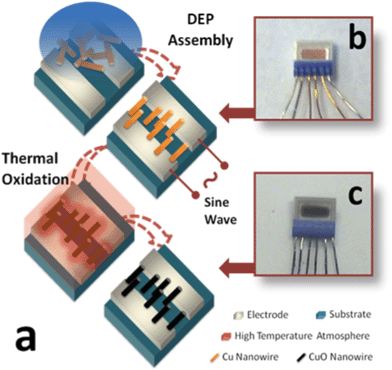 | ||
| Fig. 1 (a) A diagram of sensor chip fabrication procedure; (b) top view of sensor chip before oxidation; (c) top view of same sensor chip after oxidation | ||
Morphology and elementary characterization of nanowires
The surface morphology of nanowires was characterized using a JEOL JSM-7401F field emission scanning electron microscope (FE-SEM) before and after oxidation. To perform the characterization, Cu nanowires were dispersed on a piece of Si wafer for SEM imaging; the images of CuO nanowires were taken by mounting the sensor chip onto a specimen stub and placing it directly into the FE-SEM. The X-ray diffraction (XRD) pattern of the CuO nanowires was obtained using an Oxford diffraction Xcalibur PX Ultra with ONYX detector for crystal phase study.The sensor chip was sealed into a home-made 5 cm3 glass chamber with gas inlet and outlet. The sensor circuit was subjected to a fixed 0.1 V DC, and the current reading was instantly measured by a CHI-601C electrochemical analyzer (CH Instruments Inc., Austin, TX, USA) at a sampling rate of one point per second. Dry air was used as the carrier gas to obtain H2S mixtures with concentrations ranging from 10 ppb to 1000 ppb, which was regulated by a computer-controlled gas mixing system (S-4000, Environics Inc., Tolland, CT, USA). All experiments were carried out using a flow rate at 1.8 L min−1. In a typical testing cycle, a stable baseline was first obtained by flashing dry air through the chamber for one hour before experiments, then the sample was exposed to H2S for 10 min, followed by dry air purging of 15 min to allow the sensor to recover. The electric resistance of the sensor was calculated by applying Ohm's law (R = V/I). Sensor response equals the normalized resistance change and is defined as ΔR/R0 = [(R − R0)/R0], where R0 is the initial electrical resistance of the sensor in dry air and R is the measured real-time resistance upon exposure to H2S or air.
Results and discussion
Thermal oxidation
The as-fabricated copper nanowires were examined first under SEM (Fig. 2a), and had a typical dimension of 5–6 μm in length and 50–70 nm in diameter. Since the growth of the nanowires through the electrodeposition process occurred in the cylindrical hollow structures of the membrane, and was confined by the side-walls, relatively smooth surfaces were observed for the copper nanowires, as shown in Fig. 2b. In contrast, the same batch of nanowires had a dramatically different surface condition when converted into copper oxide, as the rugged surfaces show in Fig. 2c. The formation of irregular bumpy surfaces on the CuO nanowires are attributed to the growth and relief of stress generated during oxidation. More specifically, the stress may come from recrystallization, non-stoichiometric growth19 and the volume difference between the metallic form and metal oxide form under the influence of diffused oxygen atoms into the nanowires. It is also during the oxidation process that the natural non-stoichiometric defects altered the electrical properties of the material, causing a metal deficient p-type semiconducting behavior.20 This oxidation activated the nanowires to be capable of gas sensing. It should be noted that this surface morphology change actually increased the surface area of these nanowires in comparison with that of the copper nanowires, which is in favor of surface chemistry-based gas sensing.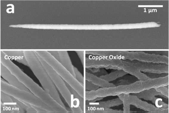 | ||
| Fig. 2 (a) SEM image of a single Cu nanowire; (b) surface morphology of Cu nanowires before oxidation; (c) surface morphology of nanowires after oxidation (CuO nanowires). | ||
In addition, the X-ray diffraction pattern of the oxidized nanowires was obtained. This crystallographic information could be used to justify the complete oxidation from Cu to CuO. In Fig. 3, peak intensity and 2θ angle of CuO, from the powder diffraction file (#65-2309, International Centre for Diffraction Data (ICDD)), are displayed as reference, and above it is the XRD pattern of the oxidized nanowire samples. All peaks are identified to be the characteristic peaks of CuO only, indicating the oxidation process was successful and complete.
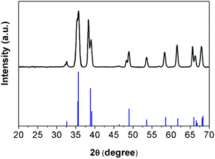 | ||
| Fig. 3 X-ray diffraction patterns of nanowires after oxidation (top) in comparison with standard CuO reference (shown in blue color, bottom). | ||
Sensing properties
The sensing properties of the CuO nanowires towards H2S detection was first examined by running a full test cycle upon H2S exposure of 200 ppb at 180 °C as shown in Fig. 4. Initially, the CuO nanowire sensor gave a stable baseline in the dry air condition. Then, as expected for p-type semiconducting metal oxide materials, a positive sensor response (increased resistance) was measured when H2S gas was introduced into the system at around 25 min. After the H2S input was turned off, the signal gradually recovered back to the original baseline and became stable again at the end time period.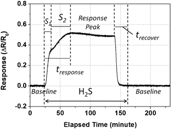 | ||
| Fig. 4 A full test cycle of the CuO nanowire sensor responding to H2S exposure (200 ppb) at a working temperature of 180 °C. | ||
It is worth mentioning that during this process an interesting two-stage response was observed as the frontal curve of the response peak exhibits two distinguished slopes before reaching the plateau region. According to the literature, there are two major types of reactions regarding CuO or CuO-containing metal oxide materials with H2S. One is the oxidation of H2S with adsorbed oxygen species on the CuO surface (eqn (1) and (2)),21–23 which is very similar to the sensing mechanism of most semiconducting metal oxide materials.
| H2S (ads) + 3O− (ads) → H2O + SO2 + 3e | (1) |
| H2S (ads) + 3O2− (ads) → H2O + SO2 + 3e | (2) |
| H2S (ads) + CuO → CuS + H2O | (3) |
These type of reactions will result in the generation of SO2 and H2O, and the return of free electrons from adsorbed oxygen to CuO. These electrons further neutralize with intrinsic holes to decrease the carrier concentration of CuO, hence an increased resistance can be measured. The other type of reaction is simply the generation of CuS (eqn (3)),10,24,25 which is a metallic-like conductor. Its impact on the material will be reduced resistance.
This two-stage dynamic response curve indicates that H2S prefers oxidation over dissociation, because the adsorbed oxygen species are more active than CuO. So it is reasonable to believe that in the first segment S1 (Fig. 4), the H2S oxidation dominates the process exclusively. With continuous H2S input, the consumption of the adsorbed oxygen on the CuO surface was kept at a rapid rate. When its concentration dropped to a certain level, that excessive amount of H2S would react with CuO directly. This triggered the formation of CuS, leading to a counter effect on the resistance change. Because of this compensation, the response curve of the second segment S2 displayed a gentle slope compared to that in S1. These two types of reaction would continue to compete until they reached a steady state, as seen in the flat area at the end of the response peak. Recovery of resistance occurred immediately after the input gas was switched back to dry air only. The same reversible response was previous reported by Chen et al.10 in a vertically aligned CuO nanowire system at 500 ppb and 1 ppm levels without further investigation on response dynamics. Here we significantly lowered the H2S exposure down to ∼10 ppb, and observed this unique two-stage response.
From this complete testing cycle, the response time tS for reaching the maximum ΔR was measured to be 42 min. Similarly, the recovery time tR was measured to be 20 min. Considering the relatively long time taken for the H2S sensing of CuO nanowires to reach the plateau stage, in the following experiments, we sampled the sensor response data upon 10 min exposure of H2S and after a 15 min recovery session, at various concentration levels and operating temperatures.
One key factor in the performance of solid-state gas sensors is the working temperature. To find out its optimum value for this CuO nanowire sensor, sensing tests towards 10 min exposure of 100 ppb H2S were conducted at 25 °C, 80 °C, 140 °C, 180 °C, 240 °C, 280 °C, 320 °C, 380 °C, and 420 °C. The dynamic response curves collected from these 9 temperature points are shown as a layout in Fig. 5a, whereas the results of response versus temperature are plotted in Fig. 5b. Although it has been well accepted that for most metal oxide materials, elevated working temperature above 300 °C is normally preferable, CuO sensors, on the other hand, have been reported to have a medium to low working temperature range of about 160–240 °C.10,26 From the results of our experiments, the highest resistance change appears at 180 °C as a 23.7% increase in resistance. Noticeably, a weak sensor response was observed at 25 °C, which is considered to be room temperature. In the high temperature region (above 300 °C), the CuO nanowire sensor still showed moderate responses to H2S of 12.2% to 16.6% resistance changes. From Fig. 5b, although the trend of how response changes with temperature was not linear or monotonic, it still showed the sensing property has a strong dependency on temperature. Since the optimized temperature for the CuO nanowire sensor is only 180 °C, it will benefit future sensor devices in terms of saving energy and causing less safety issues.
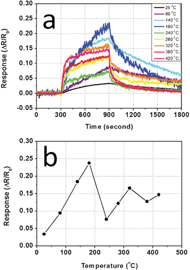 | ||
| Fig. 5 (a) Dynamic response curves of the CuO nanowire sensor responding to 100 ppb H2S at different working temperatures; (b) Sensor response as a function of working temperature. | ||
The temperature influence can also be reflected in response kinetics. Obviously, as the testing temperature rises from 25 °C to 420 °C, the slope of the response curve becomes steeper. Similarly, the recovery process displays the same trend as faster recovery was observed at the higher working temperatures. The reason for this phenomenon could be related to the fact that, both physical adsorption/desorption and chemical reactions on the metal oxide surface are affected by the temperature. Higher temperature leads to accelerated diffusion, ionization and reaction rate, and at a macroscopic level, these add up to cause faster response and recovery. However, in the case of CuO nanowires, the pre-adsorbed oxygen concentration might be higher in the medium to low temperature range, so even though the sensing speed is better, the response is still not as good as that at lower temperatures.
After the working temperature was optimized to be 180 °C, a series of experiments were conducted at this temperature to study the sensor response at various concentration levels, beginning with 10 ppb. The results are shown in Fig. 6, as a layout of the dynamic response curves towards H2S exposure of 10, 20, 50 and 100 ppb. At 10 ppb, H2S exposure resulted in a 4.8% resistance increase, based on which the detection limit (10 min exposure) of this CuO nanowire sensor was estimated to be 2.5 ppb by S/N = 3. This very small value proved that these CuO nanowires could outperform most other metal oxide materials currently available for H2S sensing.10,24,25,26. Besides the high sensitivity, good repeatability was also demonstrated as shown in Fig. 6. At each concentration level, three subsequent exposure–purging cycles were conducted, and only small variations were observed between the three peaks.
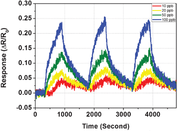 | ||
| Fig. 6 Dynamic response curves of the CuO nanowire sensor upon H2S exposure from 10 to 100 ppb; each concentration measurement was repeated three times. | ||
Furthermore, the tests were expanded as we measured the sensor response up to 1000 ppb, and the results are given in Fig. 7a, as response plotted versus concentration level from 10 to 1000 ppb with errors bar. This figure illustrates the trend of how sensor response increased from a few percent to over one hundred percent with the ascending temperature setting. The trend roughly follows a hyperbolic curve as most commonly seen in chemiresistive sensors—a very fast increase in the low concentration region, followed by a gentle slope in the high concentration region. According to Guidotti's toxicological report in 2010,27 the rise of respiratory illness in children has been associated with H2S exposure levels less than 100 ppb, so the capability of detecting low concentration H2S is critical for evaluating a H2S sensor’s performance. Here, special attention was paid to the linear region at the lower concentration range (10–100 ppb). In Fig. 7b, a fitted line is presented to show the linearity of the points in the lower concentration range. It is colored in red and has a slope of 0.19% per ppb, with a R-square value of 0.99846 indicating a good linearity for future device integration. Another important property in favour of device integration is the reproducibility of the CuO nanowire sensor chips. For chips that have been tested in this experiment, although the absolute resistance may slightly vary due to the variance of the density of the CuO nanowires dispersed on the electrode surfaces, the sensor response data in terms of resistance change in percent, measured under the same conditions, are fairly close.
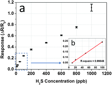 | ||
| Fig. 7 (a) Sensor response versus H2S concentration from 10 to 1000 ppb; (b) a magnified image of the linear region (the red line is a linear fitting of the experimental results). | ||
To further illustrate the outstanding performance of the CuO nanowires over other commonly used sensing materials such as SnO2, a SnO2 nanowire sensor was fabricated following the same procedures. Fig. 8 shows the 10 min 100 ppb H2S exposure response of CuO at 180 °C, and SnO2 nanowires at 180 °C and 420 °C. The H2S response of this particular sensor was first measured at 180 °C, which is the optimized temperature setting for CuO nanowire sensor. No obvious response peak was observed for the SnO2 sensor at 180 °C (green line) in Fig. 8. From our previous study, this is not surprising because SnO2 nanowire sensors tend to have a preferred working temperature at a relatively high temperature range.18 Even at the highest available working temperature of 420 °C, SnO2 nanowires caused only a 15% decrease in resistance. Unlike CuO, SnO2 is a typical n-type semiconducting metal oxide that has oxygen deficiency in its crystal structure. So the return of free electrons generated from the same oxidation reaction of H2S with adsorbed oxygen species, in this case, lead to decreased resistance. By comparing the sensitivity values, it is convincing that CuO has advantages over SnO2 in its lower working temperature and higher response.
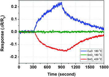 | ||
| Fig. 8 Sensor response of CuO nanowires at 180 °C, and SnO2 nanowires at 180 °C and 420 °C toward 100 ppb H2S exposure of 10 min and 15 min dry air purging. | ||
Conclusions
Pure Cu nanowires were firstly synthesized in large numbers using an electrodeposition method and CuO nanowires were obtained by oxidizing Cu nanowires at 700 °C for over 4 h. For sensor device integration, DEP assembly was used as an efficient way to align nanowires onto a commercial sensor platform. Sensing properties of the CuO nanowire sensor were evaluated in multiple aspects, including response kinetics, temperature dependence and resistance change. The co-existence of two competing reactions between H2S and adsorbed oxygen ions or CuO has resulted in a unique two-stage response upon H2S exposure. The second response section showed a dampened resistance increase compared to the first stage. The sensor performance also heavily depended on the working temperature. Unlike most other metal oxide sensing materials, the CuO nanowire sensor favoured a temperature region around 180 °C, and could respond to H2S in most temperature setting, even at room temperature. Furthermore, at the optimized working temperature, this CuO nanowire sensor had a measurable response to H2S exposure as low as 10 ppb, and the detection limit was calculated to be 2.5 ppb.Acknowledgements
We are thankful for the financial support from the National Science Foundation (award number ECCS-0731125). Partial funding from 3M Company (3M Non-Tenured Faculty Grant) is acknowledged.References
- R. Reiffenstein, W. C. Hulbert and S. H. Roth, Annu. Rev. Pharmacol., 1992, 32, 109–134 CrossRef CAS.
- D. Glass, Ann. Occup. Hyg., 1990, 34, 323–327 CrossRef CAS.
- S. Gautam, A. Venkatanarayanan and B. Parthasarathy, Ann. Occup. Hyg., 1979, 22, 371–382 CrossRef CAS.
- R. C. John, A. D. Pelton, A. L. Young, W. T. Thompson, I. G. Wright and T. M. Besmann, Mater. Res., 2004, 7, 163–173 CrossRef CAS.
- R. Eschenbruch, P. Bonish and B. Fisher, Vitis, 1978, 17, 67–74 CAS.
- M. G. Costigan, Occup. Environ. Med., 2003, 60, 308–312 CrossRef.
- D. B. Richardson, Am. J. Ind. Med., 1995, 28, 99–108 CrossRef CAS.
- H. Liu, S. Gong, Y. Hu, J. Liu and D. Zhou, Sens. Actuators, B, 2009, 140, 190–195 CrossRef.
- V. Kapse, S. Ghosh, G. Chaudhari and F. Raghuwanshi, Talanta, 2008, 76, 610–616 CrossRef CAS.
- J. Chen, K. Wang, L. Hartman and W. Zhou, J. Phys. Chem. C, 2008, 112, 16017–16021 CAS.
- C. S. Rout, M. Hegde and C. Rao, Sens. Actuators, B, 2008, 128, 488–493 CrossRef.
- N. Zhang, K. Yu, Q. Li, Z. Zhu and Q. Wan, J. Appl. Phys., 2008, 103, 104305–104306 CrossRef.
- G. Pollack and D. Trivich, J. Appl. Phys., 1975, 46, 163–172 CrossRef CAS.
- S. Gangwal, J. Stogner, S. Harkins and S. Bossart, Environ. Prog., 1989, 8, 26–34 CrossRef CAS.
- Y. Wang, W. Jia, T. Strout, A. Schempf, H. Zhang, B. Li, J. Cui and Y. Lei, Electroanalysis, 2009, 21, 1432–1438 CrossRef CAS.
- M. J. Song, S. W. Hwang and D. Whang, Talanta, 2010, 80, 1648–1652 CrossRef CAS.
- Z. Liu, T. Yamazaki, Y. Shen, D. Meng, T. Kikuta and N. Nakatani, Chem. Lett., 2008, 37, 296–297 CrossRef CAS.
- X. Li, E. Chin, H. Sun, P. Kurup and Z. Gu, Sens. Actuators, B, 2010, 148, 404–412 CrossRef.
- N. Birks, G. H. Meier and F. S. Pettit, Introduction to the High-temperature Oxidation of Metals, Cambridge University Press, 2006 Search PubMed.
- E. G. Seebauer and M. C. Kratzer, Charged Semiconductor Defects: Structure, Thermodynamics and Diffusion, Springer Verlag, 2008 Search PubMed.
- V. Malyshev and A. Pislyakov, Sens. Actuators, B, 1998, 47, 181–188 CrossRef.
- M. V. Vaishampayan, R. G. Deshmukh, P. Walke and I. Mulla, Mater. Chem. Phys., 2008, 109, 230–234 CrossRef CAS.
- J. Xu, X. Wang and J. Shen, Sens. Actuators, B, 2006, 115, 642–646 CrossRef.
- A. Chowdhuri, V. Gupta and K. Sreenivas, Sens. Actuators, B, 2003, 93, 572–579 CrossRef.
- X. Kong and Y. Li, Sens. Actuators, B, 2005, 105, 449–453 CrossRef.
- F. Zhang, A. Zhu, Y. Luo, Y. Tian, J. Yang and Y. Qin, J. Phys. Chem. C, 2010, 114, 19214–19219 CAS.
- T. Guidotti, Int. J. Toxicol., 2010, 29, 569–581 CrossRef CAS.
| This journal is © The Royal Society of Chemistry 2012 |