Growth selectivity of hexagonal-boron nitride layers on Ni with various crystal orientations†
Yi-Hsien
Lee
*a,
Keng-Ku
Liu
a,
Ang-Yu
Lu
a,
Chih-Yu
Wu
a,
Cheng-Te
Lin
a,
Wenjing
Zhang
a,
Ching-Yuan
Su
a,
Chang-Lung
Hsu
ab,
Tsung-Wu
Lin
c,
Kung-Hwu
Wei
b,
Yumeng
Shi
d and
Lain-Jong
Li
*ae
aResearch Center for Applied Sciences, Academia Sinica, Taipei, 11529, Taiwan. E-mail: yhlee@phys.sinica.edu.tw and (L. J. Li): lanceli@gate.sinica.edu.tw
bDepartment of Material Science and Engineering, National Chiao Tung University, Hsinchu 300, Taiwan
cDepartment of Chemistry, Tunghai University, No. 181, Sec. 3,Taichung Port Rd., Taichung City, 40704, Taiwan
dDepartment of Electrical Engineering and Computer Sciences, Massachusetts Institute of Technology Cambridge, Massachusetts 02139, USA
eDepartment of Photonics, National Chiao Tung University, HsinChu 300, Taiwan.
First published on 1st November 2011
Abstract
Layered hexagonal-boron nitride (h-BN) films were synthesized by chemical vapor deposition (CVD) on Ni foils using ammonia borane as a precursor. Confocal Raman spectroscopy and electron backscatter diffraction (EBSD) were used to probe the effect of underlying Ni crystals with various orientations on growth behaviors of h-BN layers. The growth of the h-BN layers strongly depends on the Ni crystal orientations, where the growth rate of h-BN is larger on Ni(100)-like crystal surfaces but the growth on Ni(111)-like surfaces is not detectable, suggesting that Ni (100)-like facets are likely to promote the growth of h-BN compared with Ni (111)-like surfaces. The observation is in clear contrast to the reported growth of h-BN on Ni(111) in an ultrahigh vacuum environment. The as-grown CVD h-BN films on Ni exhibit a layered structure as revealed by atomic force microscopy (AFM). Thin h-BN layers are found on the Ni domain with a low growth rate. The observation of h-BN growth on various Ni grains may provide insights for the control of thickness, size and morphology of CVD h-BN films.
Two-dimensional and covalently bonded materials, such as graphene, have recently attracted considerable attentions due to its high chemical stability, excellent electrical performance as a conductor1,2 and potential for ultra-thin electronic devices.3–6Graphene-based devices have been fabricated on many different supporting substrates. It has been revealed that the carrier mobility of graphene is markedly reduced by the charge impurities, substrate dangling bonds, surface roughness and other disorders induced by the substrates.4,5,7–9 Structurally suspended graphene exhibits high electrical performance due to the removal of substrate-induced defects but it is of great challenge to integrate it with the existing fabrication techniques. Recently, mechanically exfoliated hexagonal-boron nitride (h-BN) layers have been used as the substrates for hosting graphene layers, where the graphene exhibits nearly intrinsic high carrier mobility due to the fact that h-BN is topographically smooth, trap-charge and defect free.5,6,9 Moreover, h-BN could break the in-plane symmetry of graphene, inducing an energy gap in graphene.10,11
Few-layer h-BN has been obtained by mechanical exfoliation,5,6 chemical exfoliation,12 extended sonication in solution13 and surface segregation of catalyst alloy.14 However, the limited flake size of the h-BN films produced by these methods hinders their applications in large area devices. Chemical vapor deposition (CVD) is promising for synthesizing large area and high quality graphene and graphene-like two dimensional materials.15–18 Recently, h-BN thin films have been successfully prepared by CVD using various precursors and catalytic metals. Shi et al. obtained h-BN thin layers on Ni thin films using borazine as the precursor,17 while Song et al. demonstrated the synthesis of h-BN on Cu foils using the ammonia borane precursor.18 To our knowledge, most studies on h-BN are focused on the exfoliated h-BN flakes because the fabrication by mechanical exfoliation is simple. Only a few studies have reported the synthesis of h-BN layer with CVD. The fundamental growth mechanism still remains unclear. Understanding the layer growth behaviors of the h-BN is essential for future electronic applications and bandgap opening of monolayer graphene. In this contribution, the polycrystalline Ni foil was firstly adopted as the substrate for synthesizing CVD h-BN layers. We study the growth of h-BN layer on Ni foils using ammonia borane as a precursor in a diluted hydrogen atmosphere. Confocal Raman spectroscopy and electron backscatter diffraction (EBSD) were used to study the effects of underlying Ni crystal orientations on the growth behavior of the h-BN layers. The growth of the h-BN layers strongly depends on the underlying Ni crystal orientations. We observe that the growth rate is larger on Ni(100)-like crystal surfaces but the growth on Ni(111)-like surfaces is too slow to be detected.
The h-BN films were synthesized in a quartz tube reaction chamber placed in a furnace using polycrystalline Ni foils (99%, Nilaco) as catalytic substrates. Ni foil was first loaded into the CVD chamber and annealed at 800 °C for 50 min with Ar/H2 (Ar = 350 sccm and H2 = 70 sccm; at 500 Torr) to remove the native oxide. Ammonia borane (NH3–BH3; 96%, Alfa Aesar) was sublimated at 120–125 °C in a vessel connected to the reaction chamber and carried into the reaction chamber by an Ar flow (3 sccm). The carrying gas was kept flowing for 80 min, while the growth chamber was kept at 10 Torr (H2: 50 sccm, Ar: 300 sccm) at 800 °C. Fig. 1a and 1b show the optical images of the as-synthesized h-BN films on Ni foils and those transferred onto 300 nm SiO2/Si substrate. In general, the darker areas in Fig. 1a indicate the presence of the thick h-BN films and the shape of the h-BN films follows the shape of underlying Ni grains. After transferring all the as-grown h-BN films on top of the Ni foils to a 300 nm SiO2/Si substrate, thinner h-BN layers can then be clearly visualized under an optical microscope (Fig. 1b). Note that the h-BN films were transferred onto a SiO2 substrate following the similar processes reported for graphene transfer,19 where a layer of poly(methyl methacrylate) (PMMA) was coated on h-BN/Ni followed by dipping in a diluted hydrochloride (HCl) solution to etch the interfacial Ni and to peel off the PMMA-covered h-BN films. The PMMA-covered h-BN films were then put onto SiO2/Si substrates followed by PMMA removal using acetone. Similar to the case of graphene on 300 nm SiO2/Si substrates observed in optical microscopy, the film with a larger color contrast is with a larger film thickness. The thickness for several selected h-BN flakes measured by AFM are directly labeled in Fig. 1b. The domain area of the as-synthesized h-BN films observed in an optical microscope, regardless of its color contrast, is comparable to the grain size of the polycrystalline Ni foils. Moreover, a few h-BN domains exhibit sharp facets with structural twins that are commonly observed in the Ni foils.20 These results suggest that the growth of h-BN films is strongly affected by the structure of the underlying Ni crystals.
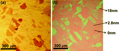 | ||
| Fig. 1 Optical micrographs for (a) as-synthesized h-BN films on Ni foils and (b) h-BN films transferred onto 300 nm SiO2/Si substrates. | ||
Chemical structures are characterized by X-ray photoelectron spectroscopy (XPS; VG Scientific Microlab 350). XPS measurements were performed with an Mg-Kα X-ray source on the samples. Fig. 2 shows the XPS spectrum for the transferred sample on SiO2/Si, where two peaks at 190.3 eV and 398.2 eV are identified as the binding energies of the B 1s and N 1s electrons respectively. These energy values suggest that the B and N in our samples are trivalent-bonded.21 The spot size in our XPS analysis is about three millimetres; thus, the XPS result involves contributions from all the thick and thin h-BN layers. The stoichiometric ratio of the films, estimated from the integrated XPS peak intensity of B 1s and N 1s, is about 1![[thin space (1/6-em)]](https://www.rsc.org/images/entities/char_2009.gif) :1.01, corroborating that these films are h-BN. Electron backscatter diffraction (EBSD; HKL, Oxford Instruments) is used to locally probe the lattice information of the Ni crystals underneath the h-BN films. All the EBSD information was obtained from the analysis of Kikuchi diffraction pattern.22 Typically the probing depth of the EBSD is around 50–100 nm from the surface. The spatial resolution of our EBSD system is ∼100 nm. Fig. 3a and 3b show the optical microscopy and SEM images for a selected area of the h-BN on a Ni foil. The dotted black rectangle indicates the area with EBSD mapping analysis, where the surface of the Ni substrates can be classified into three major crystal orientations Ni(100), Ni(101) and Ni(111) shown as red, green and blue colors in the Miller index map (right figure in 3c). Fig. 3c (left) displays the orientations identified from the Ni grains in the selected area, where we can see Ni(106), Ni(156), and Ni(536) grains which are Ni(100)-, Ni(101)- and Ni(111)-like in crystal orientations respectively. Surface morphology was obtained with commercial AFM (Veeco Dimension-Icon). Fig. 3d shows the surface morphology of the square area that three grains Ni(106), Ni(156) and Ni(536) meet, as indicated by thick red lines in Fig. 3b. The topography of the Ni(536) surfaces are quite different from the others because of the absence of h-BN films on them. Some flat and thick h-BN films can be seen on the Ni(106) grain and flat films with a typical wrinkle structure are observed on top of Ni(156). To characterize the growth dependence of h-BN films on various Ni grains, confocal Raman spectroscopy (excitation laser 473 nm; spot size ∼0.5 μm; NT-MDT) was adopted to monitor the h-BN characteristic peak at ∼1368 cm−1.6,17,18 As shown in Fig. 3e, the strongest Raman intensity of the peak is obtained for the h-BN domain grown on Ni(106). The intensity of the film on Ni(156) is significantly lower than that on Ni(106). The presence of the Raman peak at 1368 cm−1 for our h-BN films corroborates the success in synthesizing h-BN layers on Ni substrates. Surprisingly, the Raman peak for the h-BN film is not detectable on Ni(536) grains. These observations suggest that the crystal orientations of the underlying Ni grains strongly affect the growth rate of the h-BN films. Figure S1 provides more EBSD and SEM images, which also lead to the same conclusion that the growth of h-BN is appreciable on Ni(100)-like but it is not detectable on Ni(111)-like crystals.†
:1.01, corroborating that these films are h-BN. Electron backscatter diffraction (EBSD; HKL, Oxford Instruments) is used to locally probe the lattice information of the Ni crystals underneath the h-BN films. All the EBSD information was obtained from the analysis of Kikuchi diffraction pattern.22 Typically the probing depth of the EBSD is around 50–100 nm from the surface. The spatial resolution of our EBSD system is ∼100 nm. Fig. 3a and 3b show the optical microscopy and SEM images for a selected area of the h-BN on a Ni foil. The dotted black rectangle indicates the area with EBSD mapping analysis, where the surface of the Ni substrates can be classified into three major crystal orientations Ni(100), Ni(101) and Ni(111) shown as red, green and blue colors in the Miller index map (right figure in 3c). Fig. 3c (left) displays the orientations identified from the Ni grains in the selected area, where we can see Ni(106), Ni(156), and Ni(536) grains which are Ni(100)-, Ni(101)- and Ni(111)-like in crystal orientations respectively. Surface morphology was obtained with commercial AFM (Veeco Dimension-Icon). Fig. 3d shows the surface morphology of the square area that three grains Ni(106), Ni(156) and Ni(536) meet, as indicated by thick red lines in Fig. 3b. The topography of the Ni(536) surfaces are quite different from the others because of the absence of h-BN films on them. Some flat and thick h-BN films can be seen on the Ni(106) grain and flat films with a typical wrinkle structure are observed on top of Ni(156). To characterize the growth dependence of h-BN films on various Ni grains, confocal Raman spectroscopy (excitation laser 473 nm; spot size ∼0.5 μm; NT-MDT) was adopted to monitor the h-BN characteristic peak at ∼1368 cm−1.6,17,18 As shown in Fig. 3e, the strongest Raman intensity of the peak is obtained for the h-BN domain grown on Ni(106). The intensity of the film on Ni(156) is significantly lower than that on Ni(106). The presence of the Raman peak at 1368 cm−1 for our h-BN films corroborates the success in synthesizing h-BN layers on Ni substrates. Surprisingly, the Raman peak for the h-BN film is not detectable on Ni(536) grains. These observations suggest that the crystal orientations of the underlying Ni grains strongly affect the growth rate of the h-BN films. Figure S1 provides more EBSD and SEM images, which also lead to the same conclusion that the growth of h-BN is appreciable on Ni(100)-like but it is not detectable on Ni(111)-like crystals.†
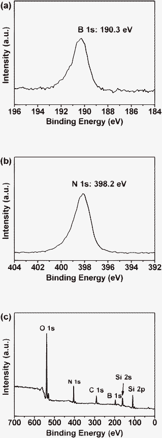 | ||
| Fig. 2 XPS results for the h-BN film. (a) B 1 s (at 190.3 eV), (b) N 1 s (at 398.2 eV), (c) survey spectrum. | ||
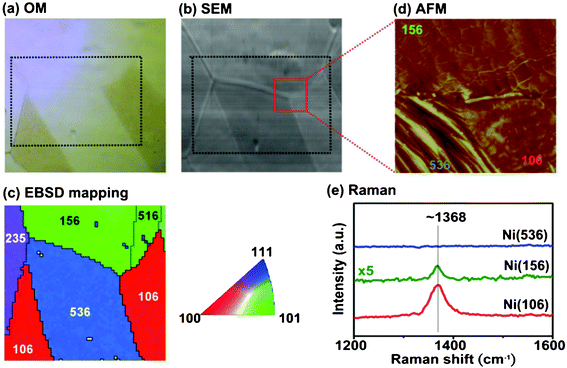 | ||
| Fig. 3 (a) OM and (b) SEM images of the h-BN films that are grown on Ni foils. (c) EBSD image of the marked area with white dashed line. (d) AFM image for the marked area in (b). (e) Raman spectra of the h-BN films on Ni foil with various orientations. | ||
To reveal the morphology of the h-BN grown on different Ni grains, we examine the topography of two distinct h-BN domains grown with high and low growth rates respectively labeled as I and II in the optical micrograph (Fig. 4a). The AFM image in Fig. 4c demonstrates that the h-BN on the grain I exhibits a flat and thick layered structure (∼12 nm). In contrast, Fig. 4b shows that the h-BN layers on the low growth rate grain II are thinner but discontinuous. The magnified AFM image for the marked area reveals that these h-BN thin flakes are irregular in shape, where the cross-section profiles of two selected small thin flakes are shown in Fig. 4d and the thickness is 1.0 and 1.6 nm respectively. Based on the thickness, these h-BN flakes are likely to be a mono- and bi-layer. Note that an apparent thickness less than 1.2 nm could be considered as a monolayer as reported.23,24 Qualitative examination of the h-BN films with various thicknesses was also carried out by Raman measurements. Fig. 5a shows the optical micrograph of the area selected for Raman mapping studies. Fig. 5b and 5c respectively show the mapping constructed by plotting the integrated h-BN peak (at 1368 cm−1) intensity and the peak width in confocal Raman measurements, with a typical optical resolution of ca. 0.5 mm. The peak intensity clearly increases with the thickness of the h-BN domain, consistent with the observation with the exfoliated h-BN layers.6 Interestingly, the peak width does not significantly vary with the h-BN thickness, implying that the crystalline quality of the h-BN films with various thicknesses is quite comparable.
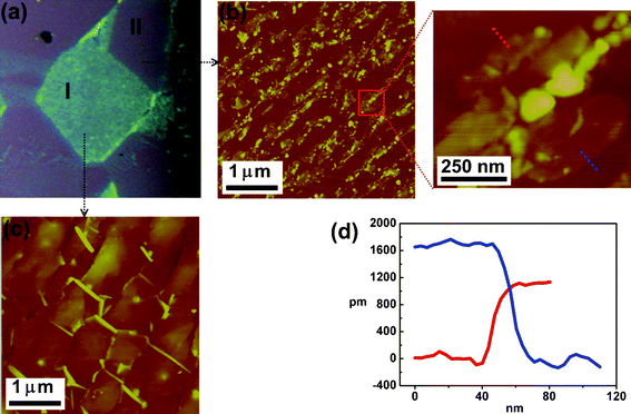 | ||
| Fig. 4 (a) OM images of the h-BN films that are transferred onto SiO2 substrates. Typical AFM images of h-BN films on (b) part II (c) part I regions. Enlarged AFM image in (b) shows the h-BN flakes. (d) Line profiles of the h-BN flakes in different areas. | ||
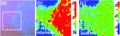 | ||
| Fig. 5 (a) OM images of the h-BN films that are transferred onto SiO2/Si substrate. Raman mapping is obtained over the marked area for the h-BN peak at 1368 cm−1: (b) peak intensity and (c) peak width. | ||
It is noteworthy to point out that the h-BN growth on Ni(111) in an ultrahigh vacuum environment has been reported and it is generally explained by a thermodynamic factor that there is a small lattice mismatch of about 0.5% between Ni(111) and h-BN.25–29 However, diversities in the CVD growth mechanisms are usually found due to the possibility of having few intermediate reaction states and the complicated mutual influences between precursor species and metal surafces.30–36 Our experimental results show that in the CVD growth condition using ammonia borane as a precursor with the presence of hydrogen gas, the growth of h-BN on Ni(100)-like orientation is not prohibited. In contrast, the growth on Ni(111)-like surface is not preferred. Some early studies have also discussed that the co-adsorbed ammonia and borane on Ni(100) are able to react to form a layer of h-BN film by thermal heating, although the h-BN on Ni(100) is not the most thermodynamically preferable structure.37,38 Moreover, based on the theoretical prediction for the adsorption and aggregation processes of the adatom on catalytic metal surfaces, the growth of honeycomb-based materials is expected to be strongly dependent on the surface energy and surface structure of the substrates.31,39 The energy for the entire adsorption and aggregation process may substantially vary with reaction path and active reaction species on the surfaces. We believe that one of the crucial factors that we need to consider is the high surface energy of Ni(100)-like surfaces.40 The ammonia borane may quickly adhere to the Ni(100) surface to reduce its energy, which leads to the fast nucleation and growth of the h-BN layer. It is also possible that the Ni surfaces with various crystal orientations exhibit different catalytic reaction activities,39 which may result in the different h-BN growth rates as observed in our experiments. Further works are necessary to obtain a definite mechanism for the fundamental processes. The observation of high growth rate on Ni(100) implies that kinetic rather than thermodynamic control for the CVD growth of h-BN on Ni should be taken into consideration.
In summary, layered h-BN films were synthesized on Ni foils with CVD methods, evidenced by the observation of Raman peak at 1368 cm−1 and the B 1s and N 1s binding energies at 190.3 eV and 398.2 eV respectively. Growth of the h-BN films exhibits obvious Ni-grain dependency, where the growth rate of h-BN is larger on Ni(100)- or Ni(100)-like crystal surfaces but the growth on Ni(111)- or Ni(111)-like surfaces is non-detectable, indicating that kinetic rather than thermodynamic control for the CVD growth of h-BN on Ni should be taken into consideration.
Acknowledgements
This research was supported by Academia Sinica (Nano Program) and National Science Council Taiwan (NSC-99-2112-M-001-021-MY3, 99-2738-M-001-001 and Nano program). We also acknowledge the support from 5y5b project of National Tsing Hua University, Taiwan.References
- A. K. Geim and K. S. Novoselov, Nat. Mater., 2007, 6, 183–191 CrossRef CAS
.
- A. H. Neto Castro, F. Guinea, N. M. R. Peres, K. S. Novoselov and A. K. Geim, Rev. Mod. Phys., 2009, 81, 109–162 CrossRef
- M. Corso, W. Auwarter, M. Muntwiler, T. Anna, T. Greber and J. Osterwalder, Science, 2004, 303, 217–220 CrossRef CAS
- K. Nomura and A. H. MacDonald, Phys. Rev. Lett., 2007, 98, 076602 CrossRef
- C. R. Dean, A. F. Young, P. Cadden-Zimansky, L. Wang, H. Ren, K. Watanabe, T. Taniguchi, P. Kim, J. Hone and K. L. Shepard, Nat. Nanotechnol., 2010, 5, 722–726 CrossRef CAS
- R. V. Gorbachev, I. Riaz, R. R. Nair, R. Jalil, L. Britnell, B. D. Belle, E. W. Hill, K. S. Novoselov, K. Watanabe, T. Taniguchi, A. K. Geim and P. Blake, Small, 2011, 7, 465–468 CrossRef CAS
- J. H. Chen, C. Jang, S. Xiao, M. Ishigami and M. S. Fuhrer, Nat. Nanotechnol., 2008, 3, 206–209 CrossRef CAS
- T. Ando, J. Phys. Soc. Jpn., 2006, 75, 074716 CrossRef
- R. Decker, Y. Wang, V. W. Brar, W. Regan, H. Z. Tsai, Q. Wu, W. Gannett, A. Zettl and M. F. Crommie, Nano Lett., 2011, 11, 2291–2295 CrossRef CAS
- G. Giovannetti, P. A. Khomyakov, G. Brocks, P. J. Kelly and J. van den Brink, Phys. Rev. B: Condens. Matter Mater. Phys., 2007, 76, 073103 CrossRef
- K. S. Novoselov, Nat. Mater., 2007, 6, 720–721 CrossRef CAS
- Y. Wang, Z. Shi and J. Yin, J. Mater. Chem., 2011, 21, 11371 RSC
- C. Zhi, Y. Bando, C. Tang, H. Kuwahara and D. Golberg, Adv. Mater., 2009, 21, 2889–2893 CrossRef CAS
- M. Xu, D. Fujita, H. Chen and N. Hanagata, Nanoscale, 2011, 3, 2854 RSC
- A. N. Obraztsov, Nat. Nanotechnol., 2009, 4, 212–213 CrossRef CAS
- X. S. Li, W. W. Cai, J. H. An, S. Kim, J. Nah, D. X. Yang, R. Piner, A. Velamakanni, I. Jung, E. Tutuc, S. K. Banerjee, L. Colombo and R. S. Ruoff, Science, 2009, 324, 1312–1314 CrossRef CAS
- Y. Shi, C. Hamsen, X. Jia, K. K. Kim, A. Reina, M. Hofmann, A. L. Hsu, K. Zhang, H. Li, Z. Y. Juang, M. S. Dresselhaus, L. J. Li and J. Kong, Nano Lett., 2010, 10, 4134–4139 CrossRef CAS
- L. Song, L. Ci, H. Lu, P. B. Sorokin, C. Jin, J. Ni, A. G. Kvashnin, D. G. Kvashnin, J. Lou, B. I. Yakobson and P. M. Ajayan, Nano Lett., 2010, 10, 3209–3215 CrossRef CAS
- C. Y. Su, D. Fu, A. Y. Lu, K. K. Liu, Y. Xu, Z. Y. Juang and L. J. Li, Nanotechnology, 2011, 22, 185309 CrossRef
- L. Murr, Thin Solid Films, 1969, 4, 389–412 CrossRef CAS
-
J. F. Moulder, W. F. Stickle, P. E. Sobol and K. D. Bomben, PHI Handbook of Photoelectron Spectroscopy, Perkin-Elmer Corp. Physical Electronics Division, 1992 Search PubMed
- E. Levine, W. L. Bell and G. Thomas, J. Appl. Phys., 1966, 37, 2141 CrossRef CAS
- A. Gupta, G. Chen, P. Joshi, S. Tadigadapa and P. C. Eklund, Nano Lett., 2006, 6, 2667–2673 CrossRef CAS
- X. Li, X. Wang, L. Zhang, S. Lee and H. Dai, Science, 2008, 319, 1229–1232 CrossRef CAS
- A. Nagashima, N. Tejima, Y. Gamou, T. Kawai and C. Oshima, Phys. Rev. Lett., 1995, 75, 3918–3921 CrossRef CAS
- E. Rokuta, Y. Hasegawa, K. Suzuki, Y. Gamou, C. Oshima and A. Nagashima, Phys. Rev. Lett., 1997, 79, 4609–4612 CrossRef CAS
- W. Auwarter, T. J. Kreutz, T. Greber and J. Osterwalder, Surf. Sci., 1999, 429, 229–236 CrossRef CAS
- G. B. Grad, P. Blaha, K. Schwarz, W. Auwarter and T. Greber, Phys. Rev. B: Condens. Matter, 2003, 68, 085404 CrossRef
- W. Auwarter, H. U. Suter, H. Sachdev and T. Greber, Chem. Mater., 2004, 16, 343–345 CrossRef
- M. Treier, C. A. Pignedoli, T. Laino, R. Rieger, K. Müllen, D. Passerone and R. Fasel, Nat. Chem., 2010, 3, 61–67 CrossRef
- H. Chen, W. Zhu and Z. Zhang, Phys. Rev. Lett., 2010, 104, 186101 CrossRef
- X. S. Li, W. W. Cai, L. Colombo and R. S. Ruoff, Nano Lett., 2009, 9, 4268–4272 CrossRef CAS
- P. Wu, W. Zhang, Z. Li, J. Yang and J. G. Hou, J. Chem. Phys., 2010, 133, 071101 CrossRef
- L. Gao, W. C. Ren, J. P. Zhao, L. P. Ma, Z. Chen and H. M. Cheng, Appl. Phys. Lett., 2010, 97, 183109 CrossRef
- X. S. Li, C. W. Magnuson, A. Venugopal, J. An, J. W. Suk, B. Han, M. Borysiak, W. W. Cai, A. Velamakanni, Y. W. Zhu, L. F. Fu, E. M. Vogel, E. Voelkl, L. Colombo and R. S. Ruoff, Nano Lett., 2010, 10, 4328–4334 CrossRef CAS
- S. Bhaviripudi, X. T. Jia, M. S. Dresselhaus and J. Kong, Nano Lett., 2010, 10, 4128–4133 CrossRef CAS
- T. Greber, L. Brandenberger, M. Corso, A. Tamai and J. Osterwalder, e-J. Surf. Sci. Nanotechnol., 2006, 4, 410 CrossRef CAS
- M. Ryan, A. Desrosiers, W. David, A. Greve, J. Andrew and B. Gellman, Surf. Sci., 1997, 382, 35–48 CrossRef
- R. T. Vang, K. Honkala, S. Dahl, E. K. Vestergaard, J. Schnadt, E. Laegsgaard, B. S. Clausen, J. K. Norskov and F. Besenbacher, Nat. Mater., 2005, 4, 160–162 CrossRef CAS
- T. P. Beebe Jr., D. W. Goodman, B. D. Kay and J. T. Yates Jr., J. Chem. Phys., 1987, 87, 2305–2315 CrossRef
Footnote |
| † Electronic supplementary information (ESI) available: EBSD analysis and AFM results for the h-BN growth are available. See DOI: 10.1039/c1ra00703c |
| This journal is © The Royal Society of Chemistry 2012 |