Graphene synthesis: relationship to applications
Rebecca S.
Edwards
and
Karl S.
Coleman
*
Department of Chemistry, Durham University, South Road, Durham DH1 3LE, UK. E-mail: k.s.coleman@durham.ac.uk
First published on 30th October 2012
Abstract
Graphene is a true wonder material that promises much in a variety of applications that include electronic devices, supercapacitors, batteries, composites, flexible transparent displays and sensors. This review highlights the different methods available for the synthesis of graphene and discusses the viability and practicalities of using the materials produced via these methods for different graphene-based applications.
 Rebecca S. Edwards | Rebecca Edwards received her MChem from Durham University in 2010. She is currently studying for a Ph.D. in chemistry, researching the synthesis and chemistry of graphene, in the nanocarbon group at Durham University led by Karl Coleman. |
 Karl S. Coleman | Karl Coleman is Professor of Chemistry and Nanomaterials in the Department of Chemistry at Durham University. He has extensive experience in the chemical functionalization and characterization of carbon nanotubes. He also works on the synthesis and chemistry of graphene and was named the Royal Society of Chemistry Entrepreneur of the Year in 2011 for his development of new intellectual property for the production of graphene and its commercial exploitation. He is the cofounder of the Chemical Nanosciences and Nanotechnology subject group of the Royal Society of Chemistry. |
1 Introduction
Graphene has been the subject of a wealth of scientific research and received much media attention since the early papers of Geim and Novoselov in 2004,1 for which they later shared the Nobel Prize in Physics in 2010. The catalyst for such interest was the measurement of graphene's exceptional physical properties, including immense strength and extremely high thermal and electrical conductivity. The excellent electrical conductivity, along with the transparency and flexibility of the sheets, has inspired many of the envisaged future applications of graphene such as roll-up and wearable electronics, in addition to the plethora of other real-world applications where graphene may find a use, such as energy storage materials, polymer composites, and transparent electrodes. In this review the different methods of graphene synthesis will be summarised alongside a discussion on the viability and practicalities of using the materials produced via these methods for different graphene-based applications.1.1 Structure
The term ‘graphene’ refers to a single layer of graphite, with sp2 hybridised carbon atoms arranged in an hexagonal lattice and partially filled π-orbitals above and below the plane of the sheet. Seemingly contrary to this, the term ‘graphene’ is commonly prefixed by ‘monolayer’, ‘bilayer’ or ‘few-layer’. This categorisation has been made as the electronic properties of bi and few-layer graphene (where ‘few’ is not rigorously defined but is generally excepted to be <10 layers) are distinct from the electronic properties of graphite.2,3 While monolayer graphene is generally accepted to exists in a rippled form with no stacking of sheets,4–6 few-layer graphene can have a number of stacking arrangements, including ABAB (Bernal stacking), ABCABC (rhombohedral stacking), and less commonly AAA.7,8 Few-layer graphene with no discernible stacking order is also common, and is termed ‘turbostratic’. The interlayer spacing for turbostratic graphene (>0.342 nm) has been found to be larger than that of crystalline graphene (0.335 nm),9 which is thought to enable rotation and translation of the graphene sheets due to the increased distance resulting in weaker inter-planar bonding.The edges of graphene can be described as having armchair or zigzag motifs (Fig. 1), with the two edge types leading to different electronic and magnetic properties.10–12 For the majority of graphene synthesised the edges consist of a mixture of the two motifs, although synthesis of graphene structures with defined edges is a growing area of research given the potential to tune the properties for specific applications.13 In particular graphene nanoribbons; thin strips of graphene, have received a great deal of attention, as reviewed in detail by Dutta and Pati.14
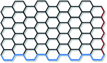 | ||
| Fig. 1 Armchair (blue) and zigzag (red) edges in monolayer graphene. | ||
1.2 Properties
It is easy to see why graphene has been termed a “wonder material” when looking at the physical properties measured and predicted. As a single layer of carbon atoms, graphene is the thinnest material known yet it is impermeable to gases,15 and it is stronger than steel (Young's modulus ∼ 1 TPa).16 Furthermore graphene's room temperature thermal conductivity (up to ∼5000 W m−1 K−1) rivals the values obtained for bundles of carbon nanotubes and is over double the next best thermal conductor known, diamond.17 Being single layer, graphene also has an extremely high surface area with a theoretical value of 2630 m2 g−1 and is almost transparent, absorbing only ∼2.3% of white light.18 Graphene has also shown good ‘foldability’, recovering it's electrical properties after bending and unbending.19 The properties of graphene have been reviewed in detail elsewhere.20,21The electronic properties have perhaps received the most attention. Graphene has been shown to have extremely high charge carrier mobilities, with values in excess of 200![[thin space (1/6-em)]](https://www.rsc.org/images/entities/char_2009.gif) 000 cm2 V−1 s−1 reported for freely suspended graphene,22 making it an excellent conductor of electricity. This conductivity arises due to the unusual behaviour of the propagating electrons in graphene, which are said to act as massless fermions; best described by a Dirac-like equation rather than the Schrödinger equation used for conventional systems.20 As a consequence of this, electrons in graphene reportedly travel at a Fermi velocity (vF) of ∼1 × 10⁶ m s−1, and can travel distances in the order of micrometers without scattering; a phenomenon which is referred to as ballistic transport.23 This behaviour, and a number of other quantum relativistic effects exhibited by graphene such as the quantum Hall effect,24 makes graphene an interesting material to study from a fundamental physics perspective.25
000 cm2 V−1 s−1 reported for freely suspended graphene,22 making it an excellent conductor of electricity. This conductivity arises due to the unusual behaviour of the propagating electrons in graphene, which are said to act as massless fermions; best described by a Dirac-like equation rather than the Schrödinger equation used for conventional systems.20 As a consequence of this, electrons in graphene reportedly travel at a Fermi velocity (vF) of ∼1 × 10⁶ m s−1, and can travel distances in the order of micrometers without scattering; a phenomenon which is referred to as ballistic transport.23 This behaviour, and a number of other quantum relativistic effects exhibited by graphene such as the quantum Hall effect,24 makes graphene an interesting material to study from a fundamental physics perspective.25
It should be noted that the amazing properties have been recorded on high quality, small area monolayer graphene samples, and may not be achievable for larger, bulk scale sheets. An example of this is that while ballistic transport is believed to have been observed experimentally by Miao et al. for short graphene strips, evidence of diffusive transport (where scattering does occur) was seen for larger samples.26 Electron scattering of graphene is thought to be caused by impurity defects and topological lattice defects within the graphene sheet,27–29 and to be exasperated further by interactions with the substrates, due to interfacial phonons, surface charge traps and fabrication residues.22
In addition to the surface area of graphene decreasing and its transparency increasing going from monolayer to few-layer graphene,30 the physical properties have also been observed to change upon increasing thickness; although there has only been limited work in this area. The extent to which graphene thickness impacts the properties is likely to vary depending on what's being studied, for example while a gradual change in electronic properties has been calculated for increasing numbers of layers,3,31,32 the experimentally measured thermal conductivity has been shown to be very sensitive to graphene thickness, with the value for four graphene layers being almost the same as that for bulk graphite.33 The change in hardness and elastic modulus have also been reported for different thicknesses of graphene, where a linear decrease for both properties was measured as the number of layers increased up to four.34
2 The relationship between synthesis and applications
A wide range of potential applications for graphene have been proposed based on the multitude of outstanding properties discussed above. The important properties for particular applications are summarised in Table 1. The quantity and form of graphene required varies according to the application; while some applications such as transparent electrodes and sensors require thin films of graphene, other applications such as energy storage devices (such as batteries and supercapacitors) and polymer composites require relatively large quantities of graphene nanosheets or platelets. Furthermore the importance of using high quality graphene will vary with application type, for example no noticeable improvement in electrochemical activity has been observed going from few-layer to monolayer graphene,35 and defects in the material are thought to enhance both electrochemical36 and hydrogen storage37 ability of graphene sheets. The progress in the use of graphene in transistors,38 energy storage devices,39,40 electrodes,41,42 conductive inks,43 polymer composites44 and sensors45 has been reviewed or discussed in detail elsewhere.| Electrical conductivity | Strength | Elasticity | Surface area | Transparency | Thermal conductivity | Chemical inertness | Gas impermeability | |
|---|---|---|---|---|---|---|---|---|
| Transistors | ✓ | ✗ | ✗ | ✗ | ✗ | ✗ | ✓ | ✗ |
| Energy storage devices | ✓ | ✗ | ✗ | ✓ | ✗ | ✗ | ✓ | ✗ |
| Electrodes | ✓ | □ | □ | □ | □ | ✗ | ✓ | ✗ |
| Electrically conductive inks | ✓ | ✗ | ✓ | ✗ | □ | ✗ | ✓ | ✗ |
| Polymer composites | ✓ | ✓ | ✓ | ✓ | □ | ✓ | ✓ | □ |
| Sensors | ✓ | ✗ | □ | ✗ | ✗ | ✗ | ✓ | □ |
In order for graphene's potential to be fully realised, methods for its synthesis need to be developed that can produce good quality material reproducibly. Although this still remains a significant challenge, a number of different routes to synthesise graphene have been demonstrated over recent years, as discussed in Section 3. Some of the methods, by their very nature, lend themselves better to certain applications than others. An example of this is that growth on SiC results in graphene on a wide-band gap semiconductor, which is appropriate for the fabrication of graphene devices operable at room temperature without the need for film transfer,46–48 whereas graphene grown on metals requires transferring to insulating substrates for these applications. In contrast material used for field emission applications needs good ohmic contact so graphene grown on metals is a more obvious choice.49 Similarly graphene films can be formed from individual graphene nanosheets by processes such as spin coating,50 drop casting,51 spraying,52 electrophoretic deposition53 and Langmuir–Blodgett methodologies.54 However, these films are less conducting than large-area graphene films grown on SiC or transition metals due to poor contact between the sheets and defects at the sheet edges, so would be less suitable for applications that require high electrical conductivity.55
In electronics, graphene has the potential to produce smaller, faster devices than silicon but it suffers from the major pitfall that a band gap needs to be engineered to achieve the “on” and “off” states required in digital electronics.56 Graphene can be described as a ‘gapless’ or ‘zero-band-gap’ semiconductor as the conductance and valence bands touch in the Brillouin zone.57 However it is possible to create a band-gap confining the lateral dimension of graphene (for example forming ‘nanoribbons’ by lithography58 or unzipping carbon nanotubes59), applying strain,60 or via electrical or chemical doping.61–63
In displays, graphene has considerable potential to replace indium tin oxide (ITO). Replacing ITO, used as a transparent conducting film in devices such as displays, organic light emitting diodes (OLEDs) and solar cells is a pressing requirement as indium is a finite resource and its cost is rising due to increased use in a range of technological applications.64 A single layer of graphene is more optically transparent than ITO (approx. 98 and 90% respectively) however for the films measured to date it has a much higher electrical resistance (2000–5000 Ω and 50 Ω respectively). This resistance can be reduced by increasing the number of graphene layers but this is achieved at the expense of reduced transparency.65 Alternatively doping with nitric acid has been shown to decrease the sheet resistance of graphene films,66 with sheet resistance as low as ∼30 Ω □−1 having been reported for doped sheets of 90% transparency.67 Graphene's real advantage over ITO is that it is flexible while ITO is brittle, making the likely transition to flexible electronics easier.
The use of graphene in some applications can be an exercise in compromise. This is particularly true for graphene, in the form of platelets, in polymer composites. It is thought that by dispersing graphene platelets in polymer matrices the favourable properties of graphene will be exhibited by the composites. In addition to its remarkable physical properties, graphene stands out from other fillers such as carbon nanotubes due to its large surface area – which allows high levels of contact with the polymer. In order to take advantage of this large surface area and to maximise its effectiveness as a filler, the dispersion of graphene must be good; containing reasonable quantities of unagglomerated thin sheets. The problem is that high quality, defect free graphene is not very soluble.68 Instead the majority of graphene composites have been produced using ‘graphene oxide’ or ‘reduced graphene oxide’, as the functional groups that these materials contain allow better dispersions and, in some cases, better interactions with the polymer matrix.44 The downside is that functionalisation disrupts the sp2 hybridisation of the graphene sheets and subsequently degrades their physical properties.69 Good dispersions are also required for conductive inks to prevent the agglomeration of graphene nanosheets during deposition and drying, so similar considerations need to be taken into account for the use of graphene in these applications. It is worth emphasising that real-life composite applications will require large volumes of filler material and that synthesis methods to produce graphene should take this into consideration and should be amenable to scale. This will also be true if graphene platelets are to be used for energy storage materials such a supercapacitors,70,71 where recently graphene based supercapacitors have been shown to store almost as much specific energy as a nickel metal hydride battery.70
If one is to consider these points, it is highly likely that the most suitable methods of graphene synthesis will depend on the intended application and that multiple methods of graphene synthesis will be needed to realise the full potential of graphene.
3 Synthesis
Graphene synthesis can be split into two different types of approach; top-down and bottom-up. Top-down approaches involve breaking apart the stacked layers of graphite to yield single graphene sheets, whereas bottom-up methods involve synthesising graphene from alternative carbon containing sources (Fig. 2). For top-down methods separating the stacked sheets means that the van der Waals forces that hold the layers together must be overcome, which is not a trivial task despite the relatively low interlayer bonding energy.72 Key challenges in this area include effectively separating the layers without damaging the sheets, and preventing re-agglomeration of the sheets once the layers have been exfoliated. Top-down approaches generally suffer from low yields, numerous steps, and have the common disadvantage that natural graphite is a finite resource that is on the European list of scarce materials,73 and requires mining and processing prior to use. Graphite can be produced synthetically under high temperature conditions,74 but it is not generally suitable for graphene production due to poor levels of graphitisation and irregular morphologies. For bottom-up methods high levels of graphitisation must be promoted to produce good quality material, so these methods generally require high temperatures. The processes involved are usually simple, although the material produced can contain higher levels of defects than observed for top-down methods. In addition to forming graphene nanosheets, bottom-up methods can also be used to form large area graphene films via growth on certain substrates.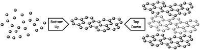 | ||
| Fig. 2 A schematic of ‘bottom-up’ and ‘top-down’ graphene synthesis. | ||
3.1 Top-down methods
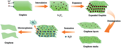
More recently electrochemical strategies have included expanding the graphite electrode in situ, followed by exfoliation of the electrode using sonication.79,80 This expansion has been achieved by intercalation of lithium salts to form graphite intercalation compounds (GICs). Sonication acts to separate the layers by injecting thermal shock into the material through ultrasonic cavitation.81 Sonication of lithium salt intercalated graphite in a mixed solvent of dimethylformamide (DMF) and propylene carbonate has been reported to give >70% few-layer graphene,79 while ∼80% few-layer graphene has been reported for sonication in water,80 where lithium and water react to form hydrogen gas which is thought to further aid exfoliation (Fig. 3).
The effect of thermal expansion of GICs was reported as early as 1916 for heating graphite–bromine intercalation compounds,85 but marked interest in the field did not begin until the late 1960s, when foils of exfoliated graphite were designed as gasket and sealant materials.86 Heating of GICs generally causes thermal decomposition of the intercalates into gaseous species that push the layers apart. ‘Expanded graphite’, also known as ‘exfoliated graphite’, has many industrial applications such as thermal insulators and composite filler materials, and more recently has been considered as a precursor for graphene.86 The most common method for expanded graphite formation is via the exposure of graphite to strong acids to yield a GIC (often graphite bisulfate) which is then exfoliated by rapid thermal heating or, more recently, by microwave radiation.87 Mono- to few-layer graphene has been reported for expanded graphite ground in ethanol,88 or sonicated in NMP (Fig. 4),89 while repeated cycles of intercalation–exfoliation followed by sonication in DMF has been shown to yield over 50% mono- and bi-layer graphene.90 Other examples of GICs designed for thermal exfoliation include graphite co-intercalated with iron chloride (FeCl3) and nitromethane (CH3NO2),91 and graphite intercalated with ionic liquid crystals (ILC).92 In the former iron chloride is used to promote the intercalation of nitromethane, which decomposes at relatively low temperatures (∼100 °C) under microwave radiation, while in the latter mild heating is used to promote ILC intercalation due to their reduced viscosity at higher temperatures, and stronger heating (to 700 °C) is used to induce thermal decomposition. Based on a similar principle supercritical carbon dioxide has been used to exfoliate graphite based on intercalation of the CO2 in the supercritical phase followed by rapid expansion upon depressurization to form gaseous CO2 which forces the graphitic layers apart.93
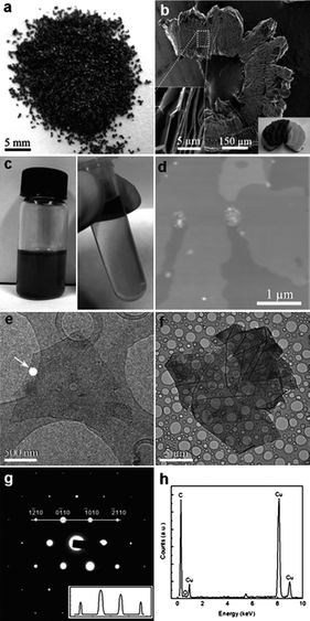 | ||
| Fig. 4 Graphene from liquid phase exfoliation of worm-like exfoliated graphite (WEG). Photograph of WEG (a), SEM image of WEG (b), uniform dispersions upon sonication (c, left) and centrifugation (c, right), AFM image (d) and TEM image (e) of the monolayer graphene sheets, TEM image of the monolayer graphene sheets (f), electron diffraction from the white spot marked in (e) (g) and EDX spectrum of the graphene sheet in (f) (h).89 | ||
Dispersions with high concentrations of graphene are advantageous as they require smaller volumes of potentially expensive and hazardous solvents, so several approaches have been tried to increase graphene concentration. Simply increasing sonication time or sonicating with a sonic probe rather than a sonic bath have been shown to increase the concentration of graphene in solution.96,97 Many of the best solvents for graphene have high boiling points, for example NMP has a boiling point >200 °C, which makes removal difficult when forming films or coatings from solution. Extended sonication (48 hours) in ‘poor’ but low boiling point solvents has achieved graphite concentrations up to 0.5 mg mL−1,98 which is approximately half the value reported for NMP after 460 hours of sonication.96 It should be noted that while prolonged sonication time improves the dispersibility of graphene the increase in concentration has been shown to be accompanied by a decrease in flake size and an increase in defect concentration.96
Another strategy for exfoliation of unmodified graphite flakes involves sonication in aqueous surfactant solutions,99,100 which has the advantage of avoiding expensive and often harmful solvents. In addition the surfactants can prevent re-aggregation of the graphene due to the repulsive potential barrier between surfactant-coated sheets, the importance of which has been studied with regard to graphene dispersion for both ionic and non-ionic surfactants.101 Concentrations up to 0.3 mg mL−1 have been reported for graphene sonicated in sodium cholate solutions for ∼400 hours,100 but as with electrochemical exfoliation in surfactant solutions, this method has the disadvantage that surfactants are difficult to remove and can affect properties.
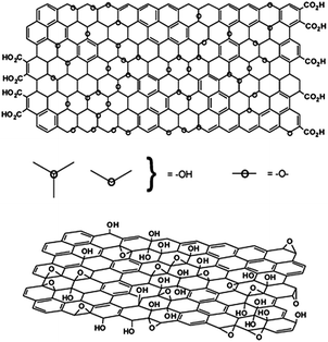 | ||
| Fig. 5 Variations in the Lerf–Klinowski model indicating ambiguity regarding the presence (top) or absence (bottom) of carboxylic acids on the periphery of the basal plane of the graphitic platelets of GO.109 | ||
Graphene is obtained by exfoliation of graphite oxide into graphene oxide (GO), followed by reduction of graphene oxide to produce graphene. The resulting material is generally termed ‘reduced graphene oxide’ (rGO) or ‘functionalised graphene’ rather than ‘graphene’ as complete reduction has not yet been achieved. Graphite oxide is exfoliated more readily than graphite, using thermal treatments or via sonication in water,109 and the graphene oxide produced can then be reduced using either thermal or chemical methods. The different methods of reduction have been reviewed recently and will not be discussed here.113 Graphene oxide is electrically insulating due to the functional groups disrupting the sp2 hybridisation of the graphene layers, so efficient reduction is an important step in restoring desirable electrical properties of the material. One of the key issues surrounding chemical reduction is that GO sheets become less hydrophilic upon reduction and tend to aggregate and precipitate,114 making complete reduction difficult. It should be noted that even if complete reduction is achieved the properties of rGO are unlikely to match those of graphene due to the high levels of defects induced in the harsh oxidation processes used to produce graphite oxide.
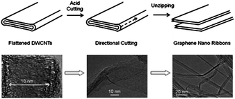 | ||
| Fig. 6 A schematic of directional unzipping of flattened carbon nanotubes (top) and corresponding TEM images (bottom).126 | ||
3.2 Bottom-up methods
 | ||
| Fig. 7 Large scale graphene films grown on 4H-SiC. Optical microscope image of a millimeter-sized carbon film (a), Raman mapping of the intensity of G peaks; the image scale is 20 μm × 20 μm (b), STM image showing the irradiated area is covered by atomic flat graphene flakes (c) and atomic resolution image for the well organised graphene (d).132 | ||
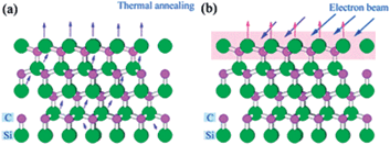 | ||
| Fig. 8 Schematic description of Si atom sublimation in Si-terminated 4H-SiC under thermal annealing process (a) and pulsed electron beam irradiation process (b).132 | ||
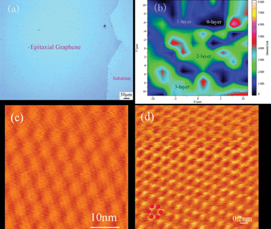
Generally hexagonal phase silicon carbide (4H-SiC or 6H-SiC) has been used for graphene synthesis although more recently growth over cubic phase SiC has also been demonstrated.133–135 Graphene forms nearly commensurate structures with both the silicon-rich SiC(0001) and carbon rich SiC(000![[1 with combining macron]](https://www.rsc.org/images/entities/char_0031_0304.gif) ) faces of hexagonal SiC, and has been grown on both.136 While in both cases there is an interface layer between the graphene and ‘bulk’ SiC, a marked difference has been observed between the structures of graphene grown on the different faces, where graphene formation on the Si-rich face is the most studied, and hence well understood, of the two.137 For the Si-rich face graphene grows in a single orientation (rotated 30° with respect to SiC) and exhibits regular Bernal stacking.138 The graphene produced is relatively high quality, although the uniformity of graphene for ≤2 layers is rather poor due to surface pits that form as a result of steps in the SiC surface.139 In contrast graphene formed on the C-rich face exhibits rotational stacking, where each of the rotations forms a commensurate structure with either SiC or the underlying graphene layer.136,140 This rotational misalignment is thought to be the origin of the higher electrical conductivity measured for graphene on the C-rich face compared with the Si-face, due to the rotation causing electronic decoupling of the layers, resulting in monolayer-like properties for the stacked multilayer.141 Growth on the C-rich face occurs at lower temperatures than for the Si-rich face and the rate of growth decreases to a lesser extent with graphene thickness, meaning graphene with >10 layers is common for C-face SiC.137 Like the Si-rich face, the C-rich face is sensitive to the SiC surface, and the presence of unintentional oxide (Si2O3) has been shown to affect graphene uniformity.142 In addition restricted graphene grain sizes have been observed for material grown on the C-rich face; attributed to the lower growth temperatures used.137
) faces of hexagonal SiC, and has been grown on both.136 While in both cases there is an interface layer between the graphene and ‘bulk’ SiC, a marked difference has been observed between the structures of graphene grown on the different faces, where graphene formation on the Si-rich face is the most studied, and hence well understood, of the two.137 For the Si-rich face graphene grows in a single orientation (rotated 30° with respect to SiC) and exhibits regular Bernal stacking.138 The graphene produced is relatively high quality, although the uniformity of graphene for ≤2 layers is rather poor due to surface pits that form as a result of steps in the SiC surface.139 In contrast graphene formed on the C-rich face exhibits rotational stacking, where each of the rotations forms a commensurate structure with either SiC or the underlying graphene layer.136,140 This rotational misalignment is thought to be the origin of the higher electrical conductivity measured for graphene on the C-rich face compared with the Si-face, due to the rotation causing electronic decoupling of the layers, resulting in monolayer-like properties for the stacked multilayer.141 Growth on the C-rich face occurs at lower temperatures than for the Si-rich face and the rate of growth decreases to a lesser extent with graphene thickness, meaning graphene with >10 layers is common for C-face SiC.137 Like the Si-rich face, the C-rich face is sensitive to the SiC surface, and the presence of unintentional oxide (Si2O3) has been shown to affect graphene uniformity.142 In addition restricted graphene grain sizes have been observed for material grown on the C-rich face; attributed to the lower growth temperatures used.137
The demanding growth conditions are one of the key challenges of growing graphene on SiC. One solution that allows lower temperature conditions (700–800 °C) is nickel catalysed growth, where a thin layer of nickel is deposited on the surface of the SiC prior to annealing, and graphene forms on the upper nickel surface.143–146 While this method uses lower temperatures, it has the additional cost of using a transition metal and requires transfer to insulating substrates for use in electronic applications.
Graphene growth on SiC is generally for wafer-based applications, such as electronic devices or components, and as such it is not generally necessary to remove the graphene from the underlying substrate. However the transfer of graphene directly from SiC has been demonstrated,147,148 although is hindered by the strong interactions between the two materials.149 SiC is commercially available but expensive, particularly for large area films, so a hurdle for their use in commercial applications will be reducing this cost. Cubic SiC is cheaper to produce133 so may pose a solution, but graphene growth on this phase is still in its infancy.
3.2.2.1 Growth on metals. Chemical vapour deposition (CVD), where graphene is formed by the high temperature pyrolysis of carbon containing gases, has been widely used to grow graphene films on transition metal substrates and represents a very active area of graphene research. CVD graphene growth can be categorised as proceeding through either surface-catalysed or segregation methods depending on the metal. For surface catalysed reactions the decomposition of the carbon containing species and graphene formation occur at the metal surface, and growth can be described as “self-limiting” to monolayer graphene as the surface is pacified once covered. For segregation, graphene forms via the diffusion of carbon dissolved in the bulk metal to the metal surface, which generally occurs upon cooling due to the reduced solubility of carbon in metals at lower temperatures. The number of graphene layers produced by segregation depends on various factors including the amount of carbon dissolved and the rate of cooling.150,151
Graphene growth has been demonstrated on a wide range of metals, including group 8–10 transition metals (Fe,152,153 Ru,154–156 Co,157–160 Rh,161,162 Ir,163,164 Ni,19,165–170 Pd,171,172 Pt,173,174 Cu,175–181 Au182) and a number of alloys (Co–Ni,183–186 Au–Ni,187 Ni–Mo,188 stainless steel189,190). The optimum conditions for CVD growth vary depending on the metal, with different factors (pressure, temperature and carbon exposure) impacting graphene quality and thickness to different extents depending on the system. In addition the strength of graphene–metal interaction differs, which can impact the degree of graphene rippling, the sensitivity of graphene to defects in the metal surface, and the ease of graphene transfer to arbitrary substrates. While there are a number of fundamental properties that affect the potential of a metal for use in large-scale CVD growth, ultimately cost and availability are likely to be some of the most important factors, particularly as the metal is generally etched during graphene transfer (Fig. 9). To date copper and nickel have received the most attention, with graphene films of diagonal lengths up to 30 inches having been grown and transferred from polycrystalline copper foils.67 Graphene growth on copper is thought to proceed via the surface catalysed mechanism, resulting in monolayer graphene growth for a range of reaction conditions,176 whereas growth on nickel proceeds via segregation191 and is more difficult to control – although it has the advantage of not requiring UHV conditions, as used in the majority of syntheses of graphene on copper.
 | ||
| Fig. 9 A schematic of graphene growth and removal from metal surfaces. | ||
Continuous graphene growth has been observed over the metal grain boundaries of polycrystalline films of both copper192 and nickel.167 This is important as although studying growth over single crystal metals can provide valuable mechanistic information, the difficulty in growing large-area single crystal metals prohibits their use in the production of large-scale graphene films. Instead polycrystalline metal films, in the form of polycrystalline foils or thin films deposited by sputter coating or electron beam evaporation, are likely to be the future for large area CVD grown graphene films. One of the key challenges that faces growth over polycrystalline films is the behaviour of graphene at the grain boundaries, where even if growth over grain boundaries is continuous, the sites have been shown to lead to defects such as nucleation of multi-layer graphene, which degrade the properties of the graphene films.166 Work is underway to engineer high quality polycrystalline films by careful control of the metal deposition and annealing conditions.193
CVD growth over metals has the disadvantage that harsh growth conditions are required, especially for the metals that utilise UHV conditions. Improving these conditions can be complicated, for example while growth over copper has been demonstrated under atmospheric pressure conditions, patches of multi-layer graphene were observed on the surface suggesting that unlike in UHV conditions, the growth is not self limiting to monolayer graphene.194 Attempts have also been made to reduce the temperatures required for growth, for example using carbon sources with lower decompositions temperatures.195,196 The different conditions for graphene growth over polycrystalline metals have been recently reviewed elsewhere.197
Metal films are electrically conducting so to enable the use of CVD grown graphene films in a number of electronic applications, transfer of graphene films onto insulating substrates is required. The transfer of graphene from different metals has been demonstrated using a variety of chemical etchants to release the graphene from the metal.197 This process can be damaging to the films, so often a polymer support is used to prevent the films cracking.198,199 The general method for this is to spin coat the polymer onto the graphene surface, etch the underlying metal, place the graphene on the new substrate, and dissolve the polymer to yield naked graphene. Furthermore graphene transfer onto flexible substrates has been demonstrated using industrially compatible techniques such as hot press lamination200 and roll-to-roll transfer,201 allowing the transfer of large area films. As for transfer using a polymer stamp these processes also require etching of the metal, which is both costly and wasteful. Recently transfer via electrochemical delamination has been presented where only a small amount of the metal is etched, allowing the copper substrate to be reused in subsequent growth reactions.202
It should be noted that in addition to CVD growth via vapours introduced into the furnace during the reaction, graphene has been grown from solid carbon sources positioned on-top of the substrate, for example the transition metal mediated graphitisation of films of amorphous carbon,203,204 nanodiamond,205 polymers,206,207 and self-assembled monolayers (SAMs).208 The growth of monolayer graphene on copper has even been achieved by thermally decomposing cookies, chocolate, grass, and cockroach legs (Fig. 10).209
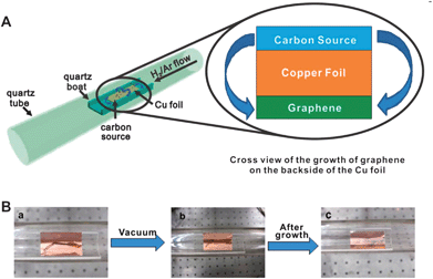 | ||
| Fig. 10 Diagram of the experimental apparatus for the growth of graphene from food, insects, or waste in a tube furnace (A), and growth of graphene from a cockroach leg (B) showing one roach leg on top of the Cu foil (a), the roach leg under vacuum (b) and the residual roach leg after annealing at 1050 °C for 15 min (c). The pristine graphene grew on the bottom side of the Cu film (not shown).209 Reproduced with permission of the American Chemical Society. | ||
3.2.2.2 Substrate free. Besides growing graphene films, CVD has been also used to synthesise graphene nanosheets. Substrate free synthesis has the advantage that specific substrates do not need to be purchased or prepared and that the removal of graphene from the substrate is not required. Furthermore as the material is collected outside the furnace, graphene can be produced via continuous rather than batch processing. An early example of substrate free growth is the work by Dato et al.,210,211 where the growth of single and bilayer graphene has been reported via atmospheric pressure, microwave enhanced CVD of ethanol. More recently a route to produce few-layer graphene via substrate free CVD has been demonstrated using thermal decomposition of sodium ethoxide in ethanol.212 Both methods yield large quantities of graphene.
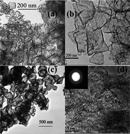 | ||
| Fig. 11 TEM images of few-layer graphene produced by burning magnesium metal in dry ice. Graphenes with an average length of 50–100 nm (a), larger size graphene sheets with an average length of 300 nm (b), crystalline graphenes with an average length of 200 nm (c), high-resolution TEM image of few-layer graphenes, with the number of layers ranging from 3–7 (d), and electron diffraction pattern of graphenes (inset).214 | ||
Recently Xu et al. have presented an approach to graphene nanosheet synthesis that seems to involve both bottom-up and top-down approaches.217 In this work graphite is produced via high temperature synthesis and carbonisation of metal phthalocyanine in a microwave-heater at 450 °C, then exfoliated to graphene by rapid cooling.
The bottom-up synthesis of transparent graphene films has been demonstrated by heating electrically insulating substrates (quartz, SiO2/Si) spin coated with solutions of polyaromatic hydrocarbons (PAHs) in chloroform to 1100 °C to cause fusion of the molecules and result in graphene films of varying thickness depending on the concentration of PAH solution.218 PAH chemistry has been utilised to synthesise structures containing as many as 222 carbon units (37 benzene units) with disk diameters of 3.2 nm, termed ‘nanographene’,219 in addition to the formation of graphene nanoribbons using similar methodologies.220
4 Conclusion
The controlled, large scale synthesis of high quality graphene still remains a challenge, although understanding of the processing techniques required to achieve this goal is growing as the body of graphene-based research is expanding rapidly. The methods currently used for graphene synthesis all have their advantages and disadvantages, and which process is used should be guided by the end-application of the material. While single layer graphene sheets have been produced using methods amenable to scale, the major products of most large-scale methods are few-layer graphene or thin graphite sheets. Still many of these materials have shown promise in applications and fill an unoccupied niche, which will help to drive further research in the area. An example of this is the use of wrinkled graphene in conducting inks, which are due to appear on store shelves in a new kind of anti-theft packaging.221 Here graphene has filled the gap between traditional polymer and carbon based films which are too poorly conducting, and expensive silver inks that are difficult to process. Similarly the ambition of forming flexible electronics, an application for which graphene is a major contender, increases the chances of seeing graphene in commercial devices. The future of graphene and some of the graphene-like materials produced in the pursuit of graphene is difficult to predict, but it's likely that they are going to play a very important part in many applications.Notes and references
- K. S. Novoselov, A. K. Geim, S. V. Morozov, D. Jiang, Y. Zhang, S. V. Dubonos, I. V. Grigorieva and A. A. Firsov, Science, 2004, 306, 666–669 CrossRef CAS.
- A. K. Geim and K. S. Novoselov, Nat. Mater., 2007, 6, 183–191 CrossRef CAS.
- B. Partoens and F. M. Peeters, Phys. Rev. B: Condens. Matter Mater. Phys., 2006, 74, 075404 CrossRef.
- A. Fasolino, J. H. Los and M. I. Katsnelson, Nat. Mater., 2007, 6, 858–861 CrossRef CAS.
- J. C. Meyer, A. K. Geim, M. I. Katsnelson, K. S. Novoselov, T. J. Booth and S. Roth, Nature, 2007, 446, 60–63 CrossRef CAS.
- E. Stolyarova, K. T. Rim, S. Ryu, J. Maultzsch, P. Kim, L. E. Brus, T. F. Heinz, M. S. Hybertsen and G. W. Flynn, Proc. Natl. Acad. Sci. U. S. A., 2007, 104, 9209–9212 CrossRef CAS.
- K. F. Mak, J. Shan and T. F. Heinz, Phys. Rev. Lett., 2010, 104, 176404 CrossRef.
- S. Horiuchi, T. Gotou, M. Fuijwara, R. Sotoaka, M. Hirata, K. Kimoto, T. Asaka, T. Yokosawa, Y. Matsui, K. Watanabe and M. Sekita, Jpn. J. Appl. Phys., 2003, 42, L1073–L1076 CrossRef CAS.
- L. M. Malard, M. A. Pimenta, G. Dresselhaus and M. S. Dresselhaus, Phys. Rep., 2009, 473, 51–87 CrossRef CAS.
- X. Jia, J. Campos-Delgado, M. Terrones, V. Meunier and M. S. Dresselhaus, Nanoscale, 2011, 3, 86–95 RSC.
- C. N. R. Rao, A. K. Sood, K. S. Subrahmanyam and A. Govindaraj, Angew. Chem., Int. Ed., 2009, 48, 7752–7777 CrossRef CAS.
- M. Acik and Y. J. Chabal, Jpn. J. Appl. Phys., 2012, 51, 039201 CrossRef.
- D. Wei and Y. Liu, Adv. Mater., 2010, 22, 3225–3241 CrossRef CAS.
- S. Dutta and S. K. Pati, J. Mater. Chem., 2010, 20, 8207–8223 RSC.
- J. S. Bunch, S. S. Verbridge, J. S. Alden, A. M. van der Zande, J. M. Parpia, H. G. Craighead and P. L. McEuen, Nano Lett., 2008, 8, 2458–2462 CrossRef CAS.
- C. Lee, X. D. Wei, J. W. Kysar and J. Hone, Science, 2008, 321, 385–388 CrossRef CAS.
- A. A. Balandin, S. Ghosh, W. Z. Bao, I. Calizo, D. Teweldebrhan, F. Miao and C. N. Lau, Nano Lett., 2008, 8, 902–907 CrossRef CAS.
- R. R. Nair, P. Blake, A. N. Grigorenko, K. S. Novoselov, T. J. Booth, T. Stauber, N. M. R. Peres and A. K. Geim, Science, 2008, 320, 1308 CrossRef CAS.
- K. S. Kim, Y. Zhao, H. Jang, S. Y. Lee, J. M. Kim, K. S. Kim, J.-H. Ahn, P. Kim, J.-Y. Choi and B. H. Hong, Nature, 2009, 457, 706–710 CrossRef CAS.
- A. H. Castro Neto, F. Guinea, N. M. R. Peres, K. S. Novoselov and A. K. Geim, Rev. Mod. Phys., 2009, 81, 109–162 CrossRef CAS.
- C. N. Lau, W. Bao and J. Velasco Jr, Mater. Today, 2012, 15, 238–245 CrossRef CAS.
- K. I. Bolotin, K. J. Sikes, Z. Jiang, M. Klima, G. Fudenberg, J. Hone, P. Kim and H. L. Stormer, Solid State Commun., 2008, 146, 351–355 CrossRef CAS.
- X. Du, I. Skachko, A. Barker and E. Y. Andrei, Nat. Nanotechnol., 2008, 3, 491–495 CrossRef CAS.
- K. S. Novoselov, A. K. Geim, S. V. Morozov, D. Jiang, M. I. Katsnelson, I. V. Grigorieva, S. V. Dubonos and A. A. Firsov, Nature, 2005, 438, 197–200 CrossRef CAS.
- A. Shytov, M. Rudner, N. Gu, M. Katsnelson and L. Levitov, Solid State Commun., 2009, 149, 1087–1093 CrossRef CAS.
- F. Miao, S. Wijeratne, Y. Zhang, U. C. Coskun, W. Bao and C. N. Lau, Science, 2007, 317, 1530–1533 CrossRef CAS.
- S. Adam, E. H. Hwang, E. Rossi and S. Das Sarma, Solid State Commun., 2009, 149, 1072–1079 CrossRef CAS.
- A. M. Ilyin, E. A. Daineko and G. W. Beall, Phys. E., 2009, 42, 67–69 CrossRef CAS.
- G. Compagnini, F. Giannazzo, S. Sonde, V. Raineri and E. Rimini, Carbon, 2009, 47, 3201–3207 CrossRef CAS.
- H. S. Skulason, P. E. Gaskell and T. Szkopek, Nanotechnology, 2010, 21, 295709 CrossRef CAS.
- M. Klintenberg, S. Lebègue, C. Ortiz, B. Sanyal, J. Fransson and O. Eriksson, J. Phys.: Condens. Matter, 2009, 21, 335502 CrossRef CAS.
- A. Z. AlZahrani and G. P. Srivastava, J. Phys.: Condens. Matter, 2009, 21, 495503 CrossRef CAS.
- S. Ghosh, W. Bao, D. L. Nika, S. Subrina, E. P. Pokatilov, C. N. Lau and A. A. Balandin, Nat. Mater., 2010, 9, 555–558 CrossRef CAS.
- Y. Zhang and C. Pan, Diamond Relat. Mater., 2012, 24, 1–5 CrossRef CAS.
- S. Alwarappan, S. Boyapalle, A. Kumar, C.-Z. Li and S. Mohapatra, J. Phys. Chem. C, 2012, 116, 6556–6559 CAS.
- J. D. Roy-Mayhew, D. J. Bozym, C. Punckt and I. A. Aksay, ACS Nano, 2010, 4, 6203–6211 CrossRef CAS.
- H.-C. Wu, Y.-Y. Li and A. Sakoda, Int. J. Hydrogen Energy, 2010, 35, 4123–4130 CrossRef CAS.
- F. Schwierz, Nat. Nanotechnol., 2010, 5, 487–496 CrossRef CAS.
- Y. Huang, J. Liang and Y. Chen, Small, 2012, 8, 1805–1834 CrossRef CAS.
- M. H. Liang and L. J. Zhi, J. Mater. Chem., 2009, 19, 5871–5878 RSC.
- W. Wei, Y. Qingkai, P. Peng, L. Zhihong, B. Jiming and P. Shin-Shem, Nanotechnology, 2012, 23, 035603 CrossRef.
- D. A. C. Brownson and C. E. Banks, Analyst, 2010, 135, 2768–2778 RSC.
- L. Huang, Y. Huang, J. Liang, X. Wan and Y. Chen, Nano Res., 2011, 4, 675–684 CrossRef CAS.
- X. Huang, X. Y. Qi, F. Boey and H. Zhang, Chem. Soc. Rev., 2012, 41, 666–686 RSC.
- Y. X. Liu, X. C. Dong and P. Chen, Chem. Soc. Rev., 2012, 41, 2283–2307 RSC.
- H. Hibino, S. Tanabe, S. Mizuno and H. Kageshima, J. Phys. D: Appl. Phys., 2012, 45, 154008 CrossRef.
- Y.-M. Lin, C. Dimitrakopoulos, K. A. Jenkins, D. B. Farmer, H.-Y. Chiu, A. Grill and P. Avouris, Science, 2010, 327, 662 CrossRef CAS.
- Y.-M. Lin, A. Valdes-Garcia, S.-J. Han, D. B. Farmer, I. Meric, Y. Sun, Y. Wu, C. Dimitrakopoulos, A. Grill, P. Avouris and K. A. Jenkins, Science, 2011, 332, 1294–1297 CrossRef CAS.
- W. Choi, I. Lahiri, R. Seelaboyina and Y. S. Kang, Crit. Rev. Solid State Mater. Sci., 2010, 35, 52–71 CrossRef CAS.
- E. Kymakis, E. Stratakis, M. M. Stylianakis, E. Koudoumas and C. Fotakis, Thin Solid Films, 2011, 520, 1238–1241 CrossRef CAS.
- X. Lv, Y. Huang, Z. Liu, J. Tian, Y. Wang, Y. Ma, J. Liang, S. Fu, X. Wan and Y. Chen, Small, 2009, 5, 1682–1687 CrossRef CAS.
- V. H. Pham, T. V. Cuong, S. H. Hur, E. W. Shin, J. S. Kim, J. S. Chung and E. J. Kim, Carbon, 2010, 48, 1945–1951 CrossRef CAS.
- Z.-S. Wu, S. Pei, W. Ren, D. Tang, L. Gao, B. Liu, F. Li, C. Liu and H.-M. Cheng, Adv. Mater., 2009, 21, 1756–1760 CrossRef CAS.
- L. J. Cote, F. Kim and J. Huang, J. Am. Chem. Soc., 2008, 131, 1043–1049 CrossRef.
- P. Avouris and C. Dimitrakopoulos, Mater. Today, 2012, 15, 86–97 CrossRef CAS.
- T. Palacios, Nature, 2012, 483, S40–S41 CrossRef.
- M. I. Katsnelson, Mater. Today, 2007, 10, 20–27 CrossRef CAS.
- X. Wang, Y. Ouyang, L. Jiao, H. Wang, L. Xie, J. Wu, J. Guo and H. Dai, Nat. Nanotechnol., 2011, 6, 563–567 CrossRef CAS.
- Y. Zhang, T.-T. Tang, C. Girit, Z. Hao, M. C. Martin, A. Zettl, M. F. Crommie, Y. R. Shen and F. Wang, Nature, 2009, 459, 820–823 CrossRef CAS.
- V. M. Pereira, A. H. Castro Neto and N. M. R. Peres, Phys. Rev. B: Condens. Matter Mater. Phys., 2009, 80, 045401 CrossRef.
- R. Lv and M. Terrones, Mater. Lett., 2012, 78, 209–218 CrossRef CAS.
- D. Wei, Y. Liu, Y. Wang, H. Zhang, L. Huang and G. Yu, Nano Lett., 2009, 9, 1752–1758 CrossRef CAS.
- Z. Jin, J. Yao, C. Kittrell and J. M. Tour, ACS Nano, 2011, 5, 4112–4117 CrossRef CAS.
- M. Segal, Nat. Nanotechnol., 2009, 4, 612–614 CrossRef CAS.
- N. Savage, Nature, 2012, 483, S38–S39 CrossRef CAS.
- A. Kasry, M. A. Kuroda, G. J. Martyna, G. S. Tulevski and A. A. Bol, ACS Nano, 2010, 4, 3839–3844 CrossRef CAS.
- S. Bae, H. Kim, Y. Lee, X. Xu, J.-S. Park, Y. Zheng, J. Balakrishnan, T. Lei, H. R. Kim, Y. I. Song, Y.-J. Kim, K. S. Kim, B. Ozyilmaz, J.-H. Ahn, B. H. Hong and S. Iijima, Nat. Nanotechnol., 2010, 5, 574–578 CrossRef CAS.
- Y. Hernandez, M. Lotya, D. Rickard, S. D. Bergin and J. N. Coleman, Langmuir, 2009, 26, 3208–3213 CrossRef.
- Y. Si and E. T. Samulski, Nano Lett., 2008, 8, 1679–1682 CrossRef CAS.
- C. Liu, Z. Yu, D. Neff, A. Zhamu and B. Z. Jang, Nano Lett., 2010, 10, 4863–4868 CrossRef CAS.
- M. D. Stoller, S. J. Park, Y. W. Zhu, J. H. An and R. S. Ruoff, Nano Lett., 2008, 8, 3498–3502 CrossRef CAS.
- R. O. Brennan, J. Chem. Phys., 1952, 20, 40–48 CrossRef CAS.
- http://ec.europa.eu/enterprise/policies/raw-materials/critical/index_en.htm .
- M. Inagaki, in New Carbons – Control of Structure and Functions, Elsevier Science, Oxford, 2000, pp. 30–57 Search PubMed.
- G. Wang, B. Wang, J. Park, Y. Wang, B. Sun and J. Yao, Carbon, 2009, 47, 3242–3246 CrossRef CAS.
- C.-Y. Su, A.-Y. Lu, Y. Xu, F.-R. Chen, A. N. Khlobystov and L.-J. Li, ACS Nano, 2011, 5, 2332–2339 CrossRef CAS.
- J. M. Englert, J. Röhrl, C. D. Schmidt, R. Graupner, M. Hundhausen, F. Hauke and A. Hirsch, Adv. Mater., 2009, 21, 4265–4269 CrossRef CAS.
- D. A. C. Brownson, J. P. Metters, D. K. Kampouris and C. E. Banks, Electroanalysis, 2011, 23, 894–899 CrossRef CAS.
- J. Wang, K. K. Manga, Q. Bao and K. P. Loh, J. Am. Chem. Soc., 2011, 133, 8888–8891 CrossRef CAS.
- H. Huang, Y. Xia, X. Tao, J. Du, J. Fang, Y. Gan and W. Zhang, J. Mater. Chem., 2012, 22, 10452–10456 RSC.
- K. S. Suslick and G. J. Price, Annu. Rev. Mater. Sci., 1999, 29, 295–326 CrossRef CAS.
- C. Vallés, C. Drummond, H. Saadaoui, C. A. Furtado, M. He, O. Roubeau, L. Ortolani, M. Monthioux and A. Pénicaud, J. Am. Chem. Soc., 2008, 130, 15802–15804 CrossRef.
- X. Li, G. Zhang, X. Bai, X. Sun, X. Wang, E. Wang and H. Dai, Nat. Nanotechnol., 2008, 3, 538–542 CrossRef CAS.
- L. M. Viculis, J. J. Mack, O. M. Mayer, H. T. Hahn and R. B. Kaner, J. Mater. Chem., 2005, 15, 974–978 RSC.
- J. W. Aylesworth, US Pat., 1916, 1191383.
- D. D. L. Chung, J. Mater. Sci., 1987, 22, 4190–4198 CrossRef CAS.
- T. Wei, Z. Fan, G. Luo, C. Zheng and D. Xie, Carbon, 2009, 47, 337–339 CrossRef CAS.
- S. Malik, A. Vijayaraghavan, R. Erni, K. Ariga, I. Khalakhan and J. P. Hill, Nanoscale, 2010, 2, 2139–2143 RSC.
- W. Gu, W. Zhang, X. Li, H. Zhu, J. Wei, Z. Li, Q. Shu, C. Wang, K. Wang, W. Shen, F. Kang and D. Wu, J. Mater. Chem., 2009, 19, 3367–3369 RSC.
- S. R. Dhakate, N. Chauhan, S. Sharma, J. Tawale, S. Singh, P. D. Sahare and R. B. Mathur, Carbon, 2011, 49, 1946–1954 CrossRef CAS.
- W. Fu, J. Kiggans, S. H. Overbury, V. Schwartz and C. Liang, Chem. Commun., 2011, 47, 5265–5267 RSC.
- A. Safavi, M. Tohidi, F. A. Mahyari and H. Shahbaazi, J. Mater. Chem., 2012, 22, 3825–3831 RSC.
- N.-W. Pu, C.-A. Wang, Y. Sung, Y.-M. Liu and M.-D. Ger, Mater. Lett., 2009, 63, 1987–1989 CrossRef CAS.
- P. Blake, P. D. Brimicombe, R. R. Nair, T. J. Booth, D. Jiang, F. Schedin, L. A. Ponomarenko, S. V. Morozov, H. F. Gleeson, E. W. Hill, A. K. Geim and K. S. Novoselov, Nano Lett., 2008, 8, 1704–1708 CrossRef.
- Y. Hernandez, V. Nicolosi, M. Lotya, F. M. Blighe, Z. Sun, S. De, I. T. McGovern, B. Holland, M. Byrne, Y. K. Gun'ko, J. J. Boland, P. Niraj, G. Duesberg, S. Krishnamurthy, R. Goodhue, J. Hutchison, V. Scardaci, A. C. Ferrari and J. N. Coleman, Nat. Nanotechnol., 2008, 3, 563–568 CrossRef CAS.
- U. Khan, A. O'Neill, M. Lotya, S. De and J. N. Coleman, Small, 2010, 6, 864–871 CrossRef CAS.
- U. Khan, H. Porwal, A. O'Neill, K. Nawaz, P. May and J. N. Coleman, Langmuir, 2011, 27, 9077–9082 CrossRef CAS.
- A. O'Neill, U. Khan, P. N. Nirmalraj, J. Boland and J. N. Coleman, J. Phys. Chem. C, 2011, 115, 5422–5428 CAS.
- M. Lotya, Y. Hernandez, P. J. King, R. J. Smith, V. Nicolosi, L. S. Karlsson, F. M. Blighe, S. De, Z. Wang, I. T. McGovern, G. S. Duesberg and J. N. Coleman, J. Am. Chem. Soc., 2009, 131, 3611–3620 CrossRef CAS.
- M. Lotya, P. J. King, U. Khan, S. De and J. N. Coleman, ACS Nano, 2010, 4, 3155–3162 CrossRef CAS.
- J. S. Ronan, L. Mustafa and N. C. Jonathan, New J. Phys., 2010, 12, 125008 CrossRef.
- L. Staudenmaier, Ber. Dtsch. Chem. Ges., 1898, 31, 1481–1487 CrossRef CAS.
- B. C. Brodie, Philos. Trans. R. Soc. London, 1859, 149, 249–259 CrossRef.
- W. S. Hummers and R. E. Offeman, J. Am. Chem. Soc., 1958, 80, 1339 CrossRef CAS.
- D. C. Marcano, D. V. Kosynkin, J. M. Berlin, A. Sinitskii, Z. Sun, A. Slesarev, L. B. Alemany, W. Lu and J. M. Tour, ACS Nano, 2010, 4, 4806–4814 CrossRef CAS.
- N. I. Kovtyukhova, P. J. Ollivier, B. R. Martin, T. E. Mallouk, S. A. Chizhik, E. V. Buzaneva and A. D. Gorchinskiy, Chem. Mater., 1999, 11, 771–778 CrossRef CAS.
- G. Shao, Y. Lu, F. Wu, C. Yang, F. Zeng and Q. Wu, J. Mater. Sci., 2012, 47, 4400–4409 CrossRef CAS.
- S. Lee, J. Oh, R. S. Ruoff and S. Park, Carbon, 2012, 50, 1442–1444 CrossRef CAS.
- D. R. Dreyer, S. Park, C. W. Bielawski and R. S. Ruoff, Chem. Soc. Rev., 2010, 39, 228–240 RSC.
- A. Lerf, H. He, M. Forster and J. Klinowski, J. Phys. Chem. B, 1998, 102, 4477–4482 CrossRef CAS.
- H. He, J. Klinowski, M. Forster and A. Lerf, Chem. Phys. Lett., 1998, 287, 53–56 CrossRef CAS.
- A. Buchsteiner, A. Lerf and J. Pieper, J. Phys. Chem. B, 2006, 110, 22328–22338 CrossRef CAS.
- S. Pei and H.-M. Cheng, Carbon, 2012, 50, 3210–3228 CrossRef CAS.
- S. Stankovich, D. A. Dikin, R. D. Piner, K. A. Kohlhaas, A. Kleinhammes, Y. Jia, Y. Wu, S. T. Nguyen and R. S. Ruoff, Carbon, 2007, 45, 1558–1565 CrossRef CAS.
- S. Farhat and C. D. Scott, J. Nanosci. Nanotechnol., 2006, 6, 1189–1210 CrossRef CAS.
- K. S. Subrahmanyam, L. S. Panchakarla, A. Govindaraj and C. N. R. Rao, J. Phys. Chem. C, 2009, 113, 4257–4259 CAS.
- Y. Chen, H. Zhao, L. Sheng, L. Yu, K. An, J. Xu, Y. Ando and X. Zhao, Chem. Phys. Lett., 2012, 538, 72–76 CrossRef CAS.
- B. Shen, J. Ding, X. Yan, W. Feng, J. Li and Q. Xue, Appl. Surf. Sci., 2012, 258, 4523–4531 CrossRef CAS.
- D. V. Kosynkin, A. L. Higginbotham, A. Sinitskii, J. R. Lomeda, A. Dimiev, B. K. Price and J. M. Tour, Nature, 2009, 458, 872–875 CrossRef CAS.
- P. Kumar, L. S. Panchakarla and C. N. R. Rao, Nanoscale, 2011, 3, 2127–2129 RSC.
- L. Jiao, L. Zhang, X. Wang, G. Diankov and H. Dai, Nature, 2009, 458, 877–880 CrossRef CAS.
- L. Valentini, Diamond Relat. Mater., 2011, 20, 445–448 CrossRef CAS.
- K. Nakada, M. Fujita, G. Dresselhaus and M. S. Dresselhaus, Phys. Rev. B: Condens. Matter, 1996, 54, 17954–17961 CrossRef CAS.
- L. Xie, H. Wang, C. Jin, X. Wang, L. Jiao, K. Suenaga and H. Dai, J. Am. Chem. Soc., 2011, 133, 10394–10397 CrossRef CAS.
- S. Cho, K. Kikuchi and A. Kawasaki, Carbon, 2011, 49, 3865–3872 CrossRef CAS.
- Y.-R. Kang, Y.-L. Li and M.-Y. Deng, J. Mater. Chem., 2012, 22, 16283–16287 RSC.
- P. Sutter, Nat. Mater., 2009, 8, 171–172 CrossRef CAS.
- K. V. Emtsev, A. Bostwick, K. Horn, J. Jobst, G. L. Kellogg, L. Ley, J. L. McChesney, T. Ohta, S. A. Reshanov, J. Rohrl, E. Rotenberg, A. K. Schmid, D. Waldmann, H. B. Weber and T. Seyller, Nat. Mater., 2009, 8, 203–207 CrossRef CAS.
- C. Virojanadara, M. Syvaejarvi, R. Yakimova, L. I. Johansson, A. A. Zakharov and T. Balasubramanian, Phys. Rev. B: Condens. Matter Mater. Phys., 2008, 78, 245403 CrossRef.
- Luxmi, N. Srivastava, R. M. Feenstra and P. J. Fisher, J. Vac. Sci. Technol., B: Microelectron. Nanometer Struct.–Process., Meas., Phenom., 2010, 28, C5C1 CrossRef CAS.
- R. M. Tromp and J. B. Hannon, Phys. Rev. Lett., 2009, 102, 106104 CrossRef CAS.
- Q. Huang, X. Chen, J. Liu, W. Wang, G. Wang, W. Wang, R. Yang, Y. Liu and L. Guo, Chem. Commun., 2010, 46, 4917–4919 RSC.
- V. Y. Aristov, G. Urbanik, K. Kummer, D. V. Vyalikh, O. V. Molodtsova, A. B. Preobrajenski, A. A. Zakharov, C. Hess, T. Haenke, B. Buechner, I. Vobornik, J. Fujii, G. Panaccione, Y. A. Ossipyan and M. Knupfer, Nano Lett., 2010, 10, 992–995 CrossRef CAS.
- A. Ouerghi, A. Balan, C. Castelli, M. Picher, R. Belkhou, M. Eddrief, M. G. Silly, M. Marangolo, A. Shukla and F. Sirotti, Appl. Phys. Lett., 2012, 101, 021603–021605 CrossRef.
- A. Ouerghi, M. Marangolo, R. Belkhou, S. El Moussaoui, M. G. Silly, M. Eddrief, L. Largeau, M. Portail, B. Fain and F. Sirotti, Phys. Rev. B: Condens. Matter Mater. Phys., 2010, 82, 125445 CrossRef.
- J. Hass, W. A. de Heer and E. H. Conrad, J. Phys.: Condens. Matter, 2008, 20, 323202 CrossRef.
- N. Srivastava, H. Guowei, Luxmi, P. C. Mende, R. M. Feenstra and S. Yugang, J. Phys. D: Appl. Phys., 2012, 45, 154001 CrossRef.
- C. Riedl, C. Coletti and U. Starke, J. Phys. D: Appl. Phys., 2010, 43, 374009 CrossRef.
- J. B. Hannon and R. M. Tromp, Phys. Rev. B: Condens. Matter Mater. Phys., 2008, 77, 241404 CrossRef.
- J. Hicks, K. Shepperd, F. Wang and E. H. Conrad, J. Phys. D: Appl. Phys., 2012, 45, 154002 CrossRef.
- E. J. Mele, J. Phys. D: Appl. Phys., 2012, 45, 154004 CrossRef.
- Luxmi, N. Srivastava, G. He, R. M. Feenstra and P. J. Fisher, Phys. Rev. B: Condens. Matter Mater. Phys., 2010, 82, 235406 CrossRef.
- Z.-Y. Juang, C.-Y. Wu, C.-W. Lo, W.-Y. Chen, C.-F. Huang, J.-C. Hwang, F.-R. Chen, K.-C. Leou and C.-H. Tsai, Carbon, 2009, 47, 2026–2031 CrossRef CAS.
- A. A. Woodworth and C. D. Stinespring, Carbon, 2010, 48, 1999–2003 CrossRef CAS.
- T. Yoneda, M. Shibuya, K. Mitsuhara, A. Visikovskiy, Y. Hoshino and Y. Kido, Surf. Sci., 2010, 604, 1509–1515 CrossRef CAS.
- C. Y. Kang, L. L. Fan, S. Chen, Z. L. Liu, P. S. Xu and C. W. Zou, Appl. Phys. Lett., 2012, 100, 251604–251605 CrossRef.
- J. D. Caldwell, T. J. Anderson, J. C. Culbertson, G. G. Jernigan, K. D. Hobart, F. J. Kub, M. J. Tadjer, J. L. Tedesco, J. K. Hite, M. A. Mastro, R. L. Myers-Ward, C. R. Eddy, P. M. Campbell and D. K. Gaskill, ACS Nano, 2010, 4, 1108–1114 CrossRef CAS.
- S. Unarunotai, Y. Murata, C. E. Chialvo, H.-s. Kim, S. MacLaren, N. Mason, I. Petrov and J. A. Rogers, Appl. Phys. Lett., 2009, 95, 202101–202103 CrossRef.
- F. Varchon, R. Feng, J. Hass, X. Li, B. N. Nguyen, C. Naud, P. Mallet, J. Y. Veuillen, C. Berger, E. H. Conrad and L. Magaud, Phys. Rev. Lett., 2007, 99, 126805 CrossRef CAS.
- J. Wintterlin and M. L. Bocquet, Surf. Sci., 2009, 603, 1841–1852 CrossRef CAS.
- M. Batzill, Surf. Sci. Rep., 2012, 67, 83–115 CrossRef CAS.
- H. An, W.-J. Lee and J. Jung, Curr. Appl. Phys., 2011, 11, S81–S85 CrossRef.
- D. Kondo, K. Yagi, M. Sato, M. Nihei, Y. Awano, S. Sato and N. Yokoyama, Chem. Phys. Lett., 2011, 514, 294–300 CrossRef CAS.
- E. Sutter, P. Albrecht and P. Sutter, Appl. Phys. Lett., 2009, 95, 133109 CrossRef.
- P. W. Sutter, P. M. Albrecht and E. A. Sutter, Appl. Phys. Lett., 2010, 97, 213101 CrossRef.
- E. Sutter, P. Albrecht, F. E. Camino and P. Sutter, Carbon, 2010, 48, 4414–4420 CrossRef CAS.
- S. M. Wang, Y. H. Pei, X. Wang, H. Wang, Q. N. Meng, H. W. Tian, X. L. Zheng, W. T. Zheng and Y. C. Liu, J. Phys. D: Appl. Phys., 2010, 43, 455402 CrossRef.
- M. E. Ramon, A. Gupta, C. Corbet, D. A. Ferrer, H. C. P. Movva, G. Carpenter, L. Colombo, G. Bourianoff, M. Doczy, D. Akinwande, E. Tutuc and S. K. Banerjee, ACS Nano, 2011, 5, 7198–7204 CrossRef CAS.
- N. Zhan, G. Wang and J. Liu, Appl. Phys. A: Mater. Sci. Process., 2011, 105, 341–345 CrossRef CAS.
- H. Ago, Y. Ito, N. Mizuta, K. Yoshida, B. Hu, C. M. Orofeo, M. Tsuji, K.-i. Ikeda and S. Mizuno, ACS Nano, 2010, 4, 7407–7414 CrossRef CAS.
- E. V. Rut'kov, A. V. Kuz'michev and N. R. Gall, Phys. Solid State, 2011, 53, 1092–1098 CrossRef CAS.
- S. Roth, J. Osterwalder and T. Greber, Surf. Sci., 2011, 605, L17–L19 CrossRef CAS.
- F. Mueller, S. Grandthyll, C. Zeitz, K. Jacobs, S. Huefner, S. Gsell and M. Schreck, Phys. Rev. B: Condens. Matter Mater. Phys., 2011, 84, 075472 CrossRef.
- C. Vo-Van, A. Kimouche, A. Reserbat-Plantey, O. Fruchart, P. Bayle-Guillemaud, N. Bendiab and J. Coraux, Appl. Phys. Lett., 2011, 98, 181903 CrossRef.
- A. Reina, X. Jia, J. Ho, D. Nezich, H. Son, V. Bulovic, M. S. Dresselhaus and J. Kong, Nano Lett., 2009, 9, 30–35 CrossRef CAS.
- A. Reina, S. Thiele, X. Jia, S. Bhaviripudi, M. S. Dresselhaus, J. A. Schaefer and J. Kong, Nano Res., 2009, 2, 509–516 CrossRef CAS.
- L. G. De Arco, Y. Zhang, C. W. Schlenker, K. Ryu, M. E. Thompson and C. Zhou, ACS Nano, 2010, 4, 2865–2873 CrossRef.
- Y. Zhang, L. Gomez, F. N. Ishikawa, A. Madaria, K. Ryu, C. Wang, A. Badmaev and C. Zhou, J. Phys. Chem. Lett., 2010, 1, 3101–3107 CrossRef CAS.
- S. J. Chae, F. Guenes, K. K. Kim, E. S. Kim, G. H. Han, S. M. Kim, H.-J. Shin, S.-M. Yoon, J.-Y. Choi, M. H. Park, C. W. Yang, D. Pribat and Y. H. Lee, Adv. Mater., 2009, 21, 2328–2333 CrossRef CAS.
- W. Liu, B. L. Jackson, J. Zhu, C.-Q. Miao, C.-H. Chung, Y.-J. Park, K. Sun, J. Woo and Y.-H. Xie, ACS Nano, 2010, 4, 3927–3932 CrossRef CAS.
- S.-Y. Kwon, C. V. Ciobanu, V. Petrova, V. B. Shenoy, J. Bareno, V. Gambin, I. Petrov and S. Kodambaka, Nano Lett., 2009, 9, 3985–3990 CrossRef CAS.
- Y. Murata, S. Nie, A. Ebnonnasir, E. Starodub, B. B. Kappes, K. F. McCarty, C. V. Ciobanu and S. Kodambaka, Phys. Rev. B: Condens. Matter Mater. Phys., 2012, 85, 205443 CrossRef.
- T. Gao, S. Xie, Y. Gao, M. Liu, Y. Chen, Y. Zhang and Z. Liu, ACS Nano, 2011, 5, 9194–9201 CrossRef CAS.
- B. J. Kang, J. H. Mun, C. Y. Hwang and B. J. Cho, J. Appl. Phys., 2009, 106, 104309 CrossRef.
- C. Mattevi, H. Kim and M. Chhowalla, J. Mater. Chem., 2011, 21, 3324–3334 RSC.
- X. Li, W. Cai, J. An, S. Kim, J. Nah, D. Yang, R. Piner, A. Velamakanni, I. Jung, E. Tutuc, S. K. Banerjee, L. Colombo and R. S. Ruoff, Science, 2009, 324, 1312–1314 CrossRef CAS.
- W. Liu, H. Li, C. Xu, Y. Khatami and K. Banerjee, Carbon, 2011, 49, 4122–4130 CrossRef CAS.
- X. Li, C. W. Magnuson, A. Venugopal, J. An, J. W. Suk, B. Han, M. Borysiak, W. Cai, A. Velamakanni, Y. Zhu, L. Fu, E. M. Vogel, E. Voelkl, L. Colombo and R. S. Ruoff, Nano Lett., 2010, 10, 4328–4334 CrossRef CAS.
- X. Li, C. W. Magnuson, A. Venugopal, R. M. Tromp, J. B. Hannon, E. M. Vogel, L. Colombo and R. S. Ruoff, J. Am. Chem. Soc., 2011, 133, 2816–2819 CrossRef CAS.
- Y. Lee, S. Bae, H. Jang, S. Jang, S.-E. Zhu, S. H. Sim, Y. I. Song, B. H. Hong and J.-H. Ahn, Nano Lett., 2010, 10, 490–493 CrossRef CAS.
- Z. Luo, Y. Lu, D. W. Singer, M. E. Berck, L. A. Somers, B. R. Goldsmith and A. T. C. Johnson, Chem. Mater., 2011, 23, 1441–1447 CrossRef CAS.
- T. Oznuluer, E. Pince, E. O. Polat, O. Balci, O. Salihoglu and C. Kocabas, Appl. Phys. Lett., 2011, 98, 183101 CrossRef.
- N. Liu, L. Fu, B. Dai, K. Yan, X. Liu, R. Zhao, Y. Zhang and Z. Liu, Nano Lett., 2011, 11, 297–303 CrossRef CAS.
- X. Liu, L. Fu, N. Liu, T. Gao, Y. Zhang, L. Liao and Z. Liu, J. Phys. Chem. C, 2011, 115, 11976–11982 CAS.
- S. Chen, L. Brown, M. Levendorf, W. Cai, S.-Y. Ju, J. Edgeworth, X. Li, C. W. Magnuson, A. Velamakanni, R. D. Piner, J. Kang, J. Park and R. S. Ruoff, ACS Nano, 2011, 5, 1321–1327 CrossRef CAS.
- S. Chen, W. Cai, R. D. Piner, J. W. Suk, Y. Wu, Y. Ren, J. Kang and R. S. Ruoff, Nano Lett., 2011, 11, 3519–3525 CrossRef CAS.
- R. S. Weatherup, B. C. Bayer, R. Blume, C. Ducati, C. Baehtz, R. Schlögl and S. Hofmann, Nano Lett., 2011, 11, 4154–4160 CrossRef CAS.
- B. Dai, L. Fu, Z. Zou, M. Wang, H. Xu, S. Wang and Z. Liu, Nat. Commun., 2011, 2, 522 CrossRef.
- R. John, A. Ashokreddy, C. Vijayan and T. Pradeep, Nanotechnology, 2011, 22, 165701 CrossRef.
- H. Gullapalli, A. L. M. Reddy, S. Kilpatrick, M. Dubey and P. M. Ajayan, Small, 2011, 7, 1697–1700 CrossRef CAS.
- L. Baraton, Z. He, C. S. Lee, J. L. Maurice, C. S. Cojocaru, Y. H. Lee and D. Pribat, in GraphITA 2011, ed. L. Ottaviano and V. Morandi, Springer, Berlin, Heidelberg, 2012, ch. 1, pp. 1–7 Search PubMed.
- Q. Yu, L. A. Jauregui, W. Wu, R. Colby, J. Tian, Z. Su, H. Cao, Z. Liu, D. Pandey, D. Wei, T. F. Chung, P. Peng, N. P. Guisinger, E. A. Stach, J. Bao, S.-S. Pei and Y. P. Chen, Nat. Mater., 2011, 10, 443–449 CrossRef CAS.
- S. Thiele, A. Reina, P. Healey, J. Kedzierski, P. Wyatt, P.-L. Hsu, C. Keast, J. Schaefer and J. Kong, Nanotechnology, 2010, 21, 015601 CrossRef.
- S. Bhaviripudi, X. Jia, M. S. Dresselhaus and J. Kong, Nano Lett., 2010, 10, 4128–4133 CrossRef CAS.
- S. Kumar, N. McEvoy, T. Lutz, G. P. Keeley, V. Nicolosi, C. P. Murray, W. J. Blau and G. S. Duesberg, Chem. Commun., 2010, 46, 1422–1424 RSC.
- B. Zhang, W. H. Lee, R. Piner, I. Kholmanov, Y. Wu, H. Li, H. Ji and R. S. Ruoff, ACS Nano, 2012, 6, 2471–2476 CrossRef CAS.
- R. S. Edwards and K. S. Coleman, Acc. Chem. Res., 2012 DOI:10.1021/ar3001266.
- X. Liang, B. A. Sperling, I. Calizo, G. Cheng, C. A. Hacker, Q. Zhang, Y. Obeng, K. Yan, H. Peng, Q. Li, X. Zhu, H. Yuan, A. R. H. Walker, Z. Liu, L.-m. Peng and C. A. Richter, ACS Nano, 2011, 5, 9144–9153 CrossRef.
- N. Liu, Z. Pan, L. Fu, C. Zhang, B. Dai and Z. Liu, Nano Res., 2011, 4, 996–1004 CrossRef CAS.
- V. P. Verma, S. Das, I. Lahiri and W. Choi, Appl. Phys. Lett., 2010, 96, 203108 CrossRef.
- Z.-Y. Juang, C.-Y. Wu, A.-Y. Lu, C.-Y. Su, K.-C. Leou, F.-R. Chen and C.-H. Tsai, Carbon, 2010, 48, 3169–3174 CrossRef CAS.
- Y. Wang, Y. Zheng, X. Xu, E. Dubuisson, Q. Bao, J. Lu and K. P. Loh, ACS Nano, 2011, 5, 9927–9933 CrossRef CAS.
- M. Zheng, K. Takei, B. Hsia, H. Fang, X. Zhang, N. Ferralis, H. Ko, Y.-L. Chueh, Y. Zhang, R. Maboudian and A. Javey, Appl. Phys. Lett., 2010, 96, 063110 CrossRef.
- H. Ji, Y. Hao, Y. Ren, M. Charlton, W. H. Lee, Q. Wu, H. Li, Y. Zhu, Y. Wu, R. Piner and R. S. Ruoff, ACS Nano, 2011, 5, 7656–7661 CrossRef CAS.
- J. M. Garcia, R. He, M. P. Jiang, P. Kim, L. N. Pfeiffer and A. Pinczuk, Carbon, 2011, 49, 1006–1012 CrossRef CAS.
- Z. Yan, Z. Peng, Z. Sun, J. Yao, Y. Zhu, Z. Liu, P. M. Ajayan and J. M. Tour, ACS Nano, 2011, 5, 8187–8192 CrossRef CAS.
- Z. Sun, Z. Yan, J. Yao, E. Beitler, Y. Zhu and J. M. Tour, Nature, 2010, 468, 549–552 CrossRef CAS.
- H.-J. Shin, W. M. Choi, S.-M. Yoon, G. H. Han, Y. S. Woo, E. S. Kim, S. J. Chae, X.-S. Li, A. Benayad, L. Duong Dinh, F. Gunes, Y. H. Lee and J.-Y. Choi, Adv. Mater., 2011, 23, 4392–4397 CrossRef CAS.
- G. Ruan, Z. Sun, Z. Peng and J. M. Tour, ACS Nano, 2011, 5, 7601–7607 CrossRef CAS.
- A. Dato, V. Radmilovic, Z. Lee, J. Phillips and M. Frenklach, Nano Lett., 2008, 8, 2012–2016 CrossRef CAS.
- A. Dato and M. Frenklach, New J. Phys., 2010, 12, 125013 CrossRef.
- C. R. Herron, K. S. Coleman, R. S. Edwards and B. G. Mendis, J. Mater. Chem., 2011, 21, 3378–3383 RSC.
- M. Choucair, P. Thordarson and J. A. Stride, Nat. Nanotechnol., 2009, 4, 30–33 CrossRef CAS.
- A. Chakrabarti, J. Lu, J. C. Skrabutenas, T. Xu, Z. Xiao, J. A. Maguire and N. S. Hosmane, J. Mater. Chem., 2011, 21, 9491–9493 RSC.
- J. Zhao, Y. Guo, Z. Li, Q. Guo, J. Shi, L. Wang and J. Fan, Carbon, 2012, 50, 4939–4944 CrossRef CAS.
- C.-D. Kim, B.-K. Min and W.-S. Jung, Carbon, 2009, 47, 1610–1612 CrossRef CAS.
- Z. Xu, H. Li, W. Li, G. Cao, Q. Zhang, K. Li, Q. Fu and J. Wang, Chem. Commun., 2011, 47, 1166–1168 RSC.
- X. Wang, L. Zhi, N. Tsao, Ž. Tomović, J. Li and K. Müllen, Angew. Chem., Int. Ed., 2008, 47, 2990–2992 CrossRef CAS.
- C. D. Simpson, J. D. Brand, A. J. Berresheim, L. Przybilla, H. J. Rader and K. Mullen, Chem.–Eur. J., 2002, 8, 1424–1429 CrossRef CAS.
- L. Chen, Y. Hernandez, X. Feng and K. Müllen, Angew. Chem., Int. Ed., 2012, 51, 7640–7654 CrossRef CAS.
- M. Segal, Nature, 2012, 483, S43–S44 CrossRef CAS.
| This journal is © The Royal Society of Chemistry 2013 |