Free-standing one-dimensional plasmonic nanostructures
Lin
Jiang
a,
Yinghui
Sun
a,
Fengwei
Huo
a,
Hua
Zhang
a,
Lidong
Qin
b,
Shuzhou
Li
*a and
Xiaodong
Chen
*a
aSchool of Materials Science and Engineering, Nanyang Technological University, 50 Nanyang Avenue, 639798, Singapore
bThe Methodist Hospital Research Institute, Weill Medical College of Cornell University, 6670 Bertner Ave, Houston, TX 77030, USA. E-mail: chenxd@ntu.edu.sg; lisz@ntu.edu.sg
First published on 23rd November 2011
Abstract
The field of plasmonics has become one of the most interesting and active research areas in nanotechnology, enabling numerous fundamental studies and applications. The ability to tailor the size, shape, and environment of metal nanostructures is the key component for controlling the plasmonic properties of individual or aggregated nanostructures. In this feature article, a category of chemically nanofabricated, unique free-standing one-dimensional (1D) plasmonic nanostructures has been summarized. The dispersible plasmonic nanostructures were obtained in high yield with control over gap size and feature size. This ability was exploited to tune the emerging plasmonic properties overcoming the difficulties of other methods to do so, leading to applications in analytical detection, biological sensing, and nanoelectronics.
 Lin Jiang | Lin Jiang completed her PhD at the Department of Chemistry, Jilin University, China, in 2005. She was awarded an Alexander von Humboldt Research Fellowship in 2006 and worked at the Physical Institute of Muenster University in Germany from 2006 to 2008. Currently, she is working as a senior research fellow at the School of Materials Science and Engineering in Nanyang Technological University, Singapore. Her research interests include the development of surface patterning of conducting polymers, assembling plasmonic nanoparticles into organized structures with precise positional control, and their application in optoelectronic devices. |
 Yinghui Sun | Yinghui Sun received his PhD in organic chemistry in 2005, at State Key Laboratory of Supramolecular Structure and Materials, Jilin University, China. From 2006 to 2009 he worked as a postdoctoral scholar at the Physical Institute of Muenster University and CeNTech in Germany. He is currently working as a research fellow at the School of Materials Science and Engineering in Nanyang Technological University, Singapore. His current research interests focus on nanomaterials engineering, and specifically on the synthesis, functionalization and application of optoelectronic self-assembled oligopeptides. |
 Fengwei Huo | Fengwei Huo is an assistant professor in the School of Materials Science and Engineering at Nanyang Technological University. He obtained his BS degree in Chemistry, at Jilin University in 1999. He then continued his master research there, supervised by Prof. Xi Zhang. In 2003, he joined Prof. Chad A. Mirkin's group for his PhD study in chemistry at Northwestern University and obtained PhD degree in 2009. The current research of Dr Huo's group involves nanolithography, functional nanomaterials, and metallic–organic framework (MOF) materials. |
 Hua Zhang | Hua Zhang obtained his BS and MS degrees at Nanjing University, and completed his PhD at Peking University. After he did his postdoctoral research with Prof. Frans De Schryver in KULeuven and Prof. Chad Mirkin at Northwestern University, he worked at NanoInk Inc. and Institute of Bioengineering and Nanotechnology in Singapore. In July 2006, he joined Nanyang Technological University and was promoted to a tenured Associate Professor on March 1, 2011. He has published 3 book chapters, 25 patent applications and over 150 papers. In October 2011, his papers have been cited over 2900 times and his H-index is 29. |
 Lidong Qin | Lidong Qin received his BS in 1999 and MS in 2002 from Jilin University China. In 2007, he received his PhD degree in Chemistry from Northwestern University Evanston IL under the supervision of Prof. Chad Mirkin. He co-invented “on-wire lithography” during his graduate research. Later, he finished his postdoctoral training with Prof. James Heath at Caltech. He is now an assistant professor at The Methodist Hospital Research Institute, Weill Medical College of Cornell University, Houston, Texas. His current research interest is Nanotechnology for Cancer Diagnostics and Treatment. He is also a CPRIT scholar in Texas. |
 Shuzhou Li | Shuzhou Li received his BS from Nankai University in China, MS from Beijing University in China, and PhD from University of Wisconsin, Madison, USA. After postdoctoral study at Northwestern University, USA, he joined the School of Materials Science and Engineering in Nanyang Technological University, Singapore. His research interests include surface-enhanced Raman spectroscopy, self-assembly, and plasmonics. |
 Xiaodong Chen | Xiaodong Chen is a Singapore National Research Foundation (NRF) Fellow and Nanyang Assistant Professor at the School of Materials Science and Engineering, Nanyang Technological University (Singapore). He received his BS degree (Honors) in Chemistry from Fuzhou University (China) in 1999, MS degree (Honors) in Physical Chemistry from the Chinese Academy of Sciences in 2002, and PhD degree (Summa Cum Laude) in Biochemistry from University of Muenster (Germany) in 2006. After his postdoctoral fellowship at Northwestern University (USA), he started his independent research career at Nanyang Technological University since 2009. His research interests include self-assembly, plasmonics, nanoelectronics, and integrated nano–photo–bio interface. |
1. General introduction
Plasmonics is an emerging research field, which studies the interaction of light with noble metal nanostructures and the manipulation of light at the nanoscale level.1,2 It has already led to applications as diverse as subwavelength optics,3–5 chemical and biological sensing,6–8 photothermal therapeutics,9 optoelectronics,10 catalysis,11,12 as well as energy harvesting.13–15 The ability of metal nanostructures to support surface plasmons, generated by the coupling between incident electromagnetic waves with the conduction electrons in the metal nanostructures, is the key component in plasmonics.16 By tailoring the size, shape, and environment of metal nanostructures, one can control the plasmonic properties of individual nanostructures.17,18 Furthermore, when nanostructures approach one another, the properties of their surface plasmons are dramatically altered as a result of the strong coupling between the localized surface plasmons of the nanostructures.19 The gaps between adjacent nanoparticles, for pairs or aggregates of nanoparticles, are important for the emerging plasmonic properties for following reasons: (1) a significant red-shift in terms of resonance wavelength, (2) the highly intense and localized electromagnetic fields in the gaps, and (3) the extreme sensitivity of the far-field and near-field properties to the gap size.19–21 Such features are of crucial interest for surface-enhanced spectroscopy applications.22–24 The interaction becomes particularly important at small separation between objects (small gaps), where large local fields result in some of the largest known values for the single molecule detection (enhancement factor in the order of 1014 to 1015).25Various approaches have been proposed to construct such plasmonic nanostructures with gaps and have been commonly summarized as “top-down” and “bottom-up”.26 Most of the quantitative studies on plasmonic coupling are based on gap structures that were made by top-down fabrication techniques, such as e-beam lithography and nanoimprint lithography (Fig. 1A).27–29 These techniques have the ability to produce gap structures with homogeneous nanoparticle sizes and shapes as well as regular gap distances on a surface. For example, e-beam lithography has been used to fabricate metallic “bowtie” nanoantennas consisting of two opposing tip-to-tip Au triangles (left of Fig. 1A). Alternatively, bottom-up methods based on self-assembly have received considerable attention in assembling plasmonic nanoparticles into aggregated structures with gaps.30–38 For instance, the molecular linkers, such as amino acid, protein, DNA, or selective binding ligands, are used to control the gaps between the metal nanoparticles (Fig. 1B).39–41 However, none of these methods independently allows one to produce free-standing and dispersible plasmonic nanostructures in high yield with control over gap size and feature size.
 | ||
| Fig. 1 (A) Top-down approaches to construct plasmonic gap nanostructures. Left: e-beam lithography to fabricate bowtie antennas, middle: the array of nanodisc pairs, and right: nanoimprint lithography to fabricate Au double nanopillar arrays with a gap width of 33 nm. (Reprinted with permission from ref. 27–29, Fromm et al., Nano Lett., 2004, 4, 957, Jain et al., Nano Lett., 2007, 7, 2080 and Kubo and Fujikawa, Nano Lett., 2011, 11, 8; Copyright The American Chemical Society.) (B) Bottom-up approaches to construct plasmonic gap nanostructures. Left: TEM images of silver nanosphere dimmers with the addition of NaCl/EG solution, middle: TEM images of 2D close-packed Au nanoparticle arrays tuned by using a calixarene-based surfactant, and right: TEM images of DNA-anchored nanobridged nanogap particles by using DNA-modified gold nanoparticles as templates. (Reprinted with permission from ref. 39–41, Liet al., Nano Lett., 2009, 9, 485, Kim et al., J. Am. Chem. Soc., 2001, 123, 7955 and Lim et al., Nat. Nanotechnol., 2011, 6, 452; Copyright The American Chemical Society and Nature.) | ||
In this feature article, we summarized a category of unique free-standing one-dimensional (1D) plasmonic nanostructures fabricated by a chemically enabled nanofabrication method, on-wire lithography (OWL).42,43 We begin with a brief discussion of discrete dipole approximation (DDA), a numerical method for determining the plasmonic properties of complex nanostructures. Then, we describe the principle and process to fabricate such free-standing 1D plasmonic nanostructures. Further, a topical overview of several unique properties and applications of these plasmonic nanostructures is provided. Lastly, we present our opinions on the future outlook of free-standing 1D plasmonic nanostructures.
2. Numerical modelling of complex plasmonic nanostructures based on discrete dipole approximation
Numerical methods for solving Maxwell's equations can provide valuable information that is hard to obtain using current experimental techniques. The discrete dipole approximation (DDA) is a common approach where a complex nanostructure can be approximated by an array of cubic grids of polarizable dipoles.44,45 This approximation is illustrated in Fig. 2A where a 100 nm gold sphere is discretized to a cube array. It is accurate enough for extinction spectra and near field properties of nanostructures even when the polarizabilities of the dipoles are based on the bulk materials. In the DDA method, the extinction cross-section of a nanostructure is determined from | (1) |
 and
and  are the incident field and the electric dipole moment of the jth dipole, respectively. In terms of the extinction spectra calculation, the results from DDA are in excellent agreement with those from Mie theory which is an analytical solution for spherical 100 nm nanoparticles (Fig. 2B). Electric fields outside a nanostructure are determined from the superposition of the fields from the induced dipoles and the incident wave, but they are always smaller than those from Mie theory because the former is calculated from half grid away from the gold sphere surface and the latter is calculated on the surface (Fig. 2C). The comparisons between DDA calculations and experimental measurements are also presented in Fig. 2D and E. The surface plasmon resonance peaks of silver bipyramids (scanning electron microscope (SEM) images shown in Fig. 2D) show a red shift with the increase of their sizes, similar to the trend by DDA calculations (Fig. 2E).46 Furthermore, they are in quantitative agreement with experiments on surface plasmon resonance positions for all silver bipyramids. The electric field distributions from DDA calculations are also in qualitative agreement with the electron energy loss spectroscopy experiments.47
 | ||
| Fig. 2 (A) Sketch of the DDA method. (B) Extinction spectra of a 100 nm gold sphere from Mie theory (black) and DDA (red). (C) Electric fields on the surface of a 100 nm gold sphere from Mie theory (black) and DDA (red). (D) SEM images of the triangular bipyramids. (E) Normalized experimental extinction spectra of the aqueous suspensions of silver right-triangular bipyramids with different size and normalized extinction spectra of the same silver right-triangular bipyramids from DDA calculations. (Reprinted with permission from ref. 46, Zhang et al., Angew. Chem., Int. Ed., 2009, 48, 7787; Copyright Wiley.) | ||
It is believed that the large enhancements of Surface-Enhanced Raman Spectroscopy (SERS) are mainly from electromagnetic enhancement. It is a result of surface plasmon resonances on the nanoparticle surface and is therefore independent on either the chemical nature of molecules or the chemical bonds between metals and molecules. When an incident field is denoted as E0, the SERS enhancement factor from electromagnetic contribution is the product of |Eloc(r0;ω)/E0|2 and |Eloc(r0;ωs)/E0|2, where |Eloc(r0;ω)|2 and |Eloc(r0;ωs)|2 are the electric fields at incident frequency ω and at the Stoke shifted frequency ωs respectively.48 Both |Eloc(r0;ω)| and |Eloc(r0;ωs)| are evaluated at a position r0, where a molecule is present. These electric fields at incident frequency and Stoke shifted frequency could be calculated directly by various methods, such as DDA. The values are approximately equal to each other when a plasmon resonance is broad, where the Stoke shift of molecules can be ignored. Thus the enhancement factor can be simplified as |Eloc(r0;ω)|4, assuming the magnitude of E0 is 1. When compared with experimental SERS intensities, |Eloc(r0;ω)|4 is normally averaged over the gap region of a gapped rod. The enhancement factor from this simplified model has shown excellent agreement with experiments.
3. Fabricating and engineering free-standing 1D gap nanostructures
Anodic aluminium oxide (AAO) membranes with uniform cylindrical pores running throughout have been used as templates for preparing 1D nanowires, nanorods, and nanotubes.49–52 The pores with diameters ranging from 10 nm to 400 nm are periodically spaced in a hexagonal arrangement, limiting the amount of intersection between adjacent pores and greatly increasing the utility of AAO templates for the synthesis of monodisperse and free-standing 1D nanostructures.49,53,54Electrodeposition, involving the electrochemical reduction of metal ions inside AAO templates for nanowires synthesis, is more advantageous in controlling the length by regulating the charge passed through during synthesis. This is carried out by changing the electrolyte solution for respective segments. The obtained multisegmented nanowires have been used to create interesting coupled plasmonic systems based on the interaction of closely spaced segments.55Mirkin and co-workers pioneered a unique strategy for fabricating free-standing 1D nanostructures, called on-wire lithography (OWL), as shown in Fig. 3A.42 First, multisegmented nanowires (e.g.AuNiAu nanowires) with controlled segment lengths are synthesized by electrochemical deposition within AAO templates as described above. Then, the dissolution of the template results in the suspension of billions of multisegmented nanowires in the solution. This suspension is then drop cast onto glass slides, and a thin (∼50 nm) backing layer is deposited onto the exposed side of the dried nanostructures by chemical or physical deposition methods (typically SiO2 by plasma-enhanced chemical vapor deposition). Finally, ultrasonication is used to recover the nanowires into solution, where the difference in reactivity between the desired and sacrificial metals can be exploited to selectively etch the segments (e.g.Ni in AuNiAu nanowires by acids). It is to be noted that the SiO2 backing layer plays an important role to hold the remaining metal segments together so that their length, width, and relative spacing remain unchanged after the removal of Ni. This allows for unique geometries to be synthesized that are inaccessible via other lithography methodologies. By using AAO membranes with different pore sizes, the diameters of the structures have been tailored to range from 360 to 35 nm.57 This emerging technique has been used to create disk architectures, gapped nanowires, and multicomponent nanowire structures in high yield and throughput (Fig. 3B–D). Such free-standing 1D nanostructures with the modulated gap size varying from 1 nm to several micrometres, especially in the context of gold or silver segments, allow for unique manipulation of the plasmonic properties of OWL-generated nanostructures to yield specific plasmon resonances or field enhancement capabilities (see following for detailed discussion).
 | ||
| Fig. 3 (A) The fabrication process of on-wire lithography. (B) FE-SEM image of side view of a nanogap structure with gap sizes of 25, 50 and 100 nm. (C) TEM image of a 2.5 nm gap. (D) Au nanodisk arrays. (Reprinted with permission from ref. 42 and 56, Qin et al., Science, 2005, 309, 113 and Small, 2007, 3, 86; Copyright Science and Wiley.) | ||
Furthermore, free-standing 1D bimetallic nanorings and nanoring arrays (Fig. 4A) can be fabricated using the combination of OWL and galvanic replacement reactions.58 The features of nanorings enable one to tune the plasmon resonance peak wavelengths of the nanorings over a wide range, allowing for both optimization of the nanostructures and fundamental understanding of the origins of their spectroscopic properties. Finally, the OWL method can also be used to fabricate other architectures, such as rod–sheath heteronanostructures (Fig. 4B).59
 | ||
| Fig. 4 (A) SEM images of striped Ag–Ni nanorods prepared by electrochemical deposition and bimetallic solid nanorings, and tilted view TEM image of nanoring arrays on the SiO2 backing layer. (B) SEM images of Au rod–sheath heteronanostructures (1.6 ± 0.2 μm length nanorod and 1.4 ± 0.3 μm sheath). The inset of panel B shows the thickness of the sheath (top) and an individual rod–sheath heteronanostructure (bottom). (Reprinted with permission from ref. 58 and 59, Liusman et al., ACS Nano, 2010, 4, 7676 and Chen et al., ACS Nano, 2009, 3, 87; Copyright The American Chemical Society.) | ||
4. Emerging plasmonic properties of free-standing 1D gap nanostructures
4.1 Nanodisk dimers for SERS
OWL allows one to systematically produce nanogaps, disk arrays, and ring arrays with precise control over not only the size of the gap but also the thickness, composition and periodicity of the disks or rings. For instance, the gap distances between nanodisks can be tuned between 2 nm and 8 μm,56 thus enabling the systematic study of the coupling between the nanodisks over regimes that range from near-field to far-field interactions. The disk thickness (Au in this case) can be controlled from 20 nm to 600 nm with a constant gap distance. This range allows one to produce structures with localized surface plasmon resonance wavelengths that span from 550 nm to >1000 nm. Therefore, it allows one to determine the ideal geometry of the disk pairs to achieve maximum SERS enhancement, the unique disk structures of which cannot be fabricated by other manners.To evaluate the prospect of using gapped nanodisks for SERS studies, a series of structures were designed with an identical gap size (30 nm) and variable disk thicknesses (40 to 200 nm) as well as an identical disk thickness (120 nm) and variable gap sizes (5 to 160 nm) (Fig. 5A and B).60 When the disk thickness was varied keeping the gap size constant at 30 nm, a 120 nm thick disk yielded the largest SERS response, followed by disks measuring 200, 80, and 40 nm (Fig. 5C and E). When a disk array with the disk thickness optimized at 120 nm and gap size deliberately varied from 5 to 160 nm was used, the SERS data showed that the optimum gap size was 30 nm (Fig. 5D and F). These observations highlighted that maximum SERS enhancement for these Au disk arrays occurred at 120 nm thick disks with 30 nm gaps.60
 | ||
| Fig. 5 Field emission SEM images of (A) Au disk with identical 30 ± 5 nm gap size and thicknesses from 40 nm to 200 nm. (B) Identical 120 ± 10 nm Au disk thickness with gap size from 160 to 5 nm. (C and D) Two-dimensional Raman images and (E and F) three-dimensional Raman images corresponding to the structures shown in A and B. (G) Peak intensities are in arbitrary units. Electric field enhancement (contours of |E|2) for disk dimers composed of identical Au disks with different thicknesses and gap distances. (Reprinted with permission from ref. 60, Qin et al., Proc. Natl. Acad. Sci. U. S. A., 2006, 103, 13300; Copyright The National Academy of Sciences of USA.) | ||
To interpret the observed results in terms of the electromagnetic mechanism of SERS, the local electric fields |E|2 between disk dimers in vacuum were calculated by using the DDA method.61,62 The resulting contours at 633 nm are shown in Fig. 5G. Each column represents dimers with identical disk thicknesses and varied gap separations of 5, 10, 15, 30, and 80 nm, and each row represents dimers with identical gap distances and varied thicknesses of 40, 80, 120, 160, and 200 nm. The 120 nm thick disks show the largest peak electric fields and the highest average fields. This dependence of the results on disk thickness is in excellent agreement with the experimental measurements (Fig. 5C). In term of gap size dependence, the theoretical results are in qualitative agreement with the experimental observations, except that the highest Raman signals occur when the gap is 30 nm.
The effect of gap roughness on SERS intensities for gapped nanorod structures was further investigated.63,64 Both simulation and experiment demonstrated that structures with smooth gaps have larger SERS intensities and EFs than those with rough gaps. This can be understood in terms of resonance quality factors that are reduced for the rough gaps due to dephasing of surface plasmon polaritons when they reflect from the gap region. Roughness in the gap region leads to a partial relaxation of the odd/even selection rules for light polarized along the longitudinal axis, but the odd symmetry modes still dominate.65,66
Furthermore it was found that Ag nanodisk arrays exhibit stronger enhancement than their Au counterparts at both 633 and 532 nm excitation wavelengths, with particularly large increases observed at 532 nm, allowing for stronger signals and lower detection limits.67
4.2 Long range surface plasmon-mediated energy transfer
OWL has also been used to create unique heterostructures to probe plasmonic properties that are difficult to study using other methods. For instance, since it allows one to bring together different metals with controlled inter-spacing, it provides a means to explore energy transfer in bimetallic nanostructuresviasurface plasmon resonance.25,68–72 By designing a structure with two desired materials, OWL-generated nanostructures consisting of Ni and Ag nanowire segments located at controlled distances away from the enhancing Au disk pair have been synthesized.73,74 For the Au–Ag structures, Ni was selectively etched to allow demonstration of nonlinear energy transfer from the excited Au nanodisk pair to the out-of-resonance Ag segments across a 120 nm gap viasurface plasmon resonance excitation (Fig. 6). These results suggested strategies for energy conversion, where energy can be transferred from a nanostructured plasmonically active material that interacts with light to a material capable of catalyzing new chemical processes.75–77 In addition, the Au–Ni structures were synthesized by selectively etching Ag sacrificial segments. Through selective functionalization on the Ni segment alone using a carboxyl-terminated Raman chromophore,78–80 these structures allowed one to probe how far the enhancement extended away from the Au dimers by systematically studying the Raman signal on the nonenhancing Ni segments as a function of the distance from the Au dimers. Surprisingly, it was determined that this signal was detectable with separations between the Au dimer and Ni segments up to 120 nm, which was significantly longer than reported for the nature of decaying plasmonic fields.81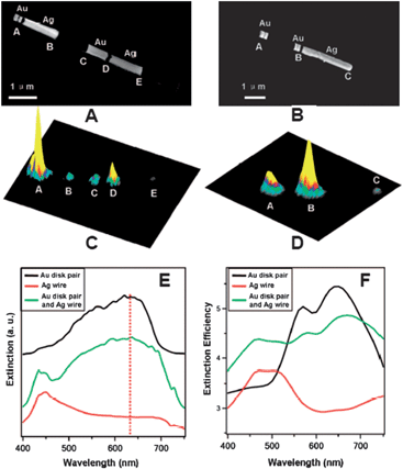 | ||
| Fig. 6 SEM images of multisegmented nanowires. (A) Left to right: a pair of Au nanodisks with a 30 nm gap and separated from a Ag segment by a 120 nm gap. The second set of nanostructures in the wire consists of a long Au segment separated by a 120 nm gap from a Ag segment. (B) Left to right: a pair of Au nanodisks with a 30 nm gap. The second set of nanostructures consists of a Au nanodisk pair separated from a long Ag segment. (C) and (D) are the corresponding 3D Raman images for the nanowires in (A) and (B). (E) Dark-field extinction spectra and (F) DDA simulation extinction efficiency of multisegmented nanowires. (Reprinted with permission from ref. 74, Wei et al., Nano Lett., 2008, 8, 3446; Copyright The American Chemical Society.) | ||
4.3 Periodic electromagnetic field enhancement along gold rods with nanogaps
It was demonstrated that by tailoring nanodisk sizes (120 nm thick, 360 nm diameter) and gap sizes (30 nm) in one-dimensional Au nanostructures, one could create Raman hot spots with maximum enhancement.60 However no significant Raman signal is obtained for a 10 nm gap within 3 μm long segments. OWL allows one for a systematic study of the variation of field enhancement in nanoscale gaps as a function of the length of the Au nanowire segments comprising the structures.82 The DDA method was used to calculate for the EF contribution at the 24 nm gap as a function of segment length (see Fig. 7A). The segment lengths were equally varied for both sides from 40 to 2000 nm in increments of 40 nm. The EF intensity oscillates periodically with the segment length every 560 nm without significant decay. Maxima occur at 120, 640, 1200, and 1760 nm when the wavelength of the incident light is 633 nm.54,83,84 The experimental results are in good agreement with the theoretical results (Fig. 7B), and demonstrate a 560 nm EF periodicity and relative maximum and minimum peak intensities obtained at the predicted segment lengths. These results allowed for a conceptual understanding of the physical phenomena involved in Raman scattering from small nanogaps in Au nanorod or nanowire structures. In addition, the results point to a way of optimizing gap size and segment length such that one can create structures that are large enough to be addressed electrically but have a SERS enhancement that is sufficient to provide useful spectroscopic data. | ||
| Fig. 7 (A) DDA simulation of the EF obtained at a 24 nm gap when varying symmetrically both segment lengths x. (B) Normalized SERS intensities measured at a 24 nm gap as a function of the rod segment length x. The curves show experimental results (o) and a comparison (dashed line) with theoretical calculations shown in (A). (C) MB SERS spectrum on a gapped Au rod. (Reprinted with permission from ref. 82, Pedano et al., Angew. Chem., Int. Ed., 2010, 49, 78; Copyright Wiley.) | ||
5. Plasmonic applications
Free-standing gap nanostructures can be fabricated by OWL with precise control over the compositional blocks and gap size, which can lead to tunable plasmonic properties with applications in various fields, such as biological sensing, analytical detection, and molecular electronics.5.1 Nanodisk codes for biological sensing
Due to the nature of the process, arrays of the optimum dimers were then pursued for novel applications in chemical and biological sensing and encoding.85 By controlling the relative distance between adjacent dimers in an array (Fig. 8), nanodisk codes (NDCs) were developed as a binary-reporting encoding scheme capable of high sensitivity, multimodal reporting, and detection. These structures represent a binary code where the presence of a dimer at a specific position represents a “1” and the absence represents a “0” in the physical readout. Upon preparation of these arrays and subsequent functionalization with a Raman chromophore of interest,27,86 the signal pattern of the binary code is easily observed using confocal Raman microscopy. As a proof of concept, the NDCs were utilized in the context of DNA sensing. NDCs were functionalized with different DNA sequences complementary to their respective target strands. Once functionalized, the solutions of NDCs were mixed together and subsequently added to a solution of DNA target strands and fluorophore-labeled DNA reporter strands. In this process, the code of the array as well as the presence of the dye produced a readout signal identified with Raman spectroscopy. The limit for target strand detection was down to 100 fM by using Au nanoparticles modified with the appropriate Raman-labelled DNA reporter strand (Fig. 8). Recently, the development of Ag NDCs has produced larger enhancements that led to an order of magnitude improvement in this limit of detection for DNA.67 By utilizing the large difference in signal intensity between Au and Ag at 532 nm excitation, a trinary encoding system was designed, where the larger signal from Ag disk pair adds an additional possibility to each digit location. Thus, the absence of a disk pair and the presence of a Au disk pair still equate to a “0” and a “1”, respectively, but Ag disk pairs, which exhibit a 3 orders of magnitude larger signal now become a “2”, greatly increasing the sophistication of the encoding system and the density of stored information.67 | ||
| Fig. 8 (A–C) FE-SEM images of 11111, 11011, and 10101-encoded NDCs, respectively. (D) Schematic representation of a three-strand DNA system. (E) Raman spectrum and (F) 3D scanning Raman images of DNA detection results at target concentrations of 50 pM, 5 pM, and control with no target (top to bottom, respectively). (Reprinted with permission from ref. 85, Qin et al., Nano Lett., 2007, 7, 3849; Copyright The American Chemical Society.) | ||
5.2 Analytical detection
An alternative DNA detection scheme was devised by combining the ability to electronically address the gapped Au nanowires (electrical trap) and the advantageous SERS enhancement of these structures. By applying an AC field to the nanogap device (Fig. 9A), the ionic DNA was concentrated within the gap where the strongest electrical filed gradient existed, and subsequently captured by the complementary DNA on the exposed SiO2 in the gap. Raman spectroscopy was able to detect an analyte signal for concentrations as low as 230 fM, over 20 times that of a comparable Raman detection system having no applied field and twice the reported sensitivity of tip-enhanced Raman spectroscopy87,88 (Fig. 9B). In principle, this OWL-based nanotrap method can be further improved by optimizing the electric field parameters, designing different nanogap structures/materials, or using nanoparticle-functionalized DNA probes for signal magnification. | ||
| Fig. 9 (A) An OWL-gap electrical device, with the trapped target molecules in the Raman hot spots. (B) An SEM image of a nanogap device in contact with electrodes and scanning Raman microscopy images showing that Raman intensities significantly increased owing to the accumulation of target DNA (at concentrations indicated) by an electric field into the nanogaps that function as Raman hot spots. (C) Schematic of the synthesis, device fabrication, surface functionalization, and measurement of hybrid PPy-rod/Au-rod/Au-disk pair nanostructures. (D) Schematic of telomerase binding and elongation on the Au nanostructure surface and current versus voltage plots of the AuPPy nanorod segment with binding of telomerase extracted from solutions of HeLa cells at different concentrations. (Reprinted with permission from ref. 89 and 90, Zheng et al., Angew. Chem., Int. Ed., 2008, 47, 1938 and Small, 2009, 5, 2537; Copyright Wiley.) | ||
A detection system containing both electrical and optical detection elements was constructed by OWL. PPy is a hole-carrying conducting polymer, and a Au/PPy interface behaves as a diode-like Schottky barrier. Binding events on the Au side of the wire can modulate the Au Fermi level, which is detectable by changes in conductance.91,92 Binding can also be measured with SERS by incorporating Au disk dimers at the end of the wire (Fig. 9C). The sensitivity of this electro-optic detection platform was demonstrated by testing for the presence of the cancer marker telomerase.90Telomerase is an enzyme that catalyzes the addition of the telomeric repeat sequence TTAGGG to the 3′-end of a DNA sequence in the presence of deoxyribonucleotide triphosphates (dNTPs).93–95 Following immobilization of the thiolated DNA recognition strand (5′ HS T5 AAT CCG TCG AGC AGA GTT 3′) on the Au segment of the OWL-generated Au/PPy wire, the devices were exposed to different concentrations of telomerase extracted from HeLa cells (1000, 5000, and 10![[thin space (1/6-em)]](https://www.rsc.org/images/entities/char_2009.gif) 000 cells) through a microfluidic channel (Fig. 9D). The binding of telomerase to the recognition strand was monitored by changes in conductance along the Au/PPy wire. The electrical portion of the device could detect the telomerase binding from as few as 1000 HeLa cells. In addition to the electrical detection of telomerase binding, the enzymatic activity could also be confirmed using SERS. Raman-labeled probes (5′ CCC TAA CCC TAA Cy5 3′) hybridize the DNA elongated by the telomerase, producing an enhanced Raman response within the gaps of the Au disk dimers. This system can be further optimized for greater sensitivity by using different surface receptors and sensor materials such as inorganic semiconductors, and may open up a host of new opportunities for studying many biological reactions in the life sciences.
000 cells) through a microfluidic channel (Fig. 9D). The binding of telomerase to the recognition strand was monitored by changes in conductance along the Au/PPy wire. The electrical portion of the device could detect the telomerase binding from as few as 1000 HeLa cells. In addition to the electrical detection of telomerase binding, the enzymatic activity could also be confirmed using SERS. Raman-labeled probes (5′ CCC TAA CCC TAA Cy5 3′) hybridize the DNA elongated by the telomerase, producing an enhanced Raman response within the gaps of the Au disk dimers. This system can be further optimized for greater sensitivity by using different surface receptors and sensor materials such as inorganic semiconductors, and may open up a host of new opportunities for studying many biological reactions in the life sciences.
5.3 Plasmonic spectroscopy to track the molecules in the nanogap for nanodevices
It has been shown that OWL can be used to rapidly construct electrodes with gaps small enough to accommodate “molecular wires”, and that the gap size can be tailored for a given molecule. The process has high-throughput, with respect to gap fabrication, and is extremely flexible with respect to the type of materials one can use as an electrode. The approach allows one to easily study the properties of molecular wires, and we have created an initial test-bed to identify unusual transport mechanism differences for a type of molecular wire as a function of temperature.96,97 Indeed, from a molecular electronics point of view, such OWL-fabricated structures offer a test-bed for molecular transport junctions (MTJs) formation with remarkable simplicity, stability, and scalability.Furthermore, a modular method for in situ synthesis of molecular wires to bridge nanogaps that allows spectroscopic tracking of the assembly process was demonstrated (Fig. 10). The click chemistry was used to demonstrate the in situ modular synthesis of molecular wires within the OWL-generated nanogaps. The copper(I)-catalyzed 1,3-dipolar Huisgen cycloaddition reaction (click reaction) between azide and alkyne groups was utilized to generate conducting molecular wires within OWL-fabricated nanogaps to form MTJs. An advantage of forming molecular wires using the click methodology within the OWL-generated nanogaps is that it is solution-processable. The use of click chemistry to form MTJs gives high yields and can be used to test different molecules, and the triazole form maintains conjugation in the molecular wires. In addition, this method overcomes a major challenge in the field of molecular electronics: the ability to spectroscopically track the assembly processes of MTJs within such tiny gaps. By using the azide–alkyne click reaction to affix molecules within the gap, the transport properties of different functional building blocks can be explored.
 | ||
| Fig. 10 (A) SEM image of an OWL-fabricated nanowire with a 100 nm nanogap, (B) 3D confocal scanning Raman images, and (C) Raman spectra taken of an OWL-fabricated gap structure. (Reprinted with permission from ref. 98, Chen et al., Angew. Chem., Int. Ed., 2009, 48, 5178; Copyright Wiley.) | ||
6. Conclusions and outlook
In summary, OWL is an emerging technique that has been used to fabricate free-standing 1D plasmonic nanostructures with precise control over the compositional blocks and to make gap structures as small as 2 nm. The ability of OWL to modulate the gap size over a wider range of 2 nm to 8 μm, especially in the context of gold or silver nanostructures, creates tunable plasmonic properties. Neither conventional lithography nor colloid particle assembly techniques are capable of routinely producing comparable structures over such size range. These free-standing 1D gapped nanostructures have not only shown coherent and unique phenomena in plasmonics, but also provided both theoretical and experimental validation. In addition, OWL allows one to produce unique heterostructures to probe plasmonic properties that are difficult to access using other fabrication methods. Plasmonic properties tuned by adjusting the gap size in the free-gapped nanostructure make them uniquely suitable for a wide range of applications in catalysis, biosensing, optics, and medical therapeutics. Additionally, these structures have potential for integration into nanoelectronics to develop active plasmonic devices for future ultrasmall and ultrafast devices and for any detection technique that relies on localized electric fields.Acknowledgements
XC thanks the support from A*STAR through SERC-TSRP (10215200135) and the National Research Foundation of Singapore (NRF-RF2009-04 and CREATE). SL thanks the support from Singapore MOE (Tier 1).Notes and references
- G. C. Schatz and T. W. Odom, Chem. Rev., 2011, 111, 3667–3668 Search PubMed.
- N. J. Halas, Nano Lett., 2010, 10, 3816–3822 CrossRef CAS.
- W. L. Barnes, A. Dereux and T. W. Ebbesen, Nature, 2003, 424, 824–830 CrossRef CAS.
- V. Giannini, A. I. Fernandez-Dominguez, S. C. Heck and S. A. Maier, Chem. Rev., 2011, 111, 3888–3912 Search PubMed.
- M. W. Knight, H. Sobhani, P. Nordlander and N. J. Halas, Science, 2011, 332, 702–704 CrossRef CAS.
- C. A. Mirkin, R. L. Letsinger, R. C. Mucic and J. J. Storhoff, Nature, 1996, 382, 607–609 CrossRef CAS.
- J. J. Du, Y. H. Sun, L. Jiang, X. B. Cao, D. P. Qi, S. Y. Yin, J. Ma, F. Y. C. Boey and X. D. Chen, Small, 2011, 7, 1407–1411 Search PubMed.
- J. N. Anker, W. P. Hall, O. Lyandres, N. C. Shah, J. Zhao and R. P. Van Duyne, Nat. Mater., 2008, 7, 442–453 CrossRef CAS.
- C. Ungureanu, R. Kroes, W. Petersen, T. A. M. Groothuis, F. Ungureanu, H. Janssen, F. W. B. van Leeuwen, R. P. H. Kooyman, S. Manohar and T. G. van Leeuwen, Nano Lett., 2011, 11, 1887–1894 Search PubMed.
- E. Ozbay, Science, 2006, 311, 189–193 CrossRef CAS.
- A. S. K. Hashmi and G. J. Hutchings, Angew. Chem., Int. Ed., 2006, 45, 7896–7936 CrossRef.
- S. Eustis and M. A. El-Sayed, Chem. Soc. Rev., 2006, 35, 209–217 RSC.
- J. R. Cole and N. J. Halas, Appl. Phys. Lett., 2006, 89, 153120 CrossRef.
- A. Aubry, D. Y. Lei, A. I. Fernandez-Dominguez, Y. Sonnefraud, S. A. Maier and J. B. Pendry, Nano Lett., 2010, 10, 2574–2579 CrossRef CAS.
- P. Banerjee, D. Conklin, S. Nanayakkara, T. H. Park, M. J. Therien and D. A. Bonnell, ACS Nano, 2010, 4, 1019–1025 CrossRef CAS.
- S. A. Maier, Plamonics: Fundamentals and Applicants, Springer, New York, 2007 Search PubMed.
- C. Burda, X. B. Chen, R. Narayanan and M. A. El-Sayed, Chem. Rev., 2005, 105, 1025–1102 CrossRef CAS.
- M. Grzelczak, J. Perez-Juste, P. Mulvaney and L. M. Liz-Marzan, Chem. Soc. Rev., 2008, 37, 1783–1791 RSC.
- N. J. Halas, S. Lal, W. S. Chang, S. Link and P. Nordlander, Chem. Rev., 2011, 111, 3913–3961 CrossRef CAS.
- M. Rycenga, C. M. Cobley, J. Zeng, W. Y. Li, C. H. Moran, Q. Zhang, D. Qin and Y. N. Xia, Chem. Rev., 2011, 111, 3669–3712 CrossRef CAS.
- T. Atay, J. H. Song and A. V. Nurmikko, Nano Lett., 2004, 4, 1627–1631 CrossRef CAS.
- K. Kneipp, H. Kneipp and J. Kneipp, Acc. Chem. Res., 2006, 39, 443–450 CrossRef CAS.
- S. Y. Lee, L. Hung, G. S. Lang, J. E. Cornett, I. D. Mayergoyz and O. Rabin, ACS Nano, 2010, 4, 5763–5772 CrossRef CAS.
- L. Jiang, Y. H. Sun, C. Nowak, A. Kibrom, C. J. Zou, J. Ma, H. Fuchs, S. Z. Li, L. F. Chi and X. D. Chen, ACS Nano, 2011, 5, 8288–8294 Search PubMed.
- S. M. Nie and S. R. Emery, Science, 1997, 275, 1102–1106 CrossRef CAS.
- H. Ko, S. Singamaneni and V. V. Tsukruk, Small, 2008, 4, 1576–1599 CrossRef CAS.
- D. P. Fromm, A. Sundaramurthy, P. J. Schuck, G. Kino and W. E. Moerner, Nano Lett., 2004, 4, 957–961 CrossRef CAS.
- W. Kubo and S. Fujikawa, Nano Lett., 2011, 11, 8–15 Search PubMed.
- P. K. Jain, W. Y. Huang and M. A. El-Sayed, Nano Lett., 2007, 7, 2080–2088 CrossRef CAS.
- Z. Y. Tang and N. A. Kotov, Adv. Mater., 2005, 17, 951–962 CrossRef CAS.
- S. Lin, M. Li, E. Dujardin, C. Girard and S. Mann, Adv. Mater., 2005, 17, 2553–2559 CrossRef CAS.
- W. H. Binder, Angew. Chem., Int. Ed., 2005, 44, 5172–5175 CrossRef CAS.
- H. W. Duan, D. Y. Wang, D. G. Kurth and H. Mohwald, Angew. Chem., Int. Ed., 2004, 43, 5639–5642 CrossRef CAS.
- J. Liao, L. Bernard, M. Langer, C. Schonenberger and M. Calame, Adv. Mater., 2006, 18, 2444–2447 CrossRef CAS.
- Y. Yang, J. L. Shi, T. Tanaka and M. Nogami, Langmuir, 2007, 23, 12042–12047 CrossRef CAS.
- W. L. Cheng, M. J. Campolongo, J. J. Cha, S. J. Tan, C. C. Umbach, D. A. Muller and D. Luo, Nat. Mater., 2009, 8, 519–525 CrossRef CAS.
- L. Jiang, W. C. Wang, H. Fuchs and L. F. Chi, Small, 2009, 5, 2819–2822 CrossRef CAS.
- R. C. Mucic, J. J. Storhoff, C. A. Mirkin and R. L. Letsinger, J. Am. Chem. Soc., 1998, 120, 12674–12675 CrossRef CAS.
- W. Y. Li, P. H. C. Camargo, X. M. Lu and Y. N. Xia, Nano Lett., 2009, 9, 485–490 CrossRef CAS.
- D. K. Lim, K. S. Jeon, J. H. Hwang, H. Kim, S. Kwon, Y. D. Suh and J. M. Nam, Nat. Nanotechnol., 2011, 6, 452–460 Search PubMed.
- B. Kim, S. L. Tripp and A. Wei, J. Am. Chem. Soc., 2001, 123, 7955–7956 CrossRef CAS.
- L. D. Qin, S. Park, L. Huang and C. A. Mirkin, Science, 2005, 309, 113–115 CrossRef.
- M. J. Banholzer, L. D. Qin, J. E. Millstone, K. D. Osberg and C. A. Mirkin, Nat. Protoc., 2009, 4, 838–848 Search PubMed.
- B. T. Draine and P. J. Flatau, J. Opt. Soc. Am. A, 1994, 11, 1491–1499 CrossRef.
- J. Zhao, A. O. Pinchuk, J. M. McMahon, S. Z. Li, L. K. Ausman, A. L. Atkinson and G. C. Schatz, Acc. Chem. Res., 2008, 41, 1710–1720 CrossRef CAS.
- J. Zhang, S. Z. Li, J. S. Wu, G. C. Schatz and C. A. Mirkin, Angew. Chem., Int. Ed., 2009, 48, 7787–7791 CrossRef CAS.
- M. N'Gom, S. Z. Li, G. Schatz, R. Erni, A. Agarwal, N. Kotov and T. B. Norris, Phys. Rev. B: Condens. Matter Mater. Phys., 2009, 80, 113411 CrossRef.
- M. Kerker, D. S. Wang and H. Chew, Appl. Opt., 1980, 19, 4159–4174 CrossRef CAS.
- S. J. Hurst, E. K. Payne, L. D. Qin and C. A. Mirkin, Angew. Chem., Int. Ed., 2006, 45, 2672–2692 CrossRef CAS.
- C. R. Martin, Science, 1994, 266, 1961–1966 CrossRef CAS.
- C. K. Preston and M. Moskovits, J. Phys. Chem., 1993, 97, 8495–8503 CrossRef CAS.
- D. Almawlawi, C. Z. Liu and M. Moskovits, J. Mater. Res., 1994, 9, 1014–1018 CrossRef CAS.
- H. Masuda and K. Fukuda, Science, 1995, 268, 1466–1468 CrossRef CAS.
- E. K. Payne, K. L. Shuford, S. Park, G. C. Schatz and C. A. Mirkin, J. Phys. Chem. B, 2006, 110, 2150–2154 CrossRef CAS.
- S. Kim, K. L. Shuford, H. M. Bok, S. K. Kim and S. Park, Nano Lett., 2008, 8, 800–804 CrossRef CAS.
- L. D. Qin, J. W. Jang, L. Huang and C. A. Mirkin, Small, 2007, 3, 86–90 CrossRef CAS.
- K. D. Osberg, A. L. Schmucker, A. J. Senesi and C. A. Mirkin, Nano Lett., 2011, 11, 820–824 Search PubMed.
- C. Liusman, S. Z. Li, X. D. Chen, W. Wei, H. Zhang, G. C. Schatz, F. Boey and C. A. Mirkin, ACS Nano, 2010, 4, 7676–7682 CrossRef CAS.
- X. D. Chen, S. Z. Li, C. Xue, M. J. Banholzer, G. C. Schatz and C. A. Mirkin, ACS Nano, 2009, 3, 87–92 CrossRef CAS.
- L. D. Qin, S. L. Zou, C. Xue, A. Atkinson, G. C. Schatz and C. A. Mirkin, Proc. Natl. Acad. Sci. U. S. A., 2006, 103, 13300–13303 CrossRef CAS.
- E. Hao and G. C. Schatz, J. Chem. Phys., 2004, 120, 357–366 CrossRef CAS.
- K. L. Kelly, E. Coronado, L. L. Zhao and G. C. Schatz, J. Phys. Chem. B, 2003, 107, 668–677 CrossRef CAS.
- S. Z. Li, M. L. Pedano, S. H. Chang, C. A. Mirkin and G. C. Schatz, Nano Lett., 2010, 10, 1722–1727 CrossRef CAS.
- M. J. Banholzer, S. Z. Li, J. B. Ketter, D. I. Rozkiewicz, G. C. Schatz and C. A. Mirkin, J. Phys. Chem. C, 2008, 112, 15729–15734 CrossRef CAS.
- J. Dorfmuller, R. Vogelgesang, R. T. Weitz, C. Rockstuhl, C. Etrich, T. Pertsch, F. Lederer and K. Kern, Nano Lett., 2009, 9, 2372–2377 CrossRef.
- G. Laurent, N. Felidj, J. Aubard, G. Levi, J. R. Krenn, A. Hohenau, G. Schider, A. Leitner and F. R. Aussenegg, J. Chem. Phys., 2005, 122, 011102 Search PubMed.
- M. J. Banholzer, K. D. Osberg, S. Z. Li, B. F. Mangelson, G. C. Schatz and C. A. Mirkin, ACS Nano, 2010, 4, 5446–5452 CrossRef CAS.
- D. Graham and K. Faulds, Chem. Soc. Rev., 2008, 37, 1042–1051 RSC.
- C. D. Keating, K. M. Kovaleski and M. J. Natan, J. Phys. Chem. B, 1998, 102, 9404–9413 CrossRef CAS.
- J. Jiang, K. Bosnick, M. Maillard and L. Brus, J. Phys. Chem. B, 2003, 107, 9964–9972 CrossRef CAS.
- M. Moskovits, Rev. Mod. Phys., 1985, 57, 783–826 CrossRef CAS.
- G. L. Hornyak, C. J. Patrissi and C. R. Martin, Nanostruct. Mater., 1997, 9, 705–708 CrossRef CAS.
- W. Wei, S. Z. Li, J. E. Millstone, M. J. Banholzer, X. D. Chen, X. Y. Xu, G. C. Schatz and C. A. Mirkin, Angew. Chem., Int. Ed., 2009, 48, 4210–4212 CrossRef CAS.
- W. Wei, S. Z. Li, L. D. Qin, C. Xue, J. E. Millstone, X. Y. Xu, G. C. Schatz and C. A. Mirkin, Nano Lett., 2008, 8, 3446–3449 CrossRef CAS.
- J. Lehmann, M. Merschdorf, W. Pfeiffer, A. Thon, S. Voll and G. Gerber, Phys. Rev. Lett., 2000, 85, 2921–2924 Search PubMed.
- C. Kennerknecht, H. Hovel, M. Merschdorf, S. Voll and W. Pfeiffer, Appl. Phys. B: Lasers Opt., 2001, 73, 425–429 Search PubMed.
- H. Y. Lin and Y. F. Chen, Appl. Phys. Lett., 2006, 88, 101914 Search PubMed.
- Y. Sakata, K. Domen, K. Maruya and T. Onishi, Catal. Lett., 1990, 4, 169–172 CrossRef.
- L. A. Bauer, D. H. Reich and G. J. Meyer, Langmuir, 2003, 19, 7043–7048 CrossRef CAS.
- A. K. Salem, P. C. Searson and K. W. Leong, Nat. Mater., 2003, 2, 668–671 CrossRef CAS.
- B. Ren, G. K. Liu, X. B. Lian, Z. L. Yang and Z. Q. Tian, Anal. Bioanal. Chem., 2007, 388, 29–45 CrossRef CAS.
- M. L. Pedano, S. Z. Li, G. C. Schatz and C. A. Mirkin, Angew. Chem., Int. Ed., 2010, 49, 78–82 Search PubMed.
- E. S. Barnard, J. S. White, A. Chandran and M. L. Brongersma, Opt. Express, 2008, 16, 16529–16537 Search PubMed.
- C. A. Pfeiffer, E. N. Economou and K. L. Ngai, Phys. Rev. B: Solid State, 1974, 10, 3038–3051 Search PubMed.
- L. Qin, M. J. Banholzer, J. E. Millstone and C. A. Mirkin, Nano Lett., 2007, 7, 3849–3853 CrossRef CAS.
- H. Wang, C. S. Levin and N. J. Halas, J. Am. Chem. Soc., 2005, 127, 14992–14993 CrossRef CAS.
- J. A. Dieringer, A. D. McFarland, N. C. Shah, D. A. Stuart, A. V. Whitney, C. R. Yonzon, M. A. Young, X. Y. Zhang and R. P. Van Duyne, Faraday Discuss., 2006, 132, 9–26 RSC.
- B. Pettinger, G. Picardi, R. Schuster and G. Ertl, Single Mol., 2002, 3, 285–294 CrossRef CAS.
- G. F. Zheng, L. D. Qin and C. A. Mirkin, Angew. Chem., Int. Ed., 2008, 47, 1938–1941 Search PubMed.
- G. F. Zheng, X. D. Chen and C. A. Mirkin, Small, 2009, 5, 2537–2540 Search PubMed.
- P. R. Somani and S. Radhakrishnan, Chem. Phys. Lett., 2003, 379, 401–405 Search PubMed.
- F. Hache, D. Ricard, C. Flytzanis and U. Kreibig, Appl. Phys. A: Solids Surf., 1988, 47, 347–357 CrossRef.
- N. W. Kim, M. A. Piatyszek, K. R. Prowse, C. B. Harley, M. D. West, P. L. C. Ho, G. M. Coviello, W. E. Wright, S. L. Weinrich and J. W. Shay, Science, 1994, 266, 2011–2015 CrossRef CAS.
- G. B. Morin, Cell, 1989, 59, 521–529 CrossRef CAS.
- Y. Weizmann, F. Patolsky, O. Lioubashevski and I. Willner, J. Am. Chem. Soc., 2004, 126, 1073–1080 CrossRef CAS.
- X. D. Chen, Y. M. Jeon, J. W. Jang, L. Qin, F. W. Huo, W. Wei and C. A. Mirkin, J. Am. Chem. Soc., 2008, 130, 8166–8168 CrossRef CAS.
- X. D. Chen, S. Yeganeh, L. D. Qin, S. Z. Li, C. Xue, A. B. Braunschweig, G. C. Schatz, M. A. Ratner and C. A. Mirkin, Nano Lett., 2009, 9, 3974–3979 CrossRef CAS.
- X. D. Chen, A. B. Braunschweig, M. J. Wiester, S. Yeganeh, M. A. Ratner and C. A. Mirkin, Angew. Chem., Int. Ed., 2009, 48, 5178–5181 CrossRef CAS.
| This journal is © The Royal Society of Chemistry 2012 |