Nanorainforest solar cells based on multi-junction hierarchical p-Si/n-CdS/n-ZnO nanoheterostructures†
Wei
Wang
a,
Qing
Zhao
*a,
Kevin
Laurent
a,
Y.
Leprince-Wang
b,
Zhi-Min
Liao
a and
Dapeng
Yu
*a
aState Key Laboratory for Mesoscopic Physics and Electron Microscopy Laboratory, School of Physics, Peking University, Beijing, 100871, P. R. China. E-mail: zhaoqing@pku.edu.cn; yudp@pku.edu.cn
bUniversite Paris-Est, LPMDI, CNRS FRE3300, 5 bd Descartes, F-77454, Marne La Vallee cedex 2, France
First published on 11th November 2011
Abstract
Solar cells based on one-dimensional nanostructures have recently emerged as one of the most promising candidates to achieve high-efficiency solar energy conversion due to their reduced optical reflection, enhanced light absorption, and enhanced carrier collection. In nature, the rainforest, consisting of several stereo layers of vegetation, is the highest solar-energy-using ecosystem. Herein, we gave an imitation of the rainforest configuration in nanostructure-based solar cell design. Novel multi-layer nanorainforest solar cells based on p-Si nanopillar array/n-CdS nanoparticles/n-ZnO nanowire array heterostructures were achieved via a highly accessible, reproducible and controllable fabrication process. By choosing materials with appropriate bandgaps, an efficient light absorption and enhanced light harvesting were achieved due to the wide range of the solar spectrum covered. Si nanopillar arrays were introduced as direct conduction pathways for photon-generated charges’ efficient collection and transport. The unique strategy using PMMA as a void-filling material to obtain a continuous, uniform and low resistance front electrode has significantly improved the overall light conversion efficiency by two orders of magnitude. These results demonstrate that nanorainforest solar cells, along with wafer-scale, low-cost and easily controlled processing, open up substantial opportunities for nanostructure photovoltaic devices.
1. Introduction
One-dimensional (1D) nanostructures have recently emerged as one of the most promising candidates for high-efficiency solar cells due to their reduced optical reflection, enhanced carrier collection, and higher surface area for light harvesting compared to planar structures.1–8 The choice of material system in nanowire-based solar cell structures is particularly important. In particular, ZnO nanowires have been studied intensively as a promising material for photovoltaic devices due to their wide band gap (3.37 eV), large exciton binding energy (60 meV), and high photoconductivity gain.9Si nanopillars have attracted considerable attention for energy harvesting applications due to their unique optical and electrical properties.10 Photodiodes based on p-Si nanowire/n-ZnO film and p-Si/n-ZnO radial heterojunction nanowires have been recently reported, but the obtained conversion efficiency is not satisfying because of their poor ZnO crystalline quality, the challenge in growing ZnO/Si hierarchical nanoheterostructures and poor contact at junctions.11–13 Very recently, a ZnO/Si hierarchical nanoheterostructure photodetector was reported by solution synthesis.14 However, it still suffers from low energy conversion because of insufficient light utilization in the visible region due to the single junction of the ZnO/Si heterostructures and recombination loss via defects. In this regard, multi-layer solar cells composed of several layers with different band gaps are highly desirable to cover a wide range of the solar spectrum in order to increase the overall efficiency of solar energy conversion. For instance, CdS has a direct band gap of 2.4 eV, which is optimal between ZnO (3.37 eV) and Si (1.12 eV), making it attractive in solar cell applications.15,16 Multi-junction solar cells based on hierarchical Si/CdS/ZnO nanoheterostructures remain unreported up to date.In multi-layer planar solar cells based on thin films, current matching is a key issue since the current produced by the solar cell is dominated by the layer which produces the least amount of current.17 The photocurrent generated in each layer should be almost the same in order to maximize the current output.17 A direct pathway along 1D crystalline nanostructures would diminish the possibility of charge recombination and rapidly collect photogenerated electrons.18 Introducing sufficiently long 1D nanostructures in the multi-layer design might solve the current-matching problem, since they could provide significant enhancement of the junction area with reduced minority carrier collection length.
On the other hand, fabrication of a high light transmission and low resistance front electrode of nanostructured solar cells is still a challenging issue. The device performance was found to be severely affected due to poor top-contact.19,20 Direct deposition of a transparent conductive layer (metal film or indium tin oxides (ITO) layer) on the surface of the nanowires always makes the top-contact high in resistivity.14,21–23 Liquid top electrodes allow a full contact with the nanowires but give low charge mobility and make cell packaging difficult.24,25 Novel methods to develop uniform, good top-contact with low resistance are highly desirable for achieving high-efficiency nanowire based solar cells.
In nature, the rainforest, consisting of several stereo layers of vegetation (Fig. 1(a)), is the highest solar-energy-using ecosystem. Herein, we gave an imitation of the rainforest configuration in nanoheterostructure-based solar cell design (Fig. 1(b)). A nanorainforest solar cell based on a multi-layer nanoheterostructure (p-Si nanopillar arrays/n-CdS nanoparticles/n-ZnO nanowire arrays) was fabricated to use solar energy efficiently, like the rainforest (Fig. 1(c)). Si nanopillar arrays through all layers were introduced as trunks, behaving as direct conduction pathway to collect photogenerated carriers and reduce charge recombination. PMMA was creatively employed in providing a continuous and uniform flat surface to help the formation of a high quality uniform top contact, which led to a two orders of magnitude solar cell efficiency increase. Furthermore, each step of the solar cell fabrication can be precisely controlled and the method is low-cost and easy for large scale production.
 | ||
| Fig. 1 (a) Schematic sketch of rainforest vegetation. (b) Designed nanorainforest solar cell structure in order to efficiently use sunlight. (c) Typical cross-section SEM image of the fabricated nanorainforest solar cells based on p-Si/n-CdS/n-ZnO nanoheterostructures. | ||
2. Experimental
A schematic diagram of the fabrication process was illustrated in Fig. 2. Briefly, a close-packed hexagonal monolayer of polystyrene (PS) nanospheres was first prepared on p-type Si wafer surface (Fig. 2(a)) according to a self-assembly technique at the air/liquid interface reported by Liu et al.26 The size of the PS nanospheres has been reduced via a plasma etching technique to get an optimal filling ratio. The size of the PS nanospheres could be finely tuned via different plasma etching times. After plasma etching, a thin silver layer (50 nm) was sputtered onto Si surface to form a periodic nanohole catalyst template (Fig. 2(b)). Si nanopillar arrays were obtained by immersing the silver pattern Si wafer in an oxidizing HF solution (Fig. 2(c)), following the method developed by Peng et al.27,28 The diameter and length of our Si nanopillars can be well controlled by the PS nanosphere size, and the chemical etching time, respectively. Then a CdS nanoparticle layer was deposited onto the Si nanopillars via a simple chemical bath deposition method (Fig. 2(d)).29 Subsequently, ZnO nanowires arrays with a ZnO thin layer were grown on this structure by the chemical vapor deposition method (Fig. 2e) and the thickness of ZnO layer could be controlled by changing the growth condition.30ZnO layer was doped with Al in order to increase the carrier density. For the front electrode fabrication, PMMA was firstly spin coated onto ZnO nanowires (Fig. 2(f)), then the PMMA was plasma etched to let ∼150 nm ZnO nanowire tips stand out from the PMMA surface (Fig. 2(g)). A ∼150 nm ITO film was subsequently sputtered onto the ZnO nanowire tips to make an Ohmic contact with the ZnO nanowires (Fig. 2(h)). The thickness was set to ∼150 nm in order to balance the light transmission and resistivity of ITO film.31 | ||
| Fig. 2 Schematic diagram of the solar cell fabrication process. (a) A wafer-scale close-packed hexagonal PS nanospheres monolayer on hydrophilic p-Si wafer surface is prepared. (b) Plasma etching of the PS nanospheres reduces the size and obtains the required filling ratio. Sputtering of a thin silver layer onto an Si surface with reduced size PS nanospheres forms a periodic nanohole catalyst template. (c) Si nanopillar arrays are obtained by wet chemical etching. (d) A CdS nanoparticle layer is deposited onto the Si nanopillars. (e) ZnO nanowires arrays are deposited with a ZnO layer grown via a CVD method. (f) Spin coating of PMMA onto ZnO nanowires. (g) Plasma etching of PMMA allows the ZnO nanowires stand out from the surface of PMMA. (h) Deposition of an ITO film onto the surface of ZnO nanowires forms an Ohmic contact with the ZnO nanowires. | ||
2.1 Si nanopillar array fabrication
Si nanopillar arrays were obtained via a metal-assisted chemical etching method.23,26,28 In detail, a (100) Si wafer (p-type, 2–4 Ωcm) was first made hydrophilic in boiling piranha solution (4![[thin space (1/6-em)]](https://www.rsc.org/images/entities/char_2009.gif) :1 (v/v) H2SO4–H2O2) and RCA solution (1:1:5 (v/v/v) NH3·H2O–H2O2–H2O), each for 1 h. A 10% aqueous PS spheres suspension, as purchased (d = 762 nm, Micro-particles GmbH Corp, Germany), was diluted by an equal volume of ethanol, and then was slowly applied to the surface of deionized water in a glass culture dish. After the close-packed hexagonal PS spheres monolayer formed on the water surface, a drop of lauryl sodium sulfate solution was added to the base water to consolidate the mask into a stable film. Subsequently, the PS spheres mask was transferred onto the hydrophilic surface of p-Si wafer by slow water drainage. The PS spheres monolayer was then annealed at 110 °C for 30 min to ensure full adherence to the Si surface. The size of the PS spheres was then reduced to 500 nm using plasma etching (10 sccm air flow rate, 10 Pa pressure, and 50 W applied power with Femto, Diener Electronic, Germany). A thin silver layer (50 nm) was sputtered onto an Si surface to form a periodic nanohole catalyst template after the plasma etching process. The Si nanopillar arrays were obtained by immersing the silver patterned Si wafer in an oxidizing HF solution (32 ml Milli-Q water, 4 ml HF, 4 g NH4F and 2 ml H2O2) at 40 °C in a water bath. After etching, the Si wafer was immersed in boiling nitric acid solution (1:1 (v/v) HNO3–H2O) for 30 min to remove the PS spheres and the silver film. The Si nanopillar arrays was annealed at 900 °C under O2 for 2 h and immersed in a 5% HF solution to remove amorphous silicon on the nanopillar surface. This step can lead to a very good contact between the Si nanopillars and ZnO.
:1 (v/v) H2SO4–H2O2) and RCA solution (1:1:5 (v/v/v) NH3·H2O–H2O2–H2O), each for 1 h. A 10% aqueous PS spheres suspension, as purchased (d = 762 nm, Micro-particles GmbH Corp, Germany), was diluted by an equal volume of ethanol, and then was slowly applied to the surface of deionized water in a glass culture dish. After the close-packed hexagonal PS spheres monolayer formed on the water surface, a drop of lauryl sodium sulfate solution was added to the base water to consolidate the mask into a stable film. Subsequently, the PS spheres mask was transferred onto the hydrophilic surface of p-Si wafer by slow water drainage. The PS spheres monolayer was then annealed at 110 °C for 30 min to ensure full adherence to the Si surface. The size of the PS spheres was then reduced to 500 nm using plasma etching (10 sccm air flow rate, 10 Pa pressure, and 50 W applied power with Femto, Diener Electronic, Germany). A thin silver layer (50 nm) was sputtered onto an Si surface to form a periodic nanohole catalyst template after the plasma etching process. The Si nanopillar arrays were obtained by immersing the silver patterned Si wafer in an oxidizing HF solution (32 ml Milli-Q water, 4 ml HF, 4 g NH4F and 2 ml H2O2) at 40 °C in a water bath. After etching, the Si wafer was immersed in boiling nitric acid solution (1:1 (v/v) HNO3–H2O) for 30 min to remove the PS spheres and the silver film. The Si nanopillar arrays was annealed at 900 °C under O2 for 2 h and immersed in a 5% HF solution to remove amorphous silicon on the nanopillar surface. This step can lead to a very good contact between the Si nanopillars and ZnO.
2.2 CdS layer deposition
The Si nanopillars were immersed in solution (9.86 g Cd(Ac)2 dissolved in 170 ml of Milli-Q water, 20 ml NH3·H2O, 10 ml triethylamine (TEA) and 5.36 g thiourea) and heated for 30 min at 80 °C.2.3 ZnO nanowire array growth
A mixture of 0.2 g Zn powder and 0.05 g AlCl3 powder in a quartz tube and Si wafer 2 cm downstream away from the quartz tube were placed in a furnace tube. Then the furnace was heated to and maintained at 700 °C, 10 Pa for 5 min with 100 sccm Ar and 8 sccm O2, larger O2 flux leading to a thicker ZnO film.2.4 Top front electrode fabrication
A drop of PMMA (8%) mixed with anisole was spin coated (1000 rpm, 2 min) onto the top of ZnO nanowires. After evaporation of the solvent, air plasma etching process (flow rate: 15 sccm, pressure: 10 Pa, power: 50 W for 30 s) was used to allow 150 nm ZnO nanowires standing out from PMMA layer. The solar cell was completed by sputtering a 150 nm ITO film onto ZnO nanowires to make the ITO have direct contact with the ZnO nanowires.2.5 Characterization, current density-voltage and sheet resistivity measurement
All morphology was characterized by scanning electron microscopy (SEM, FEI, NanoSEM 430). The spectral photoresponse and optical properties were measured by QTest Station 1000AD system (CrownTech Inc). The current density–voltage (J–V) characteristics were tested by a Keithley 4200SCS (Keithley Instruments, Inc). J–V curves were obtained in the dark and under 1.5 a.m. solar simulator illumination (100 mW cm−2, IVTest Station 2000 (CrownTech. INC)). The solar simulator was carefully calibrated before each measurement. More than 20 solar cell devices were tested and the average active area of the cell is 1 cm2. The sheet resistivity of front electrodes were measured by a four-probe probe station (Keithley 4200SCS) by the collinear four-probe method. In detail, the four-probe probe station was shield in a steel box, to avoid electrostatic and light interference. The voltage between two inner probes were measured under the applied bias current on two outer probes of 10 mA, 1 mA, 1 mA for ZnO/PMMA/ITO, ZnO/ITO, ZnO front electrode type, respectively. Then the applied bias current was reversed to measure another inner voltage. The resistivity was calculated by averaging the resistivity under the forward and reverse bias current. The distance between each two probes was 1 mm.3. Results and discussion
Fig. 3 provides typical morphology of the fabricated solar cells in steps. Fig. 3(a) is the SEM image showing PS nanospheres with diameter of 762 nm prepared on Si wafer in a regular pattern. The diameter of the PS spheres was reduced to 500 nm by varying the duration of plasma etching (Fig. 3(b)). Fig. 3(c) shows the top view and side view (as inset) SEM images of the Si nanopillar arrays (d ∼ 500 nm, l ∼5 μm). The nanopillar array diameter and length were used to tailor the absorption spectrum of the nanopillar solar cell.32,33 It was reported that the solar energy conversion efficiency could reach a maximum when the Si nanopillar array periodicity is around 500 nm with a 0.5 filling ratio.32Si nanopillar arrays of several microns (∼5 μm) in length have been noted for their strong broadband optical absorption.33 Note that such long Si nanopillars could penetrate the entire nanorainforest solar cell multi-layer architecture, and act as direct conduction pathway for photogenerated carriers. Accordingly we adjusted the diameter and length of Si nanopillar arrays to get the optimum efficiency. The diameter and filling ratio of PS nanospheres and Si nanopillars can be fully tuned via our controllable method. SEM images of PS nanospheres and Si nanopillar arrays with different sizes and filling ratios are shown in Fig. 4 and Fig. 5, respectively. Top view and cross section SEM images in Fig. 3(d) clearly show CdS nanoparticle layer deposition onto Si nanopillar arrays. More SEM, TEM and EDS analyses of CdS nanoparticles can be found in Fig. S3 and S4 in the ESI.† The highly oriented ZnO nanowire arrays (d = 250 nm, l = 850 nm) with a ∼600 nm ZnO layer were grown on the deposited CdS layer (Fig. 3(e)). The inset of Fig. 3(e) demonstrates the uniformity and high orientation of the as-grown ZnO nanowire arrays. Energy dispersive spectra (EDS) of the three layers are shown in Fig. S1 in the ESI.† The thickness of ZnO layers could be tuned via experimental parameters and further optical study shows thickness-dependent light transmission properties, suggesting that the controlled fabrication process can get optimum light absorption from the ZnO layer. Cross section SEM images of ZnO layers with different thickness are shown in Fig. S2 in the ESI.† | ||
| Fig. 3 (a) Top view SEM image of close-packed hexagonal PS nanospheres monolayer on a hydrophilic p-Si wafer surface. (b) Top view SEM image of PS nanospheres monolayer after air plasma etching with a filling ratio of 50%. (c) Top view SEM image of the obtained Si nanopillar arrays. Inset: cross section SEM image. (d) Top view SEM image of CdS nanocrystal deposited onto the Si nanopillars’ surface. Inset: cross section SEM image. (e) Cross section SEM image of ZnO film and ZnO nanowire arrays grown on the Si nanopillars and CdS layer. Inset: top view SEM image. (f) Cross section SEM image of PMMA spin coating onto ZnO nanowires. Inset: Top view SEM image. (g) Cross section SEM image of ∼150 nm ZnO nanowire tips standing out from PMMA surface after plasma etching PMMA. Inset: Top view SEM image. (h) Cross section SEM image of an ITO layer covering the surface of the exposed ZnO nanowires to form a very good contact with the ZnO nanowires. Inset: Top view SEM image. (i) Cross section SEM image of the completed solar cells. | ||
 | ||
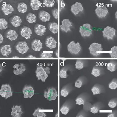
| Fig. 4 Top view SEM images of PS nanospheres monolayer with different sizes and filling ratio. (a) 650 nm, 85.5%. (b) 550 nm, 72.4%. (c) 440 nm, 57.9%. (d) 280 nm, 36.8%. Scale bar: 500 nm. | ||
 | ||
| Fig. 5 Top view SEM images of Si nanopillar arrays with different filling ratio. (a) 65.8%. (b) 55.9%. (c) 52.6%. (d) 26.3%. Scale bar: 500 nm. | ||
Fig. 3(f) and its inset reveal a flat and continuous surface after PMMA coating onto the ZnO nanowire arrays. Fig. 3(g) and its inset clearly show that the ∼150 nm ZnO nanowire tips stood out from the PMMA surface after plasma etching the PMMA. After ITO coating on the surface of the PMMA film and ZnO nanowires, ITO has made a very good contact with the ZnO nanowires due to the help of the PMMA underneath, as shown in Fig. 3(h). Finally, the nanorainforest solar cell based on multi-layer p-Si/n-CdS/n-ZnO nanoheterostructures was fabricated; see the typical cross section SEM image in Fig. 3(i). It should be pointed out that there is a plasma etching PMMA process (Fig. 3(g)), by which way the ZnO nanowire tips could be made contact directly with ITO after ITO sputtering (Fig. 3(h)). PMMA is very important in this strategy, because it provides a flat and continuous surface for further conductive ITO layer deposition. The contact between ITO and ZnO nanowires has been significantly improved with PMMA as the supporting membrane underneath, which is more advantageous than direct deposition of ITO onto ZnO nanowires without using PMMA. To further emphasize the significant function of PMMA in achieving a good top-contact, top-contact without using PMMA was made by directly sputtering ITO on ZnO nanowires; see the SEM images in Fig. 6. Since the ZnO nanowires surface is not flat, the contact is not continuous in this case and results in a very high resistivity, almost two orders of magnitude higher than the ZnO/PMMA/ITO top contact. The detailed data will be discussed later in Table 1.
 | ||
| Fig. 6 Top view SEM images of (a) ZnO nanowires; (b) direct sputtering ITO onto ZnO nanowires; (c) ITO/PMMA/ZnO front electrode. | ||
The current density versus voltage (J–V) characteristics of the solar cells with different front electrode types were tested in the dark and under 1.5 a.m. solar simulator illumination (Fig. 7(a)). Both dark and photocurrent density–voltage charateristics were rectifying, and the dark J–V curve also confirms the good contact between ITO and ZnO nanowires. The J–V characteristics for the front electrode made of ZnO nanowires (ZnO), direct ITO deposition on ZnO nanowires (ZnO/ITO), and ITO deposition on PMMA layer and ZnO nanowires (ZnO/PMMA/ITO) are also summarized in Table 1. From Table 1, the short circuit current density (Jsc) and the open circuit voltage (Voc) both increased significantly as the improvement of the front electrodes. In detail, Voc and Jsc have been increased from 75 to 245 mV and 1.47 to 10.68 mA cm−2, respectively, almost a ∼230% and 630% increase for ZnO/PMMA/ITO front electrode compared to ZnO nanowires as electrodes. The overall light conversion efficiency has been dramatically increased from 0.03% to 0.52% after improving the top contact. The entire device with ZnO/PMMA/ITO top contact shows a power conversion efficiency of η = 0.52%, with Jsc of 10.68 mA cm−2, Voc of 245 mV, and fill factor (FF) of 0.20, which is remarkably higher than that of ZnO/Si hierarchical nanoheterostructures (η = 0.154%, Jsc = 4.1 mA cm−2, Voc = 150 mV).14 From Table 1, the solar cell performance has been significantly improved by orders of magnitude after improving the top contact fabrication, indicating that our method in introducing PMMA as supporting membrane for ITO deposition is a very effective method in increasing the light conversion efficiency in solar cell devices based on nanowires.
| Front electrode type | Sheet resistivity/Ω cm | V oc/mV | J sc/mA cm−2 | FF (%) | Efficiency (%) |
|---|---|---|---|---|---|
| ZnO | 21.49 | 75 | 1.47 | 27 | 0.03 |
| ZnO/ITO | 0.672 | 150 | 4.19 | 23 | 0.14 |
| ZnO/PMMA/ITO | 2.35 × 10⁻³ | 245 | 10.68 | 20 | 0.52 |
 | ||
| Fig. 7 (a) J–V curve of solar cells under dark and illumination with different front electrodes. (b) Transmission spectra of ZnO layer, CdS and reflection spectra of Si nanopillar arrays, and solar cell. (c) ICPE of the fabricated solar cell device with PMMA/ITO top contact. | ||
The optical absorption properties of solar cells in the solar spectrum are important in determining cell efficiency. Transmission spectra of ZnO layer, CdS layer and reflection spectra of Si nanopillar arrays and the entire device were studied and shown in Fig. 7(b). Transmission spectra of ZnO layer of different thicknesses (Fig. 7(b)) show that most photons with wavelength <380 nm could be absorbed. Transmission increases with reduced layer thickness at wavelength >380 nm, indicating that 0.4 μm ZnO layer can give a optimal transmission and let more photons reach lower band gap layers (CdS, Si), compared to 0.6 and 1.2 μm ZnO layer. The adjustable ZnO layer thickness offers opportunities in achieving better visible light transmission through the ZnO layer. ZnO layer (thickness = 0.4 μm) allows 50% photons with wavelength >450 nm and 80% photons with wavelength >550 nm transmission. Transmission of the CdS layer (Fig. 7(b)) exhibits that more than 90% photons with wavelength >550 nm could reach Si nanopillars, and CdS layer has a fairly good absorption over the region from 380–550 nm, which covers half of the visible range. This is very important in solar cell design, because most Si/ZnO solar cell devices have poor ability to utilize visible light region. In addition, the ordered Si nanopillar arrays have extremely low reflection (<4%) over a wide spectral bandwidth from 550 to 800 nm (Fig. 7(b)). The reflection of the entire solar cell device is very low as well, as shown in Fig. 7(b), suggesting that the ZnO nanowires arrays perform as light trapping sites to improve light harvesting.34 A remarkably efficient absorption of sunlight from a wide wavelength range has been achieved through our novel multi-layer architecture, which could not be possibly achieved via single junction heterostructure solar cells due to the narrow coverage of solar spectra with only two materials.
Incident photon-to-electron conversion efficiency (IPCE) of the Si/CdS/ZnO solar cell has been investigated and demonstrates three distinct region characters (Fig. 7(c)). From 300 to 380 nm, the high IPCE (>8%) is due to efficient ZnO layer absorption, indicating a good light harvesting in the ultraviolet region. In the visible region of 380–500 nm, the high IPCE (>10%) is contributed by the CdS intrinsic absorption, which was not achieved in the reported Si/ZnO nanoheterostructure solar cells. The red and infrared part (550 nm to 1100 nm) was absorbed by the Si nanopillar array layer. From 300–550 nm, IPCE has been dramatically increased compared to the reported Si/ZnO photovoltaic devices due to the introduction of an intermediate CdS layer, whose band gap is in between Si and ZnO. The as-designed multi-layer nanoheterostructure gives the advantage of the efficient use of light and significantly improved IPCE, much larger than the recent reported value (2.2%) from Si/ZnO hierarchical nanoheterostructure.14 Especially in the visible region, IPCE has been enhanced dramatically due to the presence of CdS, compared with the very low efficiency in the solar cells based on a single junction of the Si/ZnO heterostructure.12,13
Our novel multi-layer nanorainforest solar cells provide new perspectives on solar cell design by combining several advantages, such as using three semiconductor materials with proper bandgaps to absorb wider wavelength from the sun, high carrier collection efficiency viaSi nanopillar arrays, and remarkably improved top-contact. In detail, multi-layer solar cells consisting of p-Si/n-CdS/n-ZnO have bandgaps covering a wide range of solar spectrum (Fig. 8 (a)), with bandgaps of Si (1.12 eV), CdS (2.4 eV), and ZnO (3.37 eV). This architecture allows photons with less energy to pass through the upper layers (ZnO and CdS) and be absorbed by a lower bandgap layer (CdS and Si), leading to an outstanding efficient utilization of sunlight and enhanced light absorption, which have been proved by our transmission, reflection and IPCE study. The three layer energy band design contributes to the expanded IPCE spectra compared with single junction design. At the same time, the device remains very good transmission and optical properties as well.
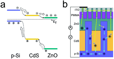 | ||
| Fig. 8 (a) Energy diagram of p-Si/n-CdS/n-ZnO heterojunction. The energy band structure of the nanorainforest solar cell shows a huge potential barrier between the adjacent layers for holes to tunnel through. For instance, the difference between the adjacent top of the valence band for Si/CdS and CdS/ZnO is ∼2 eV and ∼1 eV. (b) Scheme of charge transfer and collection in a nanorainforest solar cell. | ||
Charge carrier collection is a key factor in determining the overall efficiency of a solar cell. In thin film solar cell devices, light absorption and carrier collection are always in competition.18 Minority carriers more than one diffusion length from the p–n junction space charge region will have a large possibility for recombination rather than being collected. As a result, the thickness of the thin film cannot be very great. Nevertheless, a very thin film cannot absorb light efficiently. Introducing one-dimensional nanopillar arrays to the solar cell device could release such a constraint. Using the p–n junction of Si and ZnO as an example, with our purposely designed Si nanopillar arrays, which have a filling ratio of 50%, 500 nm in diameter, and ∼400 nm junction length with ZnO layer, the effective junction area between Si and ZnO has been increased four times more than that based on thin film architectures. Furthermore, because the Si nanopillar arrays were embedded through the CdS and ZnO layer in our multi-layer solar cell devices, and with the appropriate interdistance between adjacent Si nanopillars (∼500 nm), most of the photogenerated carriers are within the junction space charge region of Si nanopillars or within the minority diffusion length in the surrounding medium (CdS or ZnO), which could significantly enhance the carrier collection efficiency compared to thin film devices. Such enhanced carrier collection efficiency via introducing one-dimensional nanopillars was also discussed in detail in a recent review paper.18 The presence of Si nanopillar arrays is favorable for hole transport in our solar cells because the photogenerated holes in ZnO and CdS layer have to travel only a short pathway to reach the charge separating junction (the radial junction area of Si nanopillars and surrounding materials (ZnO or CdS)) without tunneling through the large potential barrier, see Fig. 8(a) and Fig. 8(b). Thus it can reduce the efficiency loss by shortening the required collection length. The photogenerated electrons in ZnO and CdS layer could be collected and transferred into ITO film (top electrode) via 1D ZnO nanowire arrays, as Fig. 8(b) indicates. Employing Si nanopillar arrays as charge transfer pathway, a smart integration of 1D nanostructure with multi-layer architecture, we provide an effective method to offer high carrier-collection efficiency and solve the current matching problems encountered in most thin-film-based multi-layer solar cells.
In general, most nanowire based solar cells suffer from a poor top-contact, which severely affects the device performance. The contact between ITO and ZnO nanowires has been significantly improved with PMMA as void-filling material since the contact area was significantly increased in this way. As shown in Table 1, the sheet resistivity of ZnO/PMMA/ITO is only 0.002 Ω cm, which is two orders of magnitude lower than that of ZnO/ITO (0.7 Ω cm), and four orders of magnitude lower than that of ZnO (21 Ω cm). Such low top contact resistance greatly increases the conversion efficiency from 0. 03–0.14%, and then to ∼0.52%.
Increasing the carrier density in ZnO and improving CdS crystal quality may further increase our device light conversion efficiency. The FF might be optimized by decreasing the resistance loss in the front and back electrodes, the interior carrier recombination in CdS nanoparticles and between crystal faces, and the resistance of each layer.
4. Conclusions
In summary, novel multi-layer nanorainforest solar cells based on p-Si nanopillar array/n-CdS nanoparticles/n-ZnO nanowire array heterostructures were achieved via a highly accessible, reproducible and controllable fabrication process. By choosing materials with proper bandgaps, an efficient light absorption and enhanced light harvesting were achieved by covering a wide range of the solar spectrum. Si nanopillar arrays were introduced as a direct conduction pathway for photon-generated charge efficient collection and transport. More importantly, the unique strategy using PMMA as a void-filling material to obtain a continuous, uniform and low resistance front electrode has significantly improved the overall light conversion efficiency. These results demonstrate that the nanorainforest solar cells, along with their large scale, low cost and easily controlled processing, may open up substantial opportunities for nanostructured photovoltaic devices.Acknowledgements
This project is financially supported by the National Natural Science Foundation of China (NSFC 50902004, 10974003 and 11023003), and National 973 projects (No.2007CB936202, 2009CB623703, MOST) from China's Ministry of Science and Technology and the Research Fund for the Doctoral Program of Higher Education. We acknowledge the International Science & Technology Cooperation Program of China Sino Swiss Science and Technology Cooperation Program (2010DFA01810) and FP7 EU IRSES project (MICROCARE) No.247641.References
- Y. Huang, X. F. Duan, Q. Q. Wei and C. M. Lieber, Science, 2001, 291, 630–633 CrossRef CAS.
- M. C. McAlpine, R. S. Friedman, S. Jin, K. H. Lin, W. U. Wang and C. M. Lieber, Nano Lett., 2003, 3, 1531–1535 CrossRef CAS.
- S. E. Han and G. Chen, Nano Lett., 2010, 10, 1012–1015 CrossRef CAS.
- Z. Y. Fan, H. Razavi, J. W. Do, A. Moriwaki, O. Ergen, Y. L. Chueh, P. W. Leu, J. C. Ho, T. Takahashi, L. A. Reichertz, S. Neale, K. Yu, M. Wu, J. W. Ager and A. Javey, Nat. Mater., 2009, 8, 648–653 CrossRef CAS.
- B. M. Kayes, H. A. Atwater and N. S. Lewis, J. Appl. Phys., 2005, 97, 114302 CrossRef.
- S. A. McDonald, G. Konstantatos, S. Zhang, P. W. Cyr, E. J. D. Klem, L. Levina and E. H. Sargent, Nat. Mater., 2005, 4, 138–142 CrossRef CAS.
- S. H. Ko, D. Lee, H. W. Kang, K. H. Nam, J. Y. Yeo, S. J. Hong, C. P. Grigoropoulos and H. J. Sung, Nano Lett., 2011, 11, 666–671 CrossRef CAS.
- O. L. Muskens, J. G. Rivas, R. E. Algra, E. P. A. M. Bakkers and A. Lagendijk, Nano Lett., 2008, 8, 2638–2642 CrossRef CAS.
- Q. Zhang, C. S. Dandeneau, X. Zhou and G. Cao, Adv. Mater., 2009, 21, 4087–4108 CrossRef CAS.
- K. Q. Peng and S. T. Lee, Adv. Mater., 2011, 23, 198–215 CrossRef CAS.
- H. Zhou, G. Fang, L. Yuan, C. Wang, X. Yang, H. Huang, C. Zhou and X. Zhao, Appl. Phys. Lett., 2009, 94, 013503 CrossRef.
- C.-Y. Huang, Y.-J. Yang, J.-Y. Chen, C.-H. Wang, Y.-F. Chen, L.-S. Hong, C.-S. Liu and C.-Y. Wu, Appl. Phys. Lett., 2010, 97, 013503 CrossRef.
- H.-D. Um, S. A. Moiz, K.-T. Park, J.-Y. Jung, S.-W. Jee, C. H. Ahn, D. C. Kim, H. K. Cho, D.-W. Kim and J.-H. Lee, Appl. Phys. Lett., 2011, 98, 033102 CrossRef.
- K. Sun, Y. Jing, N. Park, C. Li, Y. Bando and D. L. Wang, J. Am. Chem. Soc., 2010, 132, 15465–15467 CrossRef CAS.
- S. C. Lin, Y. L. Lee, C. H. Chang, Y. J. Shen and Y. M. Yang, Appl. Phys. Lett., 2007, 90, 143517 CrossRef.
- Y. Lee and C. Chang, J. Power Sources, 2008, 185, 584–588 CrossRef CAS.
- G. Peharz, G. Siefer and A. W. Bett, Sol. Energy, 2009, 83, 1588–1598 CrossRef CAS.
- Z. Fan, D. J. Ruebusch, A. A. Rathore, R. Kapadia, O. Ergen, P. W. Leu and A. Javey, Nano Res., 2009, 2, 829–843 CrossRef.
- Q. K. Shu, J. Q. Wei, H. W. Zhu, Z. Li, Y. Jia, X. C. Gui, N. Guo, X. M. Li, C. R. Ma and D. H. Wu, Nano Lett., 2009, 9, 4338–4342 CrossRef CAS.
- G. Kalita, S. Adhikari, H. R. Aryal, R. Afre, T. Soga, M. Sharon, W. Koichi and M. Umeno, J. Phys. D: Appl. Phys., 2009, 42, 115104 CrossRef.
- J.-Y. Wang, C.-Y. Lee, Y.-T. Chen, C.-T. Chen, Y.-L. Chen, C.-F. Lin and Y.-F. Chen, Appl. Phys. Lett., 2009, 95, 131117 CrossRef.
- E. C. Garnett and P. Yang, J. Am. Chem. Soc., 2008, 130, 9224–9225 CrossRef CAS.
- K. Peng, Y. Xu, Y. Wu, Y. Yan, S.-T. Lee and J. Zhu, Small, 2005, 1, 1062–1067 CrossRef CAS.
- K.-Q. Peng, X. Wang, X. Wu and S.-T. Lee, Appl. Phys. Lett., 2009, 95, 143119 CrossRef.
- Y. Wei, C. Xu, S. Xu, C. Li, W. Wu and Z. L. Wang, Nano Lett., 2010, 10, 2092–2096 CrossRef CAS.
- D. F. Liu, Y. J. Xiang, X. C. Wu, Z. X. Zhang, L. F. Liu, L. Song, X. W. Zhao, S. D. Luo, W. J. Ma, J. Shen, W. Y. Zhou, G. Wang, C. Y. Wang and S. S. Xie, Nano Lett., 2006, 6, 2375–2378 CrossRef CAS.
- K. Q. Peng, J. J. Hu, Y. J. Yan, Y. Wu, H. Fang, Y. Xu, S. T. Lee and J. Zhu, Adv. Funct. Mater., 2006, 16, 387–394 CrossRef CAS.
- Z. Huang, H. Fang and J. Zhu, Adv. Mater., 2007, 19, 744–748 CrossRef CAS.
- C. H. Chang and Y. L. Lee, Appl. Phys. Lett., 2007, 91, 053503 CrossRef.
- Y. C. Kong, D. P. Yu, B. Zhang, W. Fang and S. Q. Feng, Appl. Phys. Lett., 2001, 78, 407 CrossRef CAS.
- J. Ma, S. Y. Li, J. Q. Zhao and H. L. Ma, Thin Solid Films, 1997, 307, 200 CrossRef CAS.
- L. Hu and G. Chen, Nano Lett., 2007, 7, 3249–3252 CrossRef CAS.
- J. S. Li, H. Y. Yu, S. M. Wong, G. Zhang, X. W. Sun, P. G. Q. Lo and D. L. Kwong, Appl. Phys. Lett., 2009, 95, 033102 CrossRef.
- C. Battaglia, J. Escarré, K. Söderström, L. Erni, L. Ding, G.g. Bugnon, A. Billet, M. Boccard, L. Barraud, S. De Wolf, F.-J. Haug, M. Despeisse and C. Ballif, Nano Lett., 2011, 11, 661–665 CrossRef CAS.
Footnote |
| † Electronic supplementary information (ESI) available: EDS of the three layers; SEM images of ZnO layers with different thickness; SEM and TEM characterization of CdS nanoparticles. See DOI: 10.1039/c1nr11123j |
| This journal is © The Royal Society of Chemistry 2012 |