Excitonic properties of graphene-based materials
Min
Wang
abc and
Chang Ming
Li
*abc
aInstitute for Clean Energy & Advanced Materials, Southwest University, Chongqing, 400715, P.R. China. E-mail: ecmli@ntu.edu.sg; Fax: +65 67911761; Tel: +65 67904485
bSchool of Chemical and Biomedical Engineering, Nanyang Technological University, 70 Nanyang Drive, Singapore 637457
cCenter for Advanced Bionanosystems, Nanyang Technological University, 70 Nanyang Drive, Singapore 637457
First published on 30th September 2011
Abstract
First-principle density functional theory (DFT) calculations with quasiparticle corrections and many body effects are performed to study the electronic and optical properties of graphene-based materials. This review summarizes the excitonic properties including optical transition spectra and the distribution of exciton wavefunctions, thus providing the theoretical knowledge and predictions for promising optical applications of graphene materials.
 Min Wang | Dr Min Wang obtained her BS (2005) and MS (2007) at the University of Science and Technology in China, and PhD (2011) at the School of Chemical and Biomedical Engineering, Nanyang Technological University (NTU), Singapore. After completing a post-doctoral research project at NTU and a joint research project with Southwest University (SWU), China, she has become an associate professor at SWU. Her research is mainly focused on the investigations of nanoscale materials for their physical and chemical applications and future applications. |
 Chang Ming Li | Prof. Chang Ming Li received his PhD from Wuhan University in 1986 which was followed by post-doctoral research at UIUC (1988–1990), he then worked for US Motorola as a Science Advisory Board Associate, Distinguished Technical Staff and was senior manager for almost 10 years. He is currently head of the Bioengineering Division and director of the Centre for Advanced Bionanosystems at Nanyang Technological University, Singapore and is an associate editor of RSC Advances. His research includes nanostructured materials, green energy systems, electrochemistry and bionanotechnologies. He has published more than 280 journal papers and 84 patents. |
1. Introduction
Graphene, a two-dimensional single atomic layer of graphite, has attracted great interest1–6 due to its unique properties observed immediately after its first successful fabrication.7 Its novel electronic properties1 have great potential applications for nanoelectronics.8–13 However, due to its gapless property, modification of graphene is often needed to obtain different specific properties for various potential applications14–16 such as the magnetic ordering for spintronics17–22 and the electron/spin transport properties including negative differential resistance.23–25Optical properties are another important feature of graphene materials, for example photoluminescence and the absorptions or emissions. The modulated materials, with doping, defects, and absorption of atoms and molecules, have been experimentally26–29 successful leading to more interesting optical properties. To design new materials and extend new optical applications, the origins of optical and electronic properties are one of the main focuses of theoretical investigations.
Recently, the large difference between calculated Kohn–Sham band gaps and experimental results for nanostructures indicate that the Kohn–Sham eigenvalues from density functional theory (DFT) are inappropriate to describe optical excitations, due to the enhanced electron–electron interaction.30 Moreover, ground-state DFT cannot describe optical excitations properly, since an excited state (exciton) consists of a set of one excited electron and a hole at least, which is a two-particle problem,30 while DFT is based on a single-body theory. Thus, the approach of the first-principle calculation based on the many-body perturbation theory is needed and is more reliable.30 This review highlights recent theoretical works on graphene-based materials and illustrates new experimental investigations and perspectives as well.
2. Methodology
The approach to understand and predict the electronic and optical properties of nanostructures is based on the first-principle calculation associated with the many-body perturbation theory to accurately investigate situations in terms of three stages:31(i) The investigations always start with the correct atomic geometries in the electronic ground state. DFT within the local (spin) density approximation (L(S)DA) is also employed. By solving a set of effective, self-consistent, single-body equations, the ground state and electron density of a many-electron system can be determined. With consideration of the total energy versus the atomic coordinates, the stable atomic geometry is yielded.
(ii) Due to the good approximation of LDA wavefunctions with the quasiparticle ones, within the GW approximation the quasiparticle corrections to the LDA eigenvalues are evaluated for the self-energy operator. The GW approximation is an approximation to calculate self-energy of a many-body system in terms of the single particle Green function ‘G’ and the screened Coulomb interaction ‘W’. Additionally, within the plasmon-pole approximation, the screening is treated.32
(iii) By solving the Bethe–Salpeter equation (BSE) for the basis set of quasielectron and quasihole states, the electron-hole interaction and optical absorption spectra can be obtained. Within the random-phase approximation the static screening in the direct term is calculated.33
The electron–hole excited state can be represented as
 | (1) |
The excitonic wavefunction ASvck is obtained from the BSE
 | (2) |
The exciton wavefunction is given by
 | (3) |
Generally, the electron–hole interaction kernel Keh has two terms Kx and Kd, of which Kx is the exchange term containing the bare Coulomb interaction and determines the excitation spectrum,33 while Kd is the direct interaction term involving the screened Coulomb interaction, and is responsible for the attractive interactions of the electrons and holes and the formation of excitons.33 The following discussion on the electron–hole interaction of graphene-based materials is mainly focused on these two parts.
3. Graphene and bilayer graphene
With full relaxation, the calculated band structures of graphene and bilayer graphene are close to the Dirac point (plotted in Fig. 1(a) and (b)) within LDA and GW calculations. The LDA and GW Fermi velocities of graphene are estimated as 0.86 × 10⁶ m s−1 and 1.15 × 10⁶ m s−1 respectively, the latter one is in agreement with experimental data.5 Thus, for single-particle excitations, a significant self-energy correction is evaluated to the band velocity of the Dirac quasiparticles. | ||
| Fig. 1 Band structures of (a) graphene and (b) bilayer graphene plotted from LDA (black empty square) and GW corrections (blue filled square) respectively. Reprinted with permission from ref. 38. Copyright (2009) by The American Physical Society. | ||
The absorption spectra are focused on the light polarized parallel to the graphene plane. The absorbances of graphene and bilayer graphene are presented in Fig. 2(a) and (b) respectively, displaying similar excitonic effects. In the presence of an electron–hole interaction, the absorption peak of graphene arising from the intraband transitions is located at 4.55 eV, a redshift from the peak (5.15 eV) calculated without an electron–hole interaction. In addition, the line shape of the peak in the excitonic case is asymmetric in contrast to the symmetric peak resulting from the absence of excitonic effects. The prominent absorption peak of the bilayer graphene from the intraband transitions is around 5 eV without and 4.5 eV with excitonic effects. The peaks from bilayer graphene have similar origins to those of graphene. The small noticeable absorption peak of the bilayer graphene at 0.4 eV (Fig. 2 (b)) is contributed by the interband transitions near the Dirac point. The band structure of bilayer graphene is parabolic in shape near the Dirac point, resulting in a stronger screening than that in graphene. With excitonic effects, the redshift of the prominent absorption peak is to 450 meV in bilayer graphene compared to 600 meV in graphene. The calculated optical absorption of graphite is plotted in Fig. 2 (c) together with experimental data.39,40
 | ||
| Fig. 2 (a) Absorbance of (a) graphene, (b) bilayer graphene, and (c) imaginary part of the dielectric function of graphite with (red line) and without (blue dash-dot line) excitonic effects. The black line represents experimental data of graphite.39,40 Reprinted with permission from ref. 38. Copyright (2009) by The American Physical Society. | ||
4. Graphene nanoribbons (GNRs)
Graphene nanoribbons (GNRs) have gained great interest due to their unique electronic and optical properties. Two common types of GNRs are shown in Fig. 3. The left one has armchair-shaped edges with 11 carbon atoms along dimer lines, named 11-armchair GNR (11-AGNR), and the right one possesses zigzag-shaped edges with 6 carbon atoms along the y-axis, named 6-zigzag GNR (6-ZGNR). The edges in GNRs are passivated by hydrogen atoms. Within DFT41 and GW42 calculations, ZGNRs and AGNRs have a finite band gap with the possibility of full relaxation of the structures and spin polarization. | ||
| Fig. 3 Structures of (a) 11-AGNR possessing 11 carbon atoms (brown balls) along the dimer lines with the width w, and (b) 6-ZGNR having 6 atoms along the y-axis with the width w. The ribbons are passivated by hydrogen atoms (white balls) in both edges. Reprinted with permission from ref. 42. Copyright (2007) by The American Physical Society. | ||
AGNRs passivated by hydrogen atoms at the edges, possess sp2 bonds between carbon and hydrogen atoms, the electronic structures including the band gaps are dependent on the ribbon widths,41 further classifying these into three families: Na = 3p, 3p + 1 and 3p + 2, where p is a positive integer and Na is the number of dimer lines. In Fig. 4 (a), the band gaps from LDA and GW calculations clearly represent the size dependence. The hierarchy of band gaps was obtained as Eg3p+1 > Eg3p > Eg3p+2. The corrections by GW are from 0.5 to 3eV for the studied ribbons. The band gaps of ZGNRs calculated by LSDA and GW are shown in Fig. 4(b), they demonstrate that the ZGNR has an antiferromagnetic ground state with different spins occurring in two sublattices. The GW corrections to the LSDA band gaps are 0.8 to 1.5 eV in the studied cases. Additionally, the observed experimental result43 has supported the previous theoretical prediction41 — the energy gap decreases with the increase of the graphene ribbons' width. The detailed discussion of ZGNRs and AGNRs are described in section 5 and section 6 including their band structures.
 | ||
| Fig. 4 Variation of (a) band gaps with the width of AGNRs, and (b) direct band gaps and (c) the energy gap at the zone boundary with the width of ZGNRs. Reprinted with permission from ref. 42. Copyright (2007) by The American Physical Society. | ||
5. Zigzag graphene nanoribbons (ZGNRs)
Since ZGNRs possess a spin-polarized ground state with a finite band gap, the excitons in ZGNRs could have unique properties. As discussed above, the band gap is increased with GW corrections. The degenerated quasiparticle band structure of 8-ZGNR is shown in Fig. 5 (a). Enm denotes the interband transition and the bright exciton state from the nth valence band to the mth conduction band, marked as blue arrows in Fig. 5 (a). With and without the electron–hole interaction, the optical absorption spectrum of two ZGNRs are illustrated in Fig. 5 (b) and (c). The subscript i of Einm denotes the ith singlet exciton state of Enm. | ||
| Fig. 5 (a) Degenerate band structure of 8-ZGNR from GW calculations. Blue arrows represent the interband transitions. Optical absorption spectra of (b) 8-ZGNR and (c) 6-ZGNR with (red line) and without (blue line) electron–hole interaction. Reprinted with permission from ref. 44. Copyright (2008) by The American Physical Society. | ||
The binding energies of E111 and E121 are 0.67 eV and 0.71 eV respectively. The optical spectrum of 6-ZGNR shows a similar excitonic effect to that of 8-ZGNR. The unusual series of exciton states (E11i) can be used as a signature to identify the ZGNRs in experiments. The optical transition strength of an exciton state is strongly dependent on the light polarization direction. The dark exciton state D111 can become optically active with a small optical strength if the light polarization is perpendicular to the length of the ribbons but parallel to the plane of the ZGNRs. The binding energy of D111 is 0.47 eV for 8-ZGNR. The distribution of the dark exciton state D111 is plotted in Fig. 6 (a). In (b)–(e), a series of bright exciton states are illustrated. With the fixed holes marked as black spots, the electron distributions of exciton states display different features. In (a)–(d), the holes and electrons are spatially separated on two edges, while in (e), the electron distribution is extended on the same edge as the hole.
 | ||
| Fig. 6 Exciton wavefunction of 8-ZGNR for (a) D111, (b) E111, (c) E112, (d) E113, and (e) E121. The black spot shown is the fixed hole position. Reprinted with permission from ref. 44. Copyright (2008) The American Physical Society. | ||
The ground state of ZGNR is antiferromagnetic and has different spin orientations localized on different edges, thus the charge-transfer exciton nearly equally induces a spin transfer from either of the two edges. The sum of the magnetization remains zero along the ribbon width. However, with an external electric field, the degeneracy of up- and down-band states is lifted,45 then the magnetization is tuned, providing a way to control the distribution and magnetization of ZGNRs.
6. Armchair graphene nanoribbons (AGNRs)
The AGNRs have a family effect dependent on the number of dimer lines. To investigate the optical effects, two groups have independently reported their work: one investigated 8-,9-,10-AGNRs,36 and the other studied 10-,11-,12-AGNRs.46The quasiparticle band structure of 10-AGNR and the optical spectra of the three families of AGNR are plotted in Fig. 7. The first absorption peaks of 10-, 11-, and 12-AGNRs are located at the excitation energies of 1.8 eV, 0.25 eV, and 0.85 eV respectively. Since 10-AGNR has the largest band gap, the weakest screening occurs in the electron–hole Coulomb interaction out of three ribbons, yielding the largest exciton binding energy. In Fig. 7(b), the cyan curves are denoted as the interband optical absorption without electron-hole interaction. The interband transitions are marked by the arrows in Fig. 7(a). The first and second transitions E11 and E22 are almost degenerate (colored as cyan in Fig 7(b)) due to nearly having the same onsets of the two interbands. However, the dispersion of the energy bands is different, resulting in the different transitions. Hence, the degeneracy is broken with the consideration of the electron–hole interaction illustrated as the red line in Fig. 7(b). It should also be noted that the intensities of the two peaks are reversed with and without electron–hole interaction.
 | ||
| Fig. 7 (a) Quasiparticle band structure of the 10-AGNR. Optical spectra of (b) 10-, (c)11- and (d) 12-AGNRs with (red) and without (cyan) electron–hole interactions. Reprinted with permission from ref. 46. Copyright (2007) The American Chemical Society. | ||
The dark excitonic state denoted as D1 in Fig. 7 (b) is contributed to from the mixture of interband transitions E12 and E21, and D2 is the ‘excited state’ of D1 with a higher energy. The dark excitons are responsible for the optically inactive states degenerate with E11, since they provide a path for a nonradiative decay processes. This dark-state feature comes from the interband transitions between pairs of bands very close to each other, which are strongly dependent on the family N = 3p + 1 AGNRs, thus this is a common feature.
The exciton distributions of E111 and E221 in 10-AGNR as plotted in Fig. 8(a) and (b), have different fine structures which cover the length of the ribbons. A series of the projected exciton wavefunctions along the ribbons' directions are obtained with the integration of the electron coordinates in the perpendicular directions when keeping the hole fixed at the maximum density for the hole states (Fig. 8(c)–(f)). Comparing E111 with its “excited state” E112 of 10-AGNR, the later has a significantly larger extent. Comparing the extents of the first exciton states in 10-, 11-, and 12-AGNRs, 11-AGNR has the smallest binding energy.
 | ||
| Fig. 8 Exciton wavefunctions of 10-AGNR for (a) E111 and (b) E221. The black spot is denoted as the fixed hole in ribbons. (c)–(f) Exciton wavefunctions projected in the direction of the ribbon. Reprinted with permission from ref. 46. Copyright (2007) The American Chemical Society. | ||
AGNRs are still stable after removal of hydrogen atoms from the edges, which can be obtained with high temperatures or dehydrogenation treatments.47,48 Recent experiments also indicate that bare-edged ribbons can be formed from the unzipped carbon nanotubes.49,50 The optical absorption of clean-edged 9-AGNR is plotted in Fig. 9(c) with a comparison of hydrogen passivated 9-AGNR in (a). The modification of the AGNR can cause a redshift of the first excitonic peak located at 0.9 eV. The dark excitonic edge state is marked as the black arrow in (c). In all the studied bare-edged nanoribbons, a dark excitonic state exists with a binding energy of about 1.4–1.7 eV, with little dependence on the family or size effects.36 The quasiparticle band structure for the bare ribbon is represented in Fig. 9(d) and that for 9-AGNR with hydrogen is shown in (b). The difference between the energy band gaps is in agreement with the optical peaks.
 | ||
| Fig. 9 Optical absorption spectra with (black) and without (gray) exciton effects/quasiparticle band structures of (a)/(b) 9-AGNR and (c)/(d) 9-hydrogen-free AGNR. The black arrow points out the position of the dark exciton. Reprinted with permission from ref. 36. Copyright (2007) The American Physical Society. | ||
7. Edge and surface functionalized armchair graphene nanoribbons
F-passivated AGNRs have been investigated and show several interesting optical properties.37 A-Wm-B is used to depict the edge-modified AGNR, where A and B denote the edge-passivated atoms, and m is the number of dimer lines of AGNR used to characterize the width seen in Fig. 10(a). The family effect in H-passivated AGNRs has been discussed above. The trend of band gaps in H-passivated AGNRs is different from F-passivated ones though H- or F-passivated cases have nearly the most geometric carbon networks. The coupling of pz orbitals between two neighbouring carbon atoms can be perturbed due to the bonding atoms. The F-edged carbon atoms gain much less of a pz orbital than those in H-edged cases. To indicate the trend in F-edged cases, the effective width (EW) is introduced. Thus, F-W9-F and F-W10-F can be considered as F-EW7-F and F-EW8-F. The band gaps of these two cases are 0.89 and 0.86 eV, which can be presented as Eg(EW7;3p + 1) > Eg(EW8;3p + 2) and is in agreement with the reported family effect.41 This similar trend can work in the F-Wm-H and H-Wm-H structures. The optical spectra of the W9 and W10 series are plotted in Fig. 10(b) and also show a similar family trend. The shapes in each series are very similar, just having small shifts. The first optical transition energies in the W9 series are around 1 eV, while energies larger than 1 eV are in the W10 series. The exciton binding energies of F-W9-F and F-W10-F are 1.51 and 1.38 eV respectively, causing a larger distribution in F-W10-F than in F-W9-F. These two exciton wavefunctions are shown in Fig. 10(c), possessing different fine distributions. | ||
| Fig. 10 (a) Structures of edge-passivated AGNRs. (b) Optical absorption spectra of AGNRs. (c) Exciton wavefunctions of F-W9-F (left) and F-W10-F (right). Reprinted with permission from ref. 37. Copyright (2010) The American Chemical Society. | ||
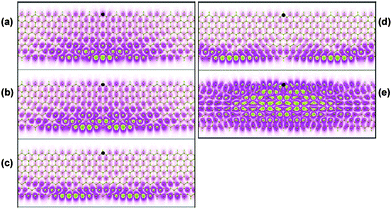
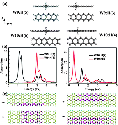
The AGNR can also be modulated by the surface functionalized atoms and molecules. Hydrogen adsorption on graphene has been experimentally explored. Here the optical properties in this kind of AGNR are discussed. Wm![[thin space (1/6-em)]](https://www.rsc.org/images/entities/char_2009.gif) :H(n) is used to denote the surface-modified AGNR, where m is the width of AGNR and n is the location of hydrogen atoms on the graphene ribbon along the dimer lines. Several W9 and W10 structures are shown in Fig. 11(a). The carbon atoms taking part in the surface absorption of hydrogen atoms possess sp3 hybridizations, resulting in the extension of carbon–carbon bonds. With consideration of sp2 networks, the effective width of Wm:H(n) reduces by two. Therefore for W9:H(n), the effective width is 7, which belongs to 3p + 1. The band gap in W9:H(n) is expected to be larger than that without hydrogen absorption in 9-AGNR. On the other hand, the effective width of W10:H(n) is 8, which belongs to 3p + 2, resulting in a decreased band gap. The different locations of hydrogen atoms on the AGNR's surfaces can modify the optical absorption spectra, shown in Fig. 11(b). The first optical transition energies of W9:H(3) and W9:H(5) are 1.13 and 2.96 eV respectively, while those of W10:H(4) and W10:H(6) are 1.37 and 0.54 eV respectively. For W9:H(n), the second optical absorption peaks are very close to the first ones. The W9:H(n) and W10:H(n) series have different distributions of excitonic wavefunctions, illustrated in Fig. 11(c). The black arrows point out the positions of hydrogen atoms on the surfaces, dividing the AGNR into two parts. In W9:H(3), the distribution of excitonic wavefunction is located only on the smaller sp2-network part. Since W9:H(5) has mirror symmetry, the two parts obtain similar distributions. In W10:H(n), the exictonic wavefunctions only cover the larger sp2-network parts.
:H(n) is used to denote the surface-modified AGNR, where m is the width of AGNR and n is the location of hydrogen atoms on the graphene ribbon along the dimer lines. Several W9 and W10 structures are shown in Fig. 11(a). The carbon atoms taking part in the surface absorption of hydrogen atoms possess sp3 hybridizations, resulting in the extension of carbon–carbon bonds. With consideration of sp2 networks, the effective width of Wm:H(n) reduces by two. Therefore for W9:H(n), the effective width is 7, which belongs to 3p + 1. The band gap in W9:H(n) is expected to be larger than that without hydrogen absorption in 9-AGNR. On the other hand, the effective width of W10:H(n) is 8, which belongs to 3p + 2, resulting in a decreased band gap. The different locations of hydrogen atoms on the AGNR's surfaces can modify the optical absorption spectra, shown in Fig. 11(b). The first optical transition energies of W9:H(3) and W9:H(5) are 1.13 and 2.96 eV respectively, while those of W10:H(4) and W10:H(6) are 1.37 and 0.54 eV respectively. For W9:H(n), the second optical absorption peaks are very close to the first ones. The W9:H(n) and W10:H(n) series have different distributions of excitonic wavefunctions, illustrated in Fig. 11(c). The black arrows point out the positions of hydrogen atoms on the surfaces, dividing the AGNR into two parts. In W9:H(3), the distribution of excitonic wavefunction is located only on the smaller sp2-network part. Since W9:H(5) has mirror symmetry, the two parts obtain similar distributions. In W10:H(n), the exictonic wavefunctions only cover the larger sp2-network parts.
 | ||
| Fig. 11 (a) Structures of surface-modified AGNRs. (b) Optical absorption spectra of surface-modified AGNRs. (c) Exciton wavefunctions of W9:H(3) (left, upper) and W9:H(5) (left, bottom), W10:H(4) (right, upper) and W10:H(6) (right, bottom). The arrows show the connected hydrogen atoms on the surfaces. Reprinted with permission from ref. 37. Copyright (2007) The American Chemical Society. | ||
8. Hydrogen saturated armchair graphene nanoribbons
A carbon atom can have sp3 hybridization to form four bonds. Thus it is possible for the edged carbon atoms in AGNRs to possess two hydrogen atoms for saturation. (n)H-W(Na)-(m)H is introduced to denote different AGNRs, where n and m are the numbers of the hydrogen atoms connected with carbon atoms at two edges and Na is the carbon atom number along the dimer line. The structures of H-W9-H, 2H-W9-H and 2H-W9-2H are schematically shown in Fig. 12 (a)–(c), respectively. 2H-W9-H is the half saturated 9-AGNR binding with two hydrogen atoms at one edge and one hydrogen atom at another edge. 2H-W9-2H is fully saturated by two hydrogen atoms at each edge. Hydrogen-passivated AGNRs only have sp2 hybridization, while half and full hydrogen-saturated ones have sp3 hybridizations. The “effective width”37 (EW) of sp2 networks is also useful for estimating the trend of band gaps in nH-W(Na)-mH AGNRs. Therefore the trend of Eg(2H-W9-2H) > Eg(H-W9-H) > Eg(2H-W9-H) can be presented as Eg(EW7; 3p + 1) > Eg(W9; 3p) > Eg(EW8; 3p + 2), which is in good agreement with the reported family effect.41 The optical absorption spectra of H-W9-H, 2H-W9-H and 2H-W9-2H AGNRs are plotted from the calculated data. The first optical transition energies for the three structures are located around 1.1 , 0.26 and 1.96 eV, respectively. Relating to the first strong optical transition peaks in Fig. 12(b), the respective excitonic wavefunctions are plotted under a real space in Fig. 12(c) to reveal a fundamental insight into the electron–hole interaction. Due to the discussed sp2 and sp3 effects of the edges in AGNRs, the distribution of exciton wavefunctions of H-W9-H covers two edges, that of 2H-W9-H is located on all sp2carbon atoms leaving the sp3 edge empty, and two edges of 2H-W9-2H are not covered by their exciton wavefunctions. | ||
| Fig. 12 (a) Schematic illustrations of H-W9-H, 2H-W9-H and 2H-W9-2H, left to right respectively. (b) Optical absorption spectra of H-W9-H (green), 2H-W9-H (red) and 2H-W9-2H (blue). (c) Exciton wavefunctions of H-W9-H, 2H-W9-H and 2H-W9-2H, top to bottom respectively. Reprinted with permission from ref. 51. Copyright (2011) The Royal Society of Chemistry. | ||
9. Summary and future perspective
The calculated optical properties of different graphene-based materials have been provided not only fundamental insights, but also different potential applications. Most of the carbon-based systems discussed above can be eventually obtained from graphite, which is abundant on the Earth. This particular characteristic makes carbon materials valuable for research and future industrial applications. The properties of graphene materials are currently under intense investigations to gain a deeper understanding of experiments and theories. The success of graphene materials in electronics and photonics experiments26–29 paves the way for graphene-based electronic devices in the future. Theoretical calculations and simulations can predict important properties whilst guiding critical experimental designs. Further theoretical understanding of the optoeletronic properties such as the origination of photoluminescence, the excitonic behaviour, and absorptions or emissions, is still needed for future applications.Acknowledgements
This work was financially supported by the Institute for Clean Energy & Advanced Materials, Southwest University, Chongqing, P. R. China and the Center for Advanced Bionanosystems, Nanyang Technological University, Singapore.Notes and references
- A. K. Geim and K. S. Novoselov, Nat. Mater., 2007, 6, 183 CrossRef CAS.
- A. H. Castro Neto, F. Guinea, N. M. R. Peres, K. S. Novoselov and A. K. Geim, Rev. Mod. Phys., 2009, 81, 109 CrossRef CAS.
- K. S. Novoselov, A. K. Geim, S. V. Morozov, D. Jiang, M. I. Katsnelson, I. V. Grigorieva, S. V. Dubonos and A. A. Firsov, Nature, 2005, 438, 197 CrossRef CAS.
- C. X. Guo, M. Wang, T. Chen, X. W. Lou and C. M. Li, Adv. Energy Mater., 2011 DOI:10.1002/aenm.201100223.
- Y. B. Zhang, Y. W. Tan, H. L. Stormer and P. Kim, Nature, 2005, 438, 201 CrossRef CAS.
- C. X. Guo and C. M. Li, Energy Environ. Sci., 2011 10.1039/c1ee01676h.
- K. S. Novoselov, A. K. Geim, S. V. Morozov, D. Jiang, Y. Zhang, S. V. Dubonos, I. V. Grigorieva and A. A. Firsov, Science, 2004, 306, 666 CrossRef CAS.
- Z. H. Chen, Y. M. Lin, M. J. Rooks and P. Avouris, Phys. E., 2007, 40, 228 CrossRef CAS.
- M. Y. Han, B. Ozyilmaz, Y. B. Zhang and P. Kim, Phys. Rev. Lett., 2007, 98, 206805 CrossRef.
- M. I. Katsnelson, K. S. Novoselov and A. K. Geim, Nat. Phys., 2006, 2, 620 CrossRef CAS.
- Y. M. Lin, K. A. Jenkins, A. Valdes-Garcia, J. P. Small, D. B. Farmer and P. Avouris, Nano Lett., 2009, 9, 422 CrossRef CAS.
- X. L. Feng, N. Chandrasekhar, H. B. Su and K. Mullen, Nano Lett., 2008, 8, 4259 CrossRef CAS.
- D. Abdula, T. Ozel, K. Kang, D. G. Cahill and M. Shim, J. Phys. Chem. C, 2008, 112, 20131 CAS.
- F. N. Xia, T. Mueller, Y. M. Lin, A. Valdes-Garcia and P. Avouris, Nat. Nanotechnol., 2009, 4, 839 CrossRef CAS.
- C. X. Guo, H. B. Yang, Z. M. Sheng, Z. S. Lu, Q. L. Song and C. M. Li, Angew. Chem., Int. Ed., 2010, 49, 3014 CrossRef CAS.
- C. X. Guo, X. T. Zheng, Z. S. Lu, X. W. Lou and C. M. Li, Adv. Mater., 2010, 22, 5164 CrossRef CAS.
- D. W. Boukhvalov, M. I. Katsnelson and A. I. Lichtenstein, Phys. Rev. B: Condens. Matter Mater. Phys., 2008, 77, 035427 CrossRef.
- D. W. Boukhvalov and M. I. Katsnelson, Nano Lett., 2008, 8, 4373 CrossRef CAS.
- M. Wang and C. M. Li, New J. Phys., 2010, 12, 083040 CrossRef.
- Y. C. Huang, C. P. Chang and M. F. Lin, Nanotechnology, 2007, 18, 495401 CrossRef CAS.
- M. Wang and C. M. Li, Phys. Chem. Chem. Phys., 2011, 13, 5945 RSC.
- M. Wang, W. Huang, M. B. Chan-Park and C. M. Li, Nanotechnology, 2011, 22, 105702 CrossRef.
- W. Y. Kim and K. S. Kim, Nat. Nanotechnol., 2008, 3, 408 CrossRef CAS.
- H. Ren, Q. X. Li, Y. Luo and J. L. Yang, Appl. Phys. Lett., 2009, 94, 173110 CrossRef.
- M. Wang and C. M. Li, Phys. Chem. Chem. Phys., 2011, 13, 1413 RSC.
- P. Blake, E. W. Hill, A. H. C. Neto, K. S. Novoselov, D. Jiang, R. Yang, T. J. Booth and A. K. Geim, Appl. Phys. Lett., 2007, 91, 063124 CrossRef.
- T. Gokus, R. R. Nair, A. Bonetti, M. Bohmler, A. Lombardo, K. S. Novoselov, A. K. Geim, A. C. Ferrari and A. Hartschuh, ACS Nano, 2009, 3, 3963 CrossRef CAS.
- K. P. Loh, Q. L. Bao, G. Eda and M. Chhowalla, Nat. Chem., 2010, 2, 1015 CrossRef CAS.
- F. Bonaccorso, Z. Sun, T. Hasan and A. C. Ferrari, Nat. Photonics, 2010, 4, 611 CrossRef CAS.
- S. G. Louie, Conceptual Foundations of Materials: A Standard Model for Ground- and Excited-State Properties; Contemporary Concepts of Condensed Matter Science, Elseiver, New York, 2006 Search PubMed.
- G. Onida, L. Reining and A. Rubio, Rev. Mod. Phys., 2002, 74, 601 CrossRef CAS.
- R. W. Godby and R. J. Needs, Phys. Rev. Lett., 1989, 62, 1169 CrossRef.
- M. Rohlfing and S. G. Louie, Phys. Rev. B: Condens. Matter, 2000, 62, 4927 CrossRef CAS.
- A. G. Marinopoulos, L. Reining, A. Rubio and N. Vast, Phys. Rev. Lett., 2003, 91, 046402 CrossRef CAS.
- C. A. Rozzi, D. Varsano, A. Marini, E. K. U. Gross and A. Rubio, Phys. Rev. B: Condens. Matter Mater. Phys., 2006, 73, 205119 CrossRef.
- D. Prezzi, D. Varsano, A. Ruini, A. Marini and E. Molinari, Phys. Rev. B: Condens. Matter Mater. Phys., 2008, 77, 041404 CrossRef.
- X. Zhu and H. B. Su, J. Phys. Chem. C, 2010, 114, 17257 CAS.
- L. Yang, J. Deslippe, C.-H. Park, M. L. Cohen and S. G. Louie, Phys. Rev. Lett., 2009, 103, 186802 CrossRef.
- E. A. Taft and H. R. Philipp, Phys. Rev., 1965, 138, A197 CrossRef.
- A. B. Djurisic and E. H. Li, J. Appl. Phys., 1999, 85, 7404 CrossRef CAS.
- Y. W. Son, M. L. Cohen and S. G. Louie, Phys. Rev. Lett., 2006, 97, 216803 CrossRef.
- L. Yang, C.-H. Park, Y.-W. Son, M. L. Cohen and S. G. Louie, Phys. Rev. Lett., 2007, 99, 186801 CrossRef.
- M. Y. Han, B. Ozyilmaz, Y. B. Zhang and P. Kim, Phys. Rev. Lett., 2007, 98 Search PubMed.
- L. Yang, M. L. Cohen and S. G. Louie, Phys. Rev. Lett., 2008, 101, 186401 CrossRef.
- Y. W. Son, M. L. Cohen and S. G. Louie, Nature, 2006, 444, 347 CrossRef CAS.
- L. Yang, M. L. Cohen and S. G. Louie, Nano Lett., 2007, 7, 3112 CrossRef CAS.
- T. Kawai, Y. Miyamoto, O. Sugino and Y. Koga, Phys. Rev. B: Condens. Matter Mater. Phys., 2000, 62, R16349 CrossRef CAS.
- V. Barone, O. Hod and G. E. Scuseria, Nano Lett., 2006, 6, 2748 CrossRef CAS.
- L. Y. Jiao, L. Zhang, X. R. Wang, G. Diankov and H. J. Dai, Nature, 2009, 458, 877 CrossRef CAS.
- D. V. Kosynkin, A. L. Higginbotham, A. Sinitskii, J. R. Lomeda, A. Dimiev, B. K. Price and J. M. Tour, Nature, 2009, 458, 872 CrossRef CAS.
- M. Wang and C. M. Li, Nanoscale, 2011, 3, 2324 RSC.
| This journal is © The Royal Society of Chemistry 2012 |