Research highlights
Šeila
Selimović
ab,
Mehmet R.
Dokmeci
ab and
Ali
Khademhosseini
*abcd
aCenter for Biomedical Engineering, Department of Medicine, Brigham and Women's Hospital, Harvard Medical School, Cambridge, Massachusetts 02139, U. S. A. E-mail: alik@rics.bwh.harvard.edu
bHarvard-MIT Division of Health Sciences and Technology, Massachusetts Institute of Technology, Cambridge, Massachusetts 02139, U. S. A.
cWyss Institute for Biologically Inspired Engineering, Harvard University, Boston, Massachusetts 02115, U. S. A.
dWorld Premier International – Advanced Institute for Materials Research (WPI-AIMR), Tohoku University, Sendai 980-8577, Japan
First published on 15th February 2012
Modeling embryonic development on a microchip
Embryonic development is driven by primordial cell fate decisions such as self-renewal and differentiation that generate spatially patterned tissues. These decisions are influenced by the biochemical cues in the cellular environment as well as physical factors such as the topography and stiffness of the extracellular matrix (ECM).1To understand the mechanisms that control embryonic patterning, it is important to separate the experimental factors driving cellular organization from other environmental factors. Due to their ability to control the microenvironment of cells with precise control, microscale techniques lend themselves to this task.3 In one recent example, a spatially patterned platform to investigate mechanisms involved in embryonic development has been developed.2
In their recent work, Toh et al.2 applied two simple microscale patterning techniques—stencil cell patterning and bio flip chip (BFC)—to spatially organize the stem cell microenvironment. Combining these two processes resulted in a method they termed Differential Environmental Spacial Patterning (δESP), which allowed the researchers to deposit complex and precise shapes of more than 2 cell types or ECMs on a substrate and then localize stem cells on top of the resulting patterns (Fig. 1A,B).
 | ||
| Fig. 1 Differential environmental spatial patterning (δESP) process: concept (A) and assembly of the experimental platform (B). (C) Mouse embryonic stem cell colony patterned on two substrates. (D) Differentiation (Nestin+) and self-renewal (Sox 2+) markers expressed after a 5 day culture on different substrates. Scale bars: (B) 1 cm; (C,D) 500 μm. Figure adapted and reprinted with permission from the Royal Society of Chemistry from Toh et al.2 | ||
The first question that was addressed using this platform was whether externally controlled local microenvironments could alter embryonic stem cell (ESC) fate. Here, mouse ESCs were cultured on either gelatin or mouse embryonic fibroblasts, or a spatially organized mixture of both (Fig. 1C). As expected from control experiments, ESCs cultured on either pure gelatin or the fibroblasts expressed predominantly neural (Nestin+) or self-renewal (Sox 2+) markers, respectively. The occurrence of both markers were radially symmetric. However, when cultured on the differentially patterned substrate, the ESCs differentiated asymmetrically along an axis normal to the pattern boundary (Fig. 1D). Changing the relative ratios of gelatin to fibroblasts did not affect the location of phenotype transition (∼400 μm from the pattern boundary). This observation indicated that the internal kinetics of cell fate were unaffected by the external spatial organization on the substrate.
Subsequently, the authors developed a model of the proximal/distal axis formation in a mouse embryo (at embryonic stage E5.5) by spatially segregating stem cells derived from extra embryonic ectoderm (ExE, proximal) and visceral endoderm (VE, distal) cell lineages with respect to a large aggregate of mouse ESCs. Control experiments (cell cultures on either ExE or VE containing substrates) yielded spatially undifferentiated expression of proximal and distal markers. ESCs cultured across the interface of ExE and VE regions, however, exhibited spatially varied differentiation patterns. Proximal markers were strongly expressed on the ExE substrate while distal markers were more highly expressed on the VE substrate. Thus, the cells cultured on different substrates were induced to express different differentiation markers.
The system developed in this work enables decoupling of the effects of spatial cues and internal cell kinetics on stem cell differentiation. Given the importance of stem cells for regenerative medicine applications, the ability to understand and regulate the behavior of these cells is a highly important scientific endeavour. Thus, the application of this microscale technology to stem cell studies offers a promising approach to extend our understanding of the differentiation mechanisms and embryonic development.
Compound μ-lenses
Naturally occurring structures ranging from lotus leaves and fish scales to moth's eyes have inspired artificial approaches for creating superhydrophobic materials, anti-reflective coatings and numerous other functional materials.4 Recently, Lee and coworkers have developed a microscale lens-on-lens array modeled after the compound eye of an insect to fabricate functional optical materials.Contrary to conventional methods for fabricating compound lenses, e.g. photolithography, surface wrinkling, or self-organization inside droplets, which resulted in either planar lenses or uncontrolled lens curvatures, Park et al.5 developed a novel yet simple technique for manufacturing 2D lens-on-lens arrays that are highly similar to their natural counterparts. The researchers placed a polycarbonate film on a photolithographically prepared silicon substrate containing a 2D array of deep, vertical cylindrical channels (Fig. 2a). Upon heating the material to a temperature above its glass transition temperature, they applied a pressure difference between the inside of the microchannels and the outside of the thermoplastic polymer film. When the pressure inside the cylindrical channels was lower than outside, the film flowed into the channels. After 3 min, the film was cooled and hardened to yield a 2D array of convex microlenses. In the other case, when the outside pressure was lower than the pressure inside the channels, concave microlens arrays (MLA) were formed.
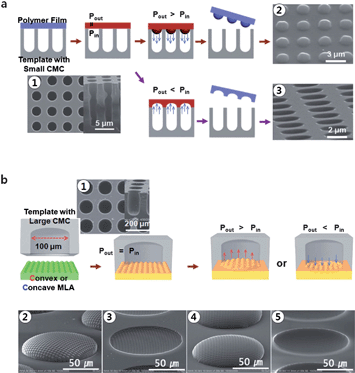 | ||
| Fig. 2 Fabrication scheme of the microlens array (MLA) (a) and the micro lens-on-lens array (MLLA) (b), for both convex and concave lenses. Figure reprinted with permission from the Royal Society of Chemistry from Park et al.5 | ||
By using this approach, microlenses that were 100 μm in diameter with a spacing of 150 μm were routinely produced. Moreover, lenses as small as 2 μm could be fabricated. The radius of curvature and the focal length of the lenses were found to be dependent on the melting time. As the polycarbonate film was heated for a longer time, the deeper it could flow into the cylindrical channels resulting in the formation of higher aspect ratio features.
To form microscale lens-on-lens arrays (MLLA), the process described above was repeated with the shaped film, however this time a silicon substrate with much wider cylindrical channels (100 μm to 1000 μm diameter) was used (Fig. 2b). This enabled the formation of convex-on-convex, concave-on-concave, convex-on-concave, and concave-on-convex compound lenses. During the second melting process, the microlenses fabricated earlier flowed independently, however, their height changed by only 10% during the 10 to 20 min of flow. This parameter was also included in the mathematical description of the polymer flow, which yielded highly predictable fabrication results. Finally, the imaging capabilities of both smaller and larger lenses were independently observed. All but the smallest microlenses (2 μm diameter) could faithfully form images of a patterned film, although the smallest lenses were also able to record specific light intensity patterns.
The ability to rapidly manufacture four different types of compound optical systems, each with different light transmission properties, while using a single experimental setup, opens a path to a new generation of functional optical films. By having a much wider field of view than spherical lenses and fabricated from inert polymeric materials, these compound lenses could be incorporated in a variety of lab-on-a-chip devices for improved imaging capabilities.
A portable, affordable photolithography system
Microfluidics and other microscale technologies are helpful in studying physical, chemical, and biological systems in a controlled fashion. In addition to a vast reduction in experiment duration and the quantity of reagents, the low cost of materials for fabricating lab-on-a-chip devices make them appealing for various experimental platforms. Yet, a major barrier to entry in this field remains the need for cleanrooms and expensive photolithographic systems for patterning of device templates and masters.Efforts have been made to create affordable UV-exposure units which utilize projectors to resize and project digital images on a photosensitive material, however, these systems still require several optical components and have relatively low resolution (∼10 μm).6,7 An even simpler, portable setup has recently been introduced by Huntington and Odom.8 Here, the authors utilized battery powered UV light emitting diodes (LEDs) and flashlights as the light source to pattern different types of photoresists.
Two hundred GaN-based LEDs were connected in parallel on a circuit board. The diodes emitted at 405 nm and were compatible with g-line photoresists, absorbing at 350 to 450 nm. The system was powered by eight AA (6V) batteries and could run continuously for 75 min. A ground glass plate was placed between the diodes and the sample to diffuse the light. By using this setup, the light intensity varied across the illuminated area (64 cm2) by only 4%, which is comparable to state-of-the-art exposure systems using Hg or HgXe light sources. Yet the LED-based system was assembled for less than $400 USD, which is at least two orders of magnitude lower in cost than factory made exposure units. In addition, the LEDs reached maximum optical intensity within a short time (<300ms) and consumed less than 6 W.
The LED exposure source enabled high precision patterning. By using this approach, 750 nm wide and 500 nm tall lines with a 2 μm pitch were reliably patterned through a Cr mask. When tested with poly(dimethylsiloxane) masks, the minimum feature size that was produced reliably was 180 nm (diameter) with a 400 nm pitch and a 200 nm height. Noticeably, the patterning was completed not in a cleanroom, but an ordinary research laboratory, and the patterned features did not have any defects that could be attributed to dust particles and other contaminants.
To enable the use of this system for photoresists such as SU-8, the LED array was replaced by a commercially available flashlight, emitting at 365 nm. By using this system a silicon wafer coated with SU-8 was patterned through a transparency mask to generate 50 μm wide channel features that were 25 μm tall. Because of the low output power of the flashlight, the exposure time was relatively long (40 min). Considering that in most cases a single master needs to be produced once and can be reused many times (often ∼50 times or more) to fabricate elastomeric replicates, this exposure time is not a serious disadvantage of the system. Another noteworthy factor is the low cost of the system components.
The described UV exposure system is affordable and simple to build, and as such is a useful system for researchers without access to factory-made photolithography equipment and expensive cleanrooms. The resolution of this exposure system is several hundred nm, making this system also appealing to researchers who require complex and highly precise device features. The sole disadvantage of the system is the lack of an alignment stage. As such, only a single exposure step can be completed on one substrate. However, adding an xyz-controllable robotic stage and a 10x objective should be sufficient to vastly increase the usefulness of the proposed exposure platform.
References
- M. Zernicka-Goetz, S. A. Morris and A. W. Bruce, Making a firm decision: multifaceted regulation of cell fate in the early mouse embryo, Nat. Rev. Genet., 2009, 10(7), 467–477 CrossRef CAS.
- Y.-C. Toh, et al., Spatially organized in vitro models instruct asymmetric stem cell differentiation, Integr. Biol., 2011, 3, 1179–1187 RSC.
- H. Qi, et al., Patterned differentiation of individual embryoid bodies in spatially organized 3D hybrid microgels, Adv. Mater., 2010, 22(46), 5276–81 CrossRef CAS.
- B. Bhushan, Biomimetics: lessons from nature - an overview, Philos. Trans. R. Soc. London, Ser. A, 2009, 367(1893), 1445–1486 CrossRef CAS.
- B. G. Park, et al., Micro lens-on-lens array, Soft Matter, 2012, 8, 1751–1755 RSC.
- J. D. Musgraves, B. T. Close and D. M. Tanenbaum, A maskless photolithographic prototyping system using a low-cost consumer projector and a microscope, Am. J. Phys., 2005, 73(10), 980–984 CrossRef.
- K. Itoga, et al., Second-Generation Maskless Photolithography Device for Surface Micropatterning and Microfluidic Channel Fabrication, Anal. Chem., 2008, 80(4), 1323–1327 CrossRef CAS.
- M. D. Huntington and T. W. Odom, A portable, benchtop photolithography system based on a solid-state light source, Small, 2011, 7(22), 3144–3147 CrossRef CAS.
| This journal is © The Royal Society of Chemistry 2012 |