Microfluidic sensing devices employing in situ-formed liquid crystal thin film for detection of biochemical interactions†‡
Ye
Liu
a,
Daming
Cheng
b,
I-Hsin
Lin
c,
Nicholas L.
Abbott
bc and
Hongrui
Jiang
*abd
aDepartment of Electrical and Computer Engineering, University of Wisconsin-Madison, 1415 Engineering Drive, Madison, WI 53706, USA. E-mail: hongrui@engr.wisc.edu; Fax: 1-608-262-1267; Tel: 1-608-265-9418
bMaterials Science Program, University of Wisconsin-Madison, 1415 Engineering Drive, Madison, WI 53706, USA
cDepartment of Chemical and Biological Engineering, University of Wisconsin-Madison, 1415 Engineering Drive, Madison, WI 53706, USA
dDepartment of Biomedical Engineering, University of Wisconsin-Madison, 1550 Engineering Drive, Madison, WI 53706, USA
First published on 21st June 2012
Abstract
Although biochemical sensing using liquid crystals (LC) has been demonstrated, relatively little attention has been paid towards the fabrication of in situ-formed LC sensing devices. Herein, we demonstrate a highly reproducible method to create uniform LC thin film on treated substrates, as needed, for LC sensing. We use shear forces generated by the laminar flow of aqueous liquid within a microfluidic channel to create LC thin films stabilized within microfabricated structures. The orientational response of the LC thin films to targeted analytes in aqueous phases was transduced and amplified by the optical birefringence of the LC thin films. The biochemical sensing capability of our sensing devices was demonstrated through experiments employing two chemical systems: dodecyl trimethylammonium bromide (DTAB) dissolved in an aqueous solution, and the hydrolysis of phospholipids by the enzyme phospholipase A2 (PLA2).
Introduction
Highly sensitive, portable and cost-effective bio/chemical sensors are critical elements for various applications, such as chemical warfare agent detection and point-of-care diagnostics.1,2 Recently, the long-range orientational ordering of liquid crystals (LCs) has been demonstrated to provide one effective approach for the implementation of such sensors,3–5 particularly based on the effects of interfacial binding of biomolecules.6–9 Due to the high sensitivity of LCs to the target and absence of the need for a label, this approach has been demonstrated to be an effective method for real-time, label-free and high sensitivity sensing. For example, vapor-phase analyte concentrations in the parts-per-billion range have been successfully detected.5,10 LC has also been exploited to report the reorganization of lipid monolayers driven by specific lipid–protein binding events.11 Other materials, such as functional pH-dependent amphiphilic polymers, have also been combined with LCs to transduce the environmental information into optical signals.12 In order to transduce and amplify interfacial molecular interactions into optical signals utilizing LCs, one of the essential steps is to create a stable LC thin film, which is supported on a solid surface to provide a pre-defined alignment to the LC. Because the alignment of LC is fixed at the solid-LC interface, changes in the ordering of the LC within the thin film can be attributed to interactions between the LC film and targeted analytes at the free-LC film interface. Changes in the ordering of the LC lead to changes in the optical properties of the LC film, which are easily transduced via the transmission of polarized light through the LC film. However, as discussed, such LC thin films need to be “open”, i.e. have free surfaces that can be exposed to and interact with analytes. Thus fabrication methods for conventional LC devices, though relatively mature, (for example, LC vacuum injection for LC display manufacturing) are not applicable for LC sensing devices. Current effective approaches to form LC thin films for sensing include manually pipetting LC into the square openings of a transmission electronic microscopy (TEM) grid,8,9 or using arrays of microfabricated pillars to stabilize thin LC film.5 Those approaches, though producing high-quality LC thin films, require manual handling of LCs, and are time consuming and require skilled personnel. Processes that lead to uniform and reproducible LC thin films are still sought, particularly in situ forming schemes, which do not rely on manual procedures.We previously reported a preliminary study of in situ-formed LC thin films in microfluidic devices.13 Herein, we present a more detailed study of this approach. The preparation of the LC-thin film as well as the in situ sensing process of the devices is driven by laminar flows in the microchannel, which can be precisely controlled by pre-defined flow rates of the laminar flows with a programmable syringe pump. Thus, the need for manual handling is eliminated. In particular, after filling the channel with LC, the laminar flow of the aqueous target phase is introduced into the channel at a high flow rate. The shear force of the laminar flow removes the bulk LC in the micro-sensing channel, and creates LC thin films in a supporting structure. The birefringence of the LC thin film can then be monitored by polarized optical microscopy (POM). The thickness and quality of the LC thin film were calculated by a computational fluid dynamics (CFD) simulation and then demonstrated by subsequent testing with two model chemical systems. One of the model systems reported the existence of dodecyl trimethylammonium halide (DTAB) in the deionized (DI) water phase.14,15 The second system involved binding of phospholipase A2 (PLA2) to a monolayer of phospholipids hosted at the LC-aqueous interface8,16 and subsequent enzymatic hydrolysis of the phospholipid.
Materials and methods
Chemical and hardware materials
Liquid crystal, 5CB and 1-decanethiol [CH3(C9H18)SH], 96%, L-α-dilauroyl phosphatidylcholine (L-DLPC), N,N-dimethyl-N-octadecyl-3-amino-propyltrimethoxysilyl chloride (DMOAP) and phospholipase A2 (PLA2) from Naja mossambica mossambica were purchased from Sigma-Aldrich (St. Louis, MO, USA). N-hexadecyl mercaptan [CH3(C15H30)SH], 92% was purchased from Acros Organics (Geel, Belgium). Glass slides were purchased from Fisher Scientific (Pittsburgh, PA, USA). Microfab NI 100 make-up solution and Microfab NI 100 wetting agent were purchased from Enthone-OMI (West Haven, CT, USA). High purity Ni gauze, #39704 was purchased from Alfa Aesar (Ward Hill, MA, USA). Positive photoresist (PR), AZ P4620, was purchased from Clariant Corporation (Somerville, NJ, USA). Double adhesive spacer (250-μm-thick) was acquired from 3M Co. (St. Paul, MN, USA). Ethyl vinyl acetate microbore tubings were purchased from Cole Parmer Co. (Vernon Hills, IL, USA).Principles of device preparation and operation
The concept and structure of the sensing device is shown in Fig. 1. As shown in Fig. 1(a), an LC supporting structure is integrated into a microfluidic sensing channel. The supporting grid structure consists of hexagonal cells separated by Ni bars, as shown in the blow up image. The height of the Ni grid is ∼30 μm, and the diameter of a single hexagonal cell is ∼0.3 mm. The hexagonal cell array is confined by 0.3 mm width Ni lines in a 3 mm × 3 mm square area. The dimensions listed above are chosen so as to provide the required LC film thickness and lead to uniform orientation of the LC (as the exposing area of each cell is small). The microchannel has one inlet for LC, one inlet for an aqueous target phase and one inlet for another aqueous target phase. The whole device is positioned between two crossed linear polarizing filters, with a white light source illuminating from bottom. Thus, the birefringence of the LC thin film can be monitored by a microscope (Fig. 1(b)). | ||
| Fig. 1 Schematic illustration and photographs of the sensing device. (a) Top view of the device structure. The square structure with hexagonal grid is electroplated on the substrate. The microfluidic channel is created on a glass substrate with a 250 μm thick adhesive spacer. (b) Images of the device mounted on a POM. (c) Schematic of the sensing setup. The figure portion in the middle shows the side view of the device along AA′. Pre-filled 5CB in the sensing channel is pushed away by the laminar flow of aqueous liquid. The shear force of the flow forms LC-aqueous interface at the top of the grid structure. The device is placed between two crossed polarizers and illuminated from bottom. | ||
As described above, for effective sensing with LC thin films, we need to: first, pre-treat the supporting substrate so that the substrate–LC interface provides a pre-defined alignment/orientation to the LC; second, limit the thickness of the LC film below 100 μm (as described in past studies5,10) so that the interfaces of the LC will control the orientation of the entire LC film. Thus, the optical properties of the LC thin film will be solely determined by the LC orientation at the LC–aqueous target phase interface.
Deposition of self-assembled monolayers (SAMs) on a substrate is an effective way to anchor the orientation of LC at a substrate–LC interface.17,18 By depositing a 20 nm layer of gold and applying a mixture of alkanethiols, a mixed alkanethiol SAM is formed on the substrate such that the LC mesogens contacting the SAM assume a homeotropic alignment. The requirement for the semi-transparent gold layer, however, complicates the fabrication process and increases the cost. Moreover, the transmittance of the gold layer in the visible light region is less than 50%.18
DMOAP, in contrast, is an alkoxysilane surfactant used commonly for treating metal-oxide/glass so that the LC at the interface assumes homeotropic alignment.19,20,21 After a simple dipping and rinsing process, a silane layer applied to the glass substrate is permanently bonded to the substrate in such a manner that the orienting groups of the silane coupling agent molecules are free to interact with and align neighbouring LC molecules.22 Moreover, the monolayer of DMOAP does not significantly reduce the transmittance of visible light. Guided by the above observation, we fabricated sensing devices functionalized using both gold/alkanethiol SAMs and DMOAP coatings, and demonstrated that they exhibit similar performances. This way, we also demonstrated that our sensing device is compatible with multiple coating methods. Thus, if a target analyte interacts with alkanethiols, we can alternatively use alkoxysilane coating on our device, and vice versa.
Due to the small dimension of the microfluidic channel (∼ 4 mm × 3 mm × 0.25 mm), the behaviour of the infusing liquid usually falls into the laminar flow regime. Thus, phenomena associated with the laminar flow can be used to create the LC thin film as well as the LC-target phase interface. As shown in the side view (middle image) in Fig. 1(c), after filling the channel with LC, the flow of the aqueous target phase is introduced into the channel at a high flow rate. The shearing force of the laminar flow removes the bulk LC in the micro sensing channel, and leaves LC thin films in the supporting structure. The thickness of the LC thin film is about the height of the supporting Ni grid, i.e. ∼ 30 μm.
Fabrication of the sensing devices
The fabrication process of the devices is illustrated in Fig. 2. The process started from microscopy glass slides with seed layers of titanium/copper/titanium (Ti/Cu/Ti, 225/300/350 Å). The seed layers were coated using a CHA-600 e-beam evaporator (CHA Industris, Fremont, CA, USA). A photoresist (PR) mold was patterned on the Ti/Cu/Ti-coated glass slide to define the Ni-plated grid structure. Two layers of PR were spin-coated on top of the seed layers so that a 40 μm thick PR mold was formed. To pattern the PR, a printed transparent film (Imagesetter, Inc. Madison, WI, USA) was used as the mask. An ultraviolet (UV) lamp (OmniCureTM Series 2000, EXFO Photonic Solutions Inc. Ontario, Canada) was used to expose PR at the intensity of 24.6 mW cm−2 for 80 s (Fig. 2(b)). After PR patterning and developing, the top Ti layer that was not covered by PR was removed by buffered oxide etchant (BOE, 100![[thin space (1/6-em)]](https://www.rsc.org/images/entities/char_2009.gif) :1), leaving Cu exposed (Fig. 2(c)).
:1), leaving Cu exposed (Fig. 2(c)).
 | ||
| Fig. 2 Fabrication process for the sensing devices. (a) The process starts from a glass substrate coated with Ti/Cu/Ti as seed layers for following electroplating; (b) Two layers of photoresist (PR) (∼ 40 μm in thickness) are spin-coated on the seed layer and the pattern of the nickel grid is defined by UV exposure; (c) The pattern is then transferred by developing PR. Cu seed layer is exposed by etching Ti. (d) 30 μm of Ni is electroplated with photoresist as a mold; (e) Remove PR with acetone, followed by removal of the exposed seed layers with buffered oxide etchant (BOE) and Cu etchant; (f1) 20 nm translucent Au layer is evaporated on the structure. Mixed alkanethiol SAM is formed on top of the Au layer; or (f2) a layer of DMOAP is directly coated on the glass substrate; (g) The substrate with the structure is bonded with a cover glass slide using 250 μm adhesive spacers. | ||
The Ni electroplating bath, agitated at a constant 200 rpm, consisted of 1:0.01 Microfab NI 100 make-up solution and Microfab NI 100 wetting agent. The bath temperature, maintained at a temperature of 50 ± 1 °C, was continuously monitored by a type-K thermocouple probe (Omega HH506A, OMEGA Engineering, Inc, Stamford, CT, USA). Ni gauze was used as the Ni source (anode) for electroplating. Ni was electroplated onto the active sites on the glass slide (cathode; where Cu was exposed) at a rate of approximately 0.60–1.00 μm min−1 so that Ni structure with a thickness of 25–30 μm was achieved in ∼30 min (Fig. 2(d)). After the completion of Ni electroplating, the PR mold was removed by acetone. The Ti/Cu/Ti seed layers were removed by BOE (100:1) and Cu etchant, leaving Ni grid on a clear glass substrates (Fig. 2(e)).
The grid LC supporting structure was functionalized in two different methods so that 5CB was anchored homeotropically on the substrate. The first method is shown in Fig. 2(f1). The glass substrate with Ni structure was covered with a thin film (∼20 nm) of Au using an e-beam evaporator. The whole substrate was then immersed into an ethanol solution of mixed alkanethiols: CH3(C15H30)SH and CH3(C9H18)SH for 2 h followed by thoroughly rinsing with ethanol and drying with nitrogen stream. Thus a self-assembled monolayer (SAM) of mixed alkanethiols was formed on the Au layer. The second method, as shown in Fig. 2(f2), was directly applying a layer of DMOAP by immersing the glass slide into 1% v/v solution of DMOAP in DI-water, followed by rinsing with DI-water and drying with nitrogen.
As shown in Fig. 2(g), a 250 μm thick double adhesive spacer was cut and formed a channel structure, as shown in Fig. 1(a). A clean glass slide with pre-drilled inlet/outlet holes was bonded on the functionalized glass substrate with the spacer and the channel was formed. Ethyl vinyl acetate microbore tubings were finally plugged into the inlet/outlet holes and were sealed by epoxy glue. Solutions were filled into separate syringes and introduced into the inlets of the channel by syringe pumps. The flow rate of each liquid phase was controlled by programming the syringe pump.
Simulation of the formation of the LC thin film
To further investigate the interaction between an aqueous solution and the LC in a microchannel during the shearing process, and to determine optimal flow conditions that lead to formation of the LC thin film (i.e., velocity and pressure limits of the cutting fluid), a transient simulation based on the volume of fluid (VOF) model was performed, using ANSYS Fluent®. The VOF model is based on the integral of a fluids characteristic function in a control volume (in our finite element analysis, each meshed cells in the fluid region), and thus it allows us to track the shape and position of the liquid–liquid interface, making it a suitable method for our simulation. To reduce the calculation time, a simplified 2D model was created based on the dimensions of the cross-section view of the actual devices. Since the Reynolds number of the aqueous “cutting” flow is small due to the small dimension of the microchannel, the flow can be safely considered as laminar flow, and the interaction between two supporting cells which is far away from each other can be neglected. Thus, it's safe to further reduce the simulation load to investigate only 4 cells in the channel. Subsequently, the length of the channel in the simulation can be scaled to 4 mm. The distance of each cell was set at 0.3 mm. The heights of the Ni grids were fixed at 30 μm, while the height of the channel was fixed at 250 μm, consistent with the actual devices. The channel was assumed to be pre-filled with 5CB, and at time instant 0, “cutting fluid” (here, DI-water) was introduced into the channel through the inlet. The pressure at the outlet of the channel was assumed to be 1 atm. (open outlet). Since the experiments are conducted under a room temperature of ∼27 °C and no local temperature increase is observed, the temperature dependency of surface tension and viscosity can be neglected. The interfacial tension at the nematic LC/water interface is set at ∼5.5 dyne cm−1.23 The contact angle of water on the treated substrate in the 5CB media is assumed to be 130°, consistent with the static contact angle from experiment results.24 At 27 °C, nematic 5CB can be considered as a Newtonian fluid,25 and a constant viscosity of 30 mPa·s is utilized. The speed of the water flow was varied from 1 mm s−1 to 50 mm s−1, in order to find an optimized solution for controlling the DI-water cutting and formation of the liquid crystal thin layer.As shown in Fig. 3, the pressure near the device inlet increased rapidly with the increasing of the cutting fluid velocity, assuming that the outlet was kept open. When the fluid velocity was not high (for example, 3.2 mm s−1), the relative pressure inside the device was kept lower than 200 Pa (Fig. 3(d)), and the smooth movement of the fluid could be considered as a “plug” flow (Fig. 3(a)). Though slowly, this plug flow was able to “cut” into the 5CB bulk without disturbance of the integrity of the 5CB/aqueous interface. The cutting fluid maintained to possess the plug flow property until the velocity at the inlet increased to more than 8.5 mm s−1 and the maximum pressure in the device exceeded 360 Pa (Fig. 3(b), (e)). These also demonstrated the feasibility of our devices as the pressure and fluid velocity needed for cutting were not high, and a simply-fabricated fluid channel or chamber could withstand it. Contour plots of the local Reynolds numbers in different locations in the channel are shown in Fig. 3(g) (h) (i). The maximum Reynolds numbers increase almost linearly with increasing flow rate at the inlet. The Reynolds numbers are kept below 35 during our simulation, thus we can safely consider our flow to be in the laminar regime. However, a further increase in the velocity would further increase the inner pressure of the device, and would cause circulations to appear in the flow. The former can cause leakage at the weak points of the devices (fragile points on the devices due to device structure, such as connectors at the inlets and outlets of the devices), while the latter may eventually disturb the integrity of the 5CB/aqueous interface which will result in the poor uniformity and poor quality of the LC films. Fig. 3(c) and (f) suggest these phenomena become evident with an initial cutting fluid velocity of ∼40 mm s−1.
 | ||
| Fig. 3 Behaviours of DI-water flows “cutting” into bulk 5CB in the channel with different velocities ((a) (b) (c)), pressure distributions in the channel corresponding to each cases ((d) (e) (f)), and local Reynolds numbers in the channel ((g) (h) (i)). The figures depict the situations when the DI-water flow is passing the 3rd and 4th cells. Pi indicates the maximum pressure in the device. Rmax indicates the maximum local Reynolds number in the channel. | ||
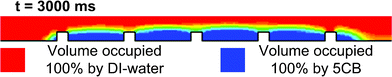
Fig. 4 shows the distribution of DI-water and 5CB in the channel at different time instants, with an infusing water flow speed of 8 mm s−1 (i.e. volumetric flow velocity 400 μL min−1, according to the dimension of the channel). The speed of the DI-water stream was then decreased to 0 abruptly after 2000 ms. The DI-water formed a “plug” flow which pushes away 5CB inside the channel. However, with the protection of Ni grids, a thin layer of 5CB liquid crystal was left, and the thickness of the layer was about 30 μm, the same as the thickness of the Ni grids. As shown in Fig. 5, a figure of the 5CB/DI-water distribution near the Ni-grid area after 3000 ms depicts the simulated quasi-static status of the 5CB thin layer. Judging from the uniformity of the LC thin film, the operation time, and the stability of the thin film over the simulation time, this control profile (flow velocity: 400 μL min−1 for 2000 ms for “cutting” then 0 for 1000 ms to let the remaining LC settle) was an optimized solution, thus was used for subsequent experiments with adaptation to the dimensions of the real devices.
 | ||
| Fig. 4 Distribution of DI-water and 5CB in the channel at different time instants, calculated from a volume of fluid (VOF) model. The distribution of DI-water and 5CB is represented by their “volume fraction” (i.e. the volume ratio of DI-water or 5CB to the total volume). The blow-up figures on the right depict the DI-water/5CB interface near the Ni grids. (a) At 25 ms, DI-water continues to flow into the channel at a velocity of 8 mm s−1. (b) After 100 ms, the 5CB above the Ni grids is already pushed away by the water flow (i.e. the “cutting” process). (c) After 500 ms, DI-water reaches the outlet of the channel. (d) After 2000 ms of continuous water flow, only a thin layer of 5 CB is left near the region of Ni grids. | ||
 | ||
| Fig. 5 The interface between DI-water and 5CB at quasi-static state after the cutting process. The volume fractions of both liquids show an abrupt change at the interface (different colours corresponding to different volume fractions). | ||
Results and discussion
Creating LC thin film using laminar flow and sensing test with DTAB surfactant
Since the orientations of thermotropic LCs in contact with water are sensitive to the types and concentrations of surfactants present in the aqueous phase,15 a simple yet effective way to preliminarily test the sensing performance of our devices is to firstly form the LC thin film by DI-water cutting, then introduce surfactant solution into the microchannel and observe the interaction at the LC-aqueous interface. For easy preparation without losing generality, we chose DTAB (10 mM in DI-water) as our analyte for the sensing test.15Fig. 6 and Fig. 7 show the process of DTAB surfactant detection by our sensing devices with the gold/SAM coating and the DMOAP coating, respectively. For both devices, LC was first introduced by one of the syringe pumps and filled the Ni supporting grid as well as the rest of the space in the sensing channel. The thickness of LC in the sensing channel was ∼250 μm, through which the orientation of the LC mesogens could not be communicated. The LC mesogens, therefore, resumed a non-homeotropic orientational profile through the thickness of the sensing channel, which resulted in birefringence through the thickness of the LC film. Bright images of the 5CB in the grid structure, as shown in Fig. 6(a) and Fig. 7(a), were obtained under the cross-polar observation with the POM.
 | ||
| Fig. 6 POM images of the sensing process for 10 mM DTAB surfactant with a gold/SAM coated device. (a) The sensing channel was filled with LC; (b) the sensing channel was flushed with DI-water, a LC thin film was created within the Ni grid structure at the bottom of the channel; (c) surfactant solution was introduced into the channel. The LC thin film responded to the surfactant and resumed a homeotropic alignment profile. Scale bar: 1 mm. | ||
 | ||
| Fig. 7 POM images of the sensing process for 10 mM DTAB surfactant with a DMOAP coated device. (a) The sensing channel was filled with LC; (b) the sensing channel was flushed with DI-water, a LC thin film was created within the Ni grid structure at the bottom of the channel; (c) surfactant solution was introduced into the channel. Scale bar: 1 mm. | ||
DI-water was then subsequently introduced into the sensing channel at a high flow rate of 400 μL min−1, which corresponded to a linear velocity of 8 mm s−1, given the dimension of the channel. As expected in previous simulation, this laminar flow cut and pushed away the 5CB above the grid structure, leaving only 5CB thin films supported by the grid. The resultant 5CB thin films possessed approximately the same thickness of the grid structure (∼30 μm). A horizontal LC-aqueous interface was thus automatically formed on top of the hexagonal cells. Because the bottom surfaces of the sensing channels were functionalized with mixed alkanethiol SAM or DMOAP, 5CB molecules at the bottom of the thin films were anchored homeotropically, i.e. perpendicular to the surface. At the same time, the orientation of the LC at the top surface of the thin films depends on the property of the contacting target phase or the analytes in that phase. The 5CB mesogens at the top surface possess planar alignment upon contact with DI-water. Therefore, a bend and splay deformation was formed in the 5CB thin film, i.e. from the homeotropic alignment at the bottom to the planar alignment at the top.14 Under the cross-polar observation, 5CB thin film in the grid appeared bright and colourful, as shown in Fig. 6(b) and Fig. 7(b). A comparison of Fig. 6(b) with 6(a) reveals that the interference colours in Fig. 6(b) are lower order, consistent with a decrease in LC film thickness. In addition, within Fig. 6(b), the interference colours are consistent within the sample, indicating formation of a uniform film.
When 10 mM DTAB surfactant solution was introduced into the sensing channel, the 5CB molecules at the top surface assumed a homeotropic alignment, i.e. perpendicular with the LC-aqueous interface. The LC thin film thus had a uniform vertical molecular alignment profile through the thickness. Under this condition, the LC thin film does not possess optical birefringence. As a result, a dark image as shown in Fig. 6(c) and Fig. 7(c) was obtained under cross-polar observation.
There are various methods to quantitatively evaluate the optical signals generated by the LC, for example, using an avalanche photodiode array to detect and measure the intensity of light coming out of each region of LC. Here, we analyzed the images of each cell in the device and calculated the intensity of light transmitted through crossed polarizers, quantified as the average luminance of the images, utilizing ImageJ (Open source image analysis software developed at the National Institutes of Health). The resulting average luminance of the LC region in Fig. 7(b) was 120, while in Fig. 7(c) , the average luminance was less than 30.
Characterizing interaction between phospholipase (PLA2) and phospholipids (L-DLPC)
Phospholipase A2 hydrolyzes L-phospholipids to form fatty acid and lysophospholipid products. Phospholipases are involved in inflammatory responses and thus are widely investigated in a range of basic biological and medicinal contexts.26–28 The characterization of phospholipase activity using a phospholipid monolayer self-assembled at the aqueous–LC interface was demonstrated to be an effective method of reporting the activity of PLA2.15 The orientation of LCs is coupled to the presence of phospholipids, thus the enzymatic events occurring on the phospholipids can be clearly characterized by examine the optical property of the LCs. Thus, our LC thin film devices are expected to be an effective real-time label-free method for sensing/characterizing the PLA2 binding/hydrolyzing event. The sensing results utilizing the gold/SAM coated device was described in detail, while the DMOAP coated device gave a similar performance, as shown in Fig. 11.Creating lipid-decorated LC-aqueous interfaces
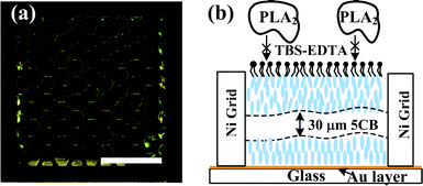
To form a lipid monolayer at the aqueous-5CB interface, an aqueous dispersions of L-DLPC was used to conduct the LC pushing and cutting process. Similar with the cutting and pushing process with the DTAB aqueous surfactant solution, the laminar flow of aqueous dispersion of L-DLPC vesicles, at the flow rate of 400 μL min−1 (8 mm s−1), was introduced into the sensing channel by a syringe pump and formed 5CB thin films contained in the Ni grid. When the 5CB thin films were initially formed, the optical texture was bright (Fig. 8(a)), indicating the planar orientation of the 5CB mesogens at the LC–aqueous interface. The tilted angle of 5CB mesogens relative to the surface normal decrease linearly through the 5CB thin film from nearly 90° (to the vertical direction) at the 5CB–aqueous interface to 0° at the mix alkanethiol SAM–5CB interface on the substrate surface. The bending and splay distortions in the 5CB thin film resulted in a continuous variation of the mesogen orientation through the thickness, as shown in Fig. 8(d), which resulted in a birefringence (∼0.09) in the 5CB thin film. This led to a yellow/green/pink appearance under cross-polar observation. After 5CB thin film was formed in the whole grid structure, the phospholipid solution in the sensing channel was set to be static (flow velocity = 0). As time evolved, due to the interaction between the lipid and the 5CB mesogens, homeotropic anchoring of 5CB at the aqueous–5CB interface was achieved, as shown in Fig. 8(e). Given the homeotropic alignment of mesogens at the mix alkanethiol SAM–5CB interface at the bottom of the LC film, the 5CB mesogen orientational alignment profile through the film was undistorted. Towards the end of the equilibration period, dark and uniform optical texture was observed, as shown in Fig. 8(c). This implied that a monolayer of L-DLPC lipids was formed at the aqueous–5CB interface. For following sensing of PLA2 binding, lipid-free buffer solution (TBS) was introduced into the sensing channel at a flow rate of 20 μL min−1, flushing away unabsorbed phospholipids. | ||
| Fig. 8 Process of creating lipid-decorated LC-aqueous interface with a gold/SAM coated sensing device. LC thin film was formed in the grid structure by cutting with an aqueous dispersion of L-DLPC vesicles, similar to the process described above (flow rate: 8 mm s−1). (a)(d) The freshly-formed thin film demonstrated birefringence upon cutting. (b) 10 min after the cutting DLPC solution was set to be steady. (c)(e) Over a period time of 20 min, monolayer of DLPC was formed at the LC–aqueous interface. LC molecules coupled with the phospholipid at the interface and resumed homeotropic orientation. With cross-polar observation, the bright and colourful image of LC thin film evolved to a dark image. When the interface was formed, TBS buffer solution slowly flew across the lipid-laden interface for ten minutes rinsing away remaining phospholipid, as shown in the last image (flow rate: 0.3 mm s−1). Scale bar: 1 mm. | ||
Detecting PLA2 enzymatic activity
The presence of Ca2+ is needed for PLA2 to be functional. The active site of PLA2 binds Ca2+, which in turn facilitates PLA2 to recognize the sn-2 acyl bond of L-phospholipids and catalytically hydrolyze the phospholipids, forming single-tailed lysophospholipids and fatty acids.25 Once formed, the products either phase-separate from the phospholipids or desorb from the interface, thus disrupting the anchoring of the LC.In our experiment, as a control we first introduced 100 nM PLA2 solution without Ca2+ after the formation of the L-DLPC monolayer at the aqueous–5CB interface. The dark appearance of the 5CB thin film did not change even 40 min after introducing PLA2 solution without Ca2+. This indicated that the binding event of PLA2 with the L-DLPC did not take place and the 5CB mesogens remained homeotropic alignment at the interface, consistent with previous study (Fig. 9).25
 | ||
| Fig. 9 PLA2 solution without Ca2+ was introduced into the microfluidic channel by an external syringe pump. The orientation of the LC molecules in the grid structure did not change even after 40 min of exposure to the solution, and under cross-polar observation, the LC remained dark. Scale bar: 1 mm. | ||
A 100 nM PLA2 solution with Ca2+ (also 100 nM) was then introduced into the sensing channel at a flow rate of 0.4 mm s−1. The 5CB thin film in the grids at the centre of the sensing channel started to change the appearance to a colour and bright image. This indicated that, with the presence of Ca2+, specific binding of PLA2 to the monolayer of 5CB supported at the aqueous–5CB interface and subsequent hydrolysis of the monolayer took place. In a period of 30 min, this optical texture appearance transit started from the grids close to the center of the channel and spread towards the two sides of the width of the sensing channel, as shown in Fig. 10 (a)–(c). This optical texture appearance transit indicated that the PLA2 bound with and hydrolyzed the monolayer of L-phospholipid, which triggered the orientational transition of 5CB to a planar alignment, as shown in Fig. 10(d).
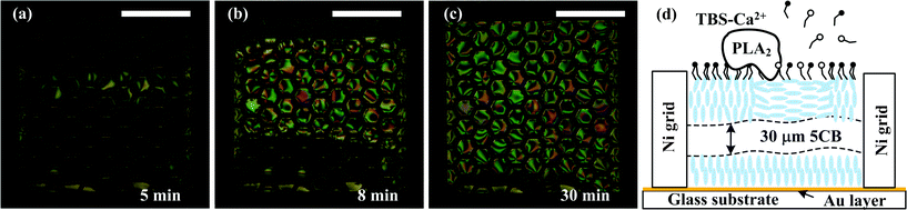 | ||
| Fig. 10 100 nM PLA2 solution in TBS-Ca2+ was introduced into the sensing microchannel by an external syringe pump at a flow rate of 20 μL min−1 (0.4 mm s−1). Interaction between PLA2 and the monolayer of DLPC induced orientational transition of the 5CB mesogens, resulting in a gradual change of the appearance of the LC grids from dark to bright and colourful. The whole process took ∼30 min. Scale bar: 1 mm. | ||
Characterizing interaction between PLA2 and L-DLPC with a DMOAP-coated device
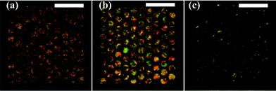
Experimental procedures similar to that described above were employed to demonstrate the capability of the DMOAP-coated device for sensing the PLA2 binding/hydrolyzing event, as shown in Fig. 11. Fig. 11(a) shows the POM image of the LC thin film right after cutting by the aqueous dispersions of L-DLPC. The L-DLPC dispersions were then set steady. The birefringence began to disappear in 2 min and the thin film turned almost completely dark under cross-polar observation (Fig. 11(b)). Without Ca2+, PLA2 was not be able to bind and hydrolyze L-DLPC, thus the POM image remained dark after 40 min since the LC thin film exposed to 100 nM PLA2 solution without Ca2+ (Fig. 11(c)). However, after introducing Ca2+ (100 nM), PLA2 began to catalytically hydrolyze L-DLPC and thus the LC thin film in most of the hexagonal cells under cross-polar observation turned to bright and colourful in 30 min (Fig. 11(d)). | ||
| Fig. 11 Sensing PLA2 binding/hydrolyzing event using a DMOAP-coated device. (a) The LC thin film immediately after cutting by the L-DLPC dispersion (flow rate: 8 mm s−1). (b) 20 min after the cutting. (c) 40 min after introducing the PLA2 solution without Ca2+ (flow rate: 0.4 mm s−1). (d) 30 min after introducing the 100 nM PLA2 solution with Ca2+ (flow rate: 0.4 mm s−1). Scale bar: 1 mm. | ||
Repeatability test
The repeatability of the devices was tested. In this test, DTAB solution was used to form the LC thin film as well as to modulate the LC mesogen alignments. In the first round experiment, LC film was formed by the laminar flow of DTAB solution and stabilized to demonstrate homeotropic alignment as described above. The colour of the film under cross-polar observation changes from bright to dark. Then the sensing channel was purged using ethanol so that DTAB solution as well LC thin film was removed from the channel. N2 stream was then applied to dry the channel for 30 min. LC was again introduced into the channel and filled the hexagonal Ni container at the bottom. DTAB solution was introduced into the channel and for the second time formed the LC thin film. The experiment was repeated twice, and similar qualities of LC thin films and LC mesogen alignments were achieved. For each cutting process, it was observed that only less than 5% LC cells in the device did not correctly fill after the cutting process. The lifetime of the device, i.e. the time of the LC film remains stable and active, was not optimized in these experiments, but we observed it to be more than 48 h. This was determined by forming the LC film with DI water, storing the device for 36 h, and then using the device to performing sensing tests (as described above). More results addressing the repeatability of the experiments are available in the ESI.†Conclusions
We have demonstrated microfluidic devices which integrated thermotropic LC sensing into microfluidic channels. The fluidic dynamic phenomenon in the laminar flow regime was investigated and employed to create a layer of LC thin film in an in situ fashion, which greatly improved the efficiency of preparing the delicate LC sensing element and eliminated the complicated and skill-required manual handling. The subsequent sensing tasks thus can be conducted in situ, and remotely controlled by lab-on-a-chip control methods. As a result, the devices inherit the high sensitivity, real-time sensing and label-free detection properties from LC sensing, and meanwhile possess the capability to conduct multiple consecutive sensing tasks, as well as the detecting tasks in the hazardous environment inaccessible to human being. Two model systems were demonstrated on the sensing devices. The alternative flow of the aqueous dispersion of DTAB surfactant and DI-water was detected by the orientational transits of the LC mesogens and reflected as the real time change of the LC optical texture. LC optical texture change also effectively indicated the spontaneously assembling of the L-DLPC phospholipid monolayer at the LC interface and subsequently, the binding/hydrolyzing event of PLA2 in the sensing channel with this phospholipid monolayer. In future studies, we will focus on using photon detectors to quantify the intensity of the light transmitted through the LC and polarizers, and investigate in detail the sensitivity and reliability of our system for a variety of chemical systems.Acknowledgements
This research was supported by the U.S. National Science Foundation (Grant number: ECCS 0622202). N. L. Abbott received partial support from the NSF MRSEC program (DMR-1121288), the ARO (W911-NF-11-1-0251), and the NIH (CA108467 and AI092004) for this research. This research utilized NSF-supported shared facilities at the University of Wisconsin. The authors would like to thank J. S. Lee, B. S. Aldalali, and G. M. Koenig, Jr. for technical assistance and Dr K. D. Caldwell for helpful discussions.References
- R. S. Muller and IEEE Electron Devices Society, Microsensors, New York: IEEE Press, 1991 Search PubMed.
- B. H. Timmer, K. M. van Delft, W. W. Koelmans, W. Olthuis and A. van den Berg, IEEE Sens. J., 2006, 6, 829–835 CrossRef CAS.
- R. R. Shah and N. L. Abbott, Science, 2001, 293, 1296–1299 CrossRef CAS.
- K.L. Yang, K. Cadwell and N.L. Abbott, Sens. Actuators, B, 2005, 104, 50–56 CrossRef.
- S. S. Sridharamurthy, K. D. Cadwell, N. L. Abbott and H. Jiang, Smart Materials and Structures, 2008, 17 Search PubMed.
- R. R. Shah and N. L. Abbott, J. Am. Chem. Soc., 1999, 121, 11300–11310 CrossRef CAS.
- J. J. Skaife, J. M. Brake and N. L. Abbott, Langmuir, 2001, 17, 5448–5457 CrossRef CAS.
- J. M. Brake, M. K. Daschner, Y. Y. Luk and N. L. Abbott, Science, 2003, 302, 2094–2097 CrossRef CAS.
- J. S. Park, S. Teren, W. H. Tepp, D. J. Beebe, E. A. Johnson and N. L. Abbott, Chem. Mater., 2006, 18, 6147–6151 CrossRef CAS.
- K. L. Yang, K. Cadwell and N. L. Abbott, J. Phys. Chem. B, 2004, 108, 20180–20186 CrossRef CAS.
- T. L. Yang, S. Y. Jung, H. B. Mao and P. S. Cremer, Anal. Chem., 2001, 73, 165–169 CrossRef CAS.
- M. L. Kinsinger, B. Sun, N. L. Abbott and D. M. Lynn, Adv. Mater., 2007, 19, 4208–4212 CrossRef CAS.
- D. Cheng, I. H. Lin, N. L. Abbott and H. Jiang, IEEE Transducers, Denver, CO, USA, June 21–25, 2009 Search PubMed.
- J. M. Brake and N. L. Abbott, Langmuir, 2002, 18, 6101–6109 CrossRef CAS.
- J. M. Brake, A. D. Mezera and N. L. Abbott, Langmuir, 2003, 19, 6436–6442 CrossRef CAS.
- J. M. Brake and N. L. Abbott, Langmuir, 2007, 23, 8497–8507 CrossRef CAS.
- V. K. Gupta and N. L. Abbott, Phys. Rev. E: Stat. Phys., Plasmas, Fluids, Relat. Interdiscip. Top., 1996, 54, R4540–4543 CrossRef CAS.
- R. A. Drawhorn and N. L. Abbott, J. Phys. Chem., 1995, 99, 16511–16515 CrossRef CAS.
- T. Rasing and I. Muševič, Surfaces and Interfaces of Liquid Crystals, Springer, 2004 Search PubMed.
- X. Bi, S. Huang, D. Hartono and K. Yang, Sens. Actuators, B, 2007, 127, 406–413 CrossRef.
- S. Noonan, A. Shavit, B. R. Acharya and D. K. Schwartz, ACS Appl. Mater. Interfaces, 2011, 3, 4374–4380 Search PubMed.
- F. J. Kahn, Appl. Phys. Lett., 1973, 22, 386–388 CrossRef CAS.
- J.-W. Kim, H. Kim, M. Lee and J. J. Magda, Langmuir, 2004, 20, 8110–8113 CrossRef CAS.
- Z. Yang and N. L. Abbott, Langmuir, 2010, 26, 13797–13804 CrossRef CAS.
- A. G. Chmielewski and E. Lepakiewicz, Rheol. Acta, 1984, 23, 207–210 CrossRef CAS.
- E. A. Dennis, the Journal of Biological Chemistry, 1994, 269, 13057–13060 CAS.
- J. P. Nicolas, Y. Lin, G. Lambeau, F. Ghomashchi, M. Lazdunski and M. H. Gelb, J. Biol. Chem., 1997, 272, 7173–7181 CrossRef CAS.
- A. Argiolas and J.J. Pisano, the Journal of Biological Chemistry, 1983, 258, 13697–13702 CAS.
Footnotes |
| † Published as part of a theme issue on optofluidics |
| ‡ Electronic supplementary information (ESI) available: See DOI: 10.1039/c2lc40462a/ |
| This journal is © The Royal Society of Chemistry 2012 |