Three dimensional nickel–graphene core–shell electrodes†
Xiaoyin
Xiao
a,
Joseph R.
Michael
a,
Thomas
Beechem
a,
Anthony
McDonald
a,
Mark
Rodriguez
a,
Michael T.
Brumbach
a,
Timothy N.
Lambert
a,
Cody M.
Washburn
a,
Joseph
Wang
b,
Susan M.
Brozik
a,
David R.
Wheeler
a,
D. Bruce
Burckel
*a and
Ronen
Polsky
*a
aSandia National Laboratories, Albuquerque, New Mexico 87185, USA
bDepartment of NanoEngineering, University of California at San Diego, La Jolla, California 92093-0448, USA
First published on 12th September 2012
Abstract
The annealing of nickel-coated porous carbon structures results in a new three dimensional nanostructured graphene encapsulated nickel core–shell electrode. A highly interdependent and dynamic process is observed that results in the complete reversal of the spatial orientations of the two component system after the annealing process. We examine the mechanism of carbon diffusion and observe unexpected morphological changes of the nickel in response to carbon crystallization. The new nickel–graphene core–shell electrode demonstrates excellent electrochemical properties with promising applications in micro-batteries and biosensors.
The unique electronic and optical properties of graphene have inspired considerable research interest since the discovery of a method to isolate monolayer graphene in 2004.1,2 The fabrication of three dimensional (3D) graphene structures has been published recently based on chemically derived macroporous nickel foam substrates that have different electrical, mechanical, and thermal properties over planar 2D graphene.3–5 This manuscript details the fabrication of a new 3D graphene material, a nanoscale nickel–graphene core–shell structure. In addition to electrochemical applications put forth here, insight into the more general processes of carbon diffusion through bulk nickel is examined with unexpected morphological changes of the nickel catalyst being observed related to the crystallization of the carbon into graphene.
Elemental carbon can bond to itself in either sp2 or sp3 hybrid orbitals. In crystalline form these create graphitic allotropes such as fullerene/carbon nanotubes (sp2) or diamond (sp3) which can exhibit remarkably disparate physical properties.6 Glassy carbon, formed when carbon-rich organic material is heated in a reducing atmosphere, exists as an amorphous admixture of both sp2 and sp3 bonded carbon atoms. As a subset of glassy carbon, pyrolyzed photoresist films (PPF) are capable of creating 2D and 3D carbon structures by heating lithographically patterned organic photoresist films in flowing forming gas.7–9 Although the ratio of sp2 to sp3 bonded carbon in PPF films can be adjusted slightly depending on photoresist choice and annealing conditions, the carbon exists predominately as amorphous sp3 rather than sp2 carbon.
Numerous carbon sources can be made into graphene following Ni coating and annealing.10 Recently, we reported the fabrication of 3D graphene structures prepared by the annealing of Ni sputter-coated porous PPF patterned by interferometric lithography.11 These 3D monolithic structures were shown to contain two domains of multilayered graphene; one region of less than 5 monolayers of graphene on the interconnecting arms and one region of greater than 10 layers of graphene at the three-fold interstitial nodes. After acidic etching of the nickel the 3D graphene was shown to be hollow and exhibited excellent electron transfer properties for use in electrochemical applications. The structures before acidic etching reveal nickel encapsulated graphene 3D electrodes that exhibit electrochemical properties different from the hollow core–shell 3D graphene structures. We also explore the unique process and possible mechanism for diffusion and ordering of the carbon into few-layer graphene.
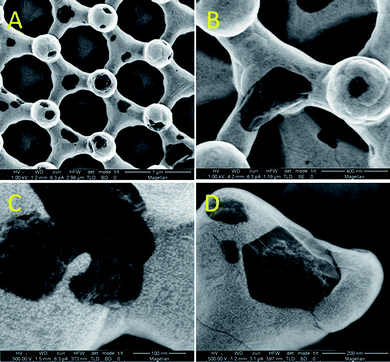
The formation of the lithographically defined 3D carbon scaffolds is outlined in detail elsewhere.12 Briefly, three separate exposures of a two-beam interferometric lithography pattern were used to create a nominally face centered cubic lattice in photoresist. The pattern was then pyrolyzed in a tube furnace with flowing forming gas, yielding a 3D carbon scaffold with predominately amorphous sp3 carbon. After pyrolysis, the films were placed in a standard sputtering chamber where nickel was sputtered at a rate of ∼0.7 Å s−1 for 2600 seconds to create a nominally conformal nickel shell around the carbon. Fig. 1A shows the SEM of the pre-converted porous pyrolyzed photoresist film electrode while Fig. 1B shows the structures after Ni sputtering. X-ray diffraction (XRD) indicates the existence of small 13 nm Ni crystallites after the sputtering process, based on the Ni peak full width half maximum (FWHM), and that the carbon is in an amorphous state, shown in Fig. 2 (black curve). Following graphene conversion through a rapid thermal annealing process (750 °C for 20 min in forming gas at 1 Torr) the structures appear indistinguishable from the hollow 3D graphene reported previously10 as shown in Fig. 1C; however increasing the accelerating voltage used in the SEM from 1 to 15 kV (Fig. 1C–E) results in an increased depth of sampling that begins to reveal sub-surface information. The increased accelerating voltage allows backscattered electron images to be obtained where the higher intensity regions reveal an internal interconnected network, Fig. 1F. This backscattered electron image indicates the structures are filled with a higher atomic number material with a higher backscattered electron yield. Remarkably the inner amorphous carbon has graphitized outside of the nickel while the original nickel coating is now completely encapsulated inside the new graphene shell as a solid core.
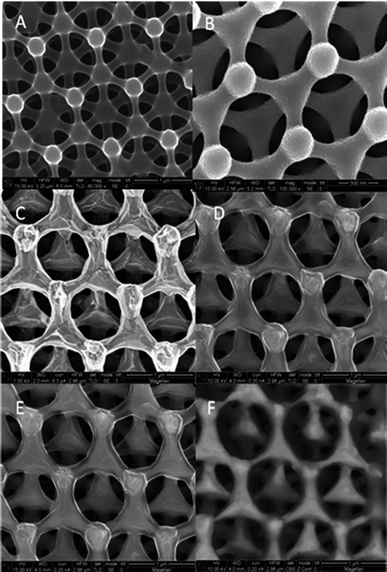 | ||
| Fig. 1 SEM micrographs of porous carbon (A), secondary electron image of nickel-coated porous carbon (B), secondary electron image after annealing at 750 °C for 20 min in forming gas and imaged at 1, 10, and 15 kV SEM accelerating voltage (C–E), and backscattered electron image (F). | ||
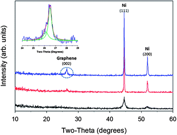 | ||
| Fig. 2 X-Ray diffraction measurements of nickel-coated amorphous carbon (black curve), partially graphitized 3D carbon structure (red curve), and fully formed nickel encapsulated graphene 3D core–shell electrode (blue curve). Inset: longer scan of graphite (002) peak. | ||
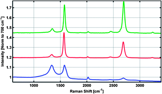
Raman spectroscopy was used to assess the quality of the carbon material. Shown in Fig. 3 are two representative spectra in which the characteristic D (1350 cm−1), G (1600 cm−1) and 2D (2700 cm−1) bands of graphitic material are observed (green and red curves). The resulting shell of graphitic carbon shows a relatively high degree of order as indicated by the relatively small D to G-band intensity ratio. Additionally, the relatively pronounced 2D to G intensity ratio in certain locations indicates the presence of multilayered graphene similar to our previous report in which the Ni was completely removed.10 Notably reduced is the broadband photoluminescence typically observed when imaging few layer graphene atop a metal with a visible wavelength source. XRD measurements, Fig. 2 (blue curve), indicate the presence of both graphite and metallic nickel (with approximately ∼18![[thin space (1/6-em)]](https://www.rsc.org/images/entities/char_2009.gif) :82 weight percent respectively). A slight peak shift is observed for the graphite (002) to a lower angle which suggests a slight expansion of the graphitic layering. The broad nature of the graphite (002) peak could suggest some strain presence within this phase. A longer scan of the graphite (002) peak suggests two possible dimensions of the graphite layering, Fig. 2: inset. The derived c-axis length based on profile fitting of the (002) doublet peak yields a value of ∼6.74 Å and 6.82 Å. These values are larger than the 6.72 Å c-axis of highly ordered pyrolytic graphite (HOPG) lattice.
:82 weight percent respectively). A slight peak shift is observed for the graphite (002) to a lower angle which suggests a slight expansion of the graphitic layering. The broad nature of the graphite (002) peak could suggest some strain presence within this phase. A longer scan of the graphite (002) peak suggests two possible dimensions of the graphite layering, Fig. 2: inset. The derived c-axis length based on profile fitting of the (002) doublet peak yields a value of ∼6.74 Å and 6.82 Å. These values are larger than the 6.72 Å c-axis of highly ordered pyrolytic graphite (HOPG) lattice.
 | ||
| Fig. 3 Representative Raman spectra for 3D nickel–graphene core–shell electrode (red, green) and partially graphitized samples (blue). | ||
X-ray photoelectron spectroscopy (XPS) measurements, shown in Fig. S1,† show a C1s peak that is identical to HOPG, indicating a better than 99% conversion from sp3 to sp2 carbon, and <1% total mass due to Ni. The probing depth of the XPS is on the order of a few nanometers and does not indicate any substantial amount of Ni on the exterior of the structures, while the XRD and SEM indicates a large Ni presence and an inner metallic core respectively (shown in Fig. S2†); this is further confirmation that the two materials are spatially separated and have completely switched original orientations. SEM cross sections shown in Fig. 4A show multiple areas where Ni is protruding from broken graphene arms (yellow arrows) and back scattered imaging in Fig. 4B show that this Ni interior pervades throughout the structures. Particularly striking is the inner Ni core that exists inside the large domed nodes when comparing the two figures (red arrows) also shown in cross-section in Fig. 4C. If the original carbon structure had simply diffused and graphitized outside of the Ni then one would not have expected a solid Ni core as seen here. This suggests that the Ni shell has undergone a significant rearrangement itself.
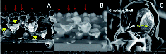 | ||
| Fig. 4 Cross-section secondary electron SEM micrographs of 3D nickel–graphene core–shell structures (A) and (C) and backscattered electron image (B). Yellow arrows indicate where Ni is protruding from broken graphene arms and red arrows indicate large domed nodes. | ||
The formation of graphene on transition metal catalysts using precipitation techniques such as chemical vapor deposition (CVD) have been widely studied,13–15 however the exact mechanism responsible for graphene nucleation and growth is still the subject of much discussion. No detailed explanation has been put forth on the mechanism for graphene formation used in the method described here; annealing a sacrificial carbon source that has been coated with a nickel layer, yet it is reasonable to assume that there should be some similarities which we now discuss further. It is generally accepted that the nucleation and growth of graphene on transition metal catalysts proceeds by two basic steps (i) diffusion of carbon atoms into the metal upon heating and (ii) crystallization (graphitization) of the carbon upon cooling. Transition metals catalysts such as Ni and Ru are known to produce thicker multilayer graphene films than Cu (for instance) due to the higher solubility of carbon.
In order to shed light on the graphitization process, the annealing conditions were altered to study the sample just at the onset of graphitization. Pressure is known to influence the formation of graphene on transition metal catalysts affecting the timescale of the carbon precipitation/crystallization process.16,17 Therefore we annealed our samples at atmospheric pressure for the same time period and temperature which resulted in an intermediate stage in graphene conversion. SEM pictures presented in Fig. 5 show small patches of carbon (10 to 100's of nm) on the Ni surface. The graphene islands appear to be slightly embedded within the Ni framework. The carbon source in this method must diffuse up through grain boundaries and therefore does not necessarily crystallize directly on top of the Ni surface as is seen with precipitation techniques. Focused ion beam cross-sectional imaging (Fig. S3†) show that many of the graphene islands are surface bound and separated from the inner carbon core by the Ni shell. This is the intermediate stage of the reversed spatial orientation of the carbon and Ni. Raman analysis shows that this structure consists of a disordered carbon layer as shown in Fig. 3 (blue curve). In this layer, the large I(D) to I(G) ratio and concomitant reduction in the 2D mode intensity suggest that the carbon material is nanocrystalline. The larger Ni background relative to the carbon source coupled to an overall weaker signal indicates a thinner graphene layer at this stage of growth as would be expected. XRD, Fig. 2 (red curve), shows a small crystallite graphite peak and considerably sharper (FWHM) Ni peaks suggesting Ni grain growth and recrystallization compared with the sputtered, pre-annealed sample in Fig. 1B. The estimated crystallite size for Ni exceeds 100 nm which is the instrumental limit in this case. Large Ni grains can clearly be visualized in the SEM images presented in Fig. 5.
 | ||
| Fig. 5 Secondary electron SEM micrographs of partially graphitized electrodes. | ||
There has been much evidence that graphene nucleation occurs predominately at Ni (111).18–20 Recent reports however have indicated that this is not just a surface process and that sub-surface interactions are an important and not yet elucidated factor in graphene formation.16,21 The growth of graphene across step edges on Ru has been shown to etch Ru such that the underlying metal terrace grows together with the graphene.22 This leads to a transformational occurrence in the Ru structure where Ru atoms will transport themselves to increase the size of a crystal plane for graphene to grow on. This has not been observed on Ni, however Li et al. have recently reported on modeling simulations which indicate that Ni (111) does not play a passive role in graphene nucleation but rather rearranges itself showing great mobility during graphene formation as carbon migrates from sub-surface Ni (111) to neighboring Ni (111) interstitial sites.23 A dynamic response at grain boundaries such that new Ni (111) step edges are formed after nucleation could explain how the Ni exterior ends up as a solid core in our structures. An overlapping of the graphene islands along with the bulk of the carbon diffusing through grain boundaries is the second part of this process which completes the formation of the shell and also leads to the multilayering of the graphene. The most likely scenario for the multilayer growth is new graphene sheets nucleating under existing sheets at the carbon–Ni interface rather than on top of the shell.24 The high level of faceting observed indicates that many of the graphene islands grow from single crystals,25,26 as can be observed in Fig. 5C and D. The growth of many individual crystals inherently produce numerous edge defects ultimately responsible for its efficacious electron transfer properties.27
The combination of highly conductive multilayered graphene with electrochemically active Ni results in an electrode with different properties from the hollow 3D porous graphene monoliths. The cyclic voltammetric response of the electrode in 0.5 M NaOH shown in Fig. 6A exhibits redox peaks due to electrochemically cycling between Ni(OH)2 and NiOOH. Despite being encapsulated inside the graphene shell these results indicate that solution can still access the inner nickel core, presumably through shell defects, shell expansion, or pin holes. The low ΔEp of ∼80 mV demonstrate favorable electron transfer kinetics occurring. The current response increases up to 500 cycles due to enlarging of surface defects from volume changes associated with repeated formation/reduction of nickel intermediates. It is worth noting here that the inner Ni core is not consistent throughout the bulk of the electrode and many hollow voids within the 3D structure are observed (Fig. S4†). A possible application of such 3D porous core–shell structures is non-enzymatic glucose detection. Nickel is well known to have high electrochemical activity towards glucose oxidation in alkaline media, unlike carbon which exhibits minimal catalytic activity towards glucose. Cyclic voltammograms of glucose oxidation in 0.5 M NaOH are shown in Fig. 6B. It is clear that glucose oxidation is significantly catalyzed by Ni catalysts up to 400 μA cm−2 per mM concentration and a linear relationship is observed in the physiological range of glucose concentration (1–10 mM). No such catalytic activity was observed when the structures were only graphene after Ni etching (data not shown). The large catalytic current is partially attributed to the enhanced mass transport at the 3D porous substrates from the nanometer scale dimensions.28 When increasing the scan rate (5, 50, and 500 mV s−1), the negative current at the reverse scan starts to appear and the normalized current decreases, indicating that glucose oxidation is limited by glucose diffusion, not by the redox process of Ni (Fig. 6C). Ni oxidation at positive potentials can create highly resistive oxide layers, which is not observed here. Fig. 6D clearly indicates that the catalytic glucose oxidation reaches steady-state current much faster than that at the sputtered Ni film before rapid thermal annealing. The lower current is most likely due to the lack of accessibility to the encapsulated Ni as opposed to the larger volume of Ni present on the sputter-coated carbon. However the improved kinetics observed on the Ni-encapsulated graphene electrode makes it much more attractive for fast amperometric glucose sensing.
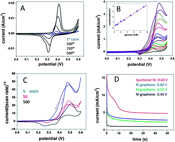 | ||
| Fig. 6 Cyclic voltammograms of graphene/Ni electrodes in (A) 0.5 M NaOH, increasing concentrations of glucose (B), 8 mM of glucose at 5, 50, and 500 mV s−1 (current normalized to scan rate). Chronoamperometric curves of 8 mM glucose comparing sputtered nickel porous carbon and graphene/nickel electrodes at various potentials. | ||
In summary, the three dimensional highly interconnected nature of porous carbon fabricated by interferometric lithography has provided a unique platform to study the carbon crystallization process where the resulting structures consist of a multilayered graphene shell encapsulating a solid nickel core. The diffusion and crystallization of carbon from an inner amorphous carbon core with an exterior Ni transition metal catalyst results in the reversed spatial orientation of the two components suggesting a dynamic interdependent growth process. The new nanostructured graphene/nickel core–shell electrodes have possible applications in micro-batteries and biosensors.
Experimental
Scanning electron microscope (SEM) imaging was performed on a Zeiss Supra 55VP field emission gun scanning electron microscope or an FEI Magellan 400 SEM. XRD data were obtained using a Siemens q–2q D500 diffractometer equipped with a sealed tube X-ray source (Cu anode, l = 1.5406 Å), a diffracted beam graphite monochromator and a scintillation detector. Fixed incident and diffracted beam slits (1° aperture) were employed (goniometer radius 200 mm). Data were collected over an angular range of 5–80° 2q with a step-size of 0.04° 2q and a count time of 4 seconds per step using Bragg–Brentano geometry.Interferometric lithography of 3D porous carbon electrodes. A bottom anti-reflection coating (BARC), iCON-7 (Brewer Science, Rolla Missouri) was spun onto Silicon wafers at 3000 RPM and baked on a vacuum hotplate at 205 °C for 60 s. Negative tone NR7 from Futurrex Inc. was used in all of the experiments. A thin layer of NR7-100P (∼100 nm) was deposited and spun at 3000 RPM to create an adhesion layer. After flood exposure and post exposure bake at 130 °C on a vacuum hotplate, a thick layer (6 μm) of NR7-6000P was deposited and spun at 3000 RPM and soft-baked at 130 °C. The frequency tripled 355 nm line of a Q-switched Nd:YAG laser was used to form the interference pattern. The beam was expanded and split into 2 separate beams and interfered with an angle of 32 degrees between the planewave propagation vectors. The plane of incidence contains both propagation vectors as well as the angle bisector of the propagation vectors, which is tilted with respect to the sample surface normal by 45 degrees. After each exposure the sample is rotated in the plane by 120 degrees and the process is repeated a total of 3 times. After exposure the sample received a post-exposure bake of 85 °C for 2 minutes on the vacuum hotplate. A 120 second puddle development, using RD-6 (Futurrex, Inc.) and spin drying completed fabrication of the resist structures. The samples were baked on a hotplate at 180 °C for 30 minutes. The samples were then pyrolyzed at 1100 °C for 1 hour in forming gas (5% H2 and 95% N2). Substrates were rinsed with isopropanol and water before use.
In order to maintain control over thin film conformity, thickness, and grain size, the Ni sputtering rate was controlled at ∼0.7 Å s−1 by adjusting the distance of the target from the substrate, the chamber pressure, and the DC power supplied to the magnetron. The sputtering time is 2600 s. After Ni sputtering, the substrates were annealed at 750 °C with flow of forming gas (5% H2 and 95% N2) at either ambient or reduced atmosphere. Nonenzymatic glucose detection: the substrates were sliced into ∼1 cm × 4 cm pieces. Each piece was then partially wrapped in the middle using gently melted parafilm, leaving ∼1 cm2 surface area immersed as active electrode surface and the other end to connect to the potentiostat. Electrochemical measurements were performed on a CH Instruments 660 electrochemical analyzer (Austin, TX, USA). All electrochemical experiments were versus a Pt counter and Ag/AgCl in 3 M NaCl reference from Bioanalytical Systems (West Lafayette, IN, USA).
Acknowledgements
Sandia is multiprogram laboratory operated by Sandia Corporation, a Lockheed Martin Company, for the United Stated Department of Energy's National Nuclear Security Administration under Contract DE-AC04-94AL85000. The authors acknowledge the Sandia National Laboratories' Laboratory Directed Research & Development (LDRD)References
- K. S. Novoselov, A. K. Geim, S. V. Morozov, D. Jiang, Y. Zhang, S. V. Dubonos, I. V. Grigorieva and A. A. Firsov, Science, 2004, 306, 666 CrossRef CAS.
- S. Zhengzong, D. K. James and J. M. Tour, J. Phys. Chem. Lett., 2011, 19, 2425 Search PubMed.
- Z. Chen, W. Ren, L. Gao, B. Liu, S. Pei and H. M. Cheng, Nat. Mater., 2011, 10, 424 CrossRef CAS.
- X. Dong, X. Wang, L. Wang, H. Song, H. Zhang, W. Huang and P. Chen, ACS Appl. Mater. Interfaces, 2012, 4, 3129 CAS.
- M. T. Pettes, H. Ji, R. S. Ruoff and L. Shi, Nano Lett., 2012, 12, 2959 CrossRef CAS.
- R. L. McCreery, Chem. Rev., 2008, 108, 2646 CrossRef CAS.
- A. M. Lyons, J. Non-Cryst. Solids, 1985, 70, 99 CrossRef CAS.
- O. J. A. Schueller, S. T. Brittain and G. M. Whitesides, Adv. Mater., 1997, 9, 477 CrossRef CAS.
- S. Ranganathan, R. McCreery, S. M. Majii and M. J. Madou, J. Electrochem. Soc., 2000, 147, 277 CrossRef CAS.
- Z. Yan, Z. Peng, Z. Sun, J. Yao, Y. Zhu, Z. Liu, P. M. Ajayan and J. M. Tour, ACS Nano, 2011, 5, 8187 CrossRef CAS.
- X. Xiao, T. E. Beechem, M. T. Brumbach, T. N. Lambert, D. J. Davis, J. R. Michael, C. M. Washburn, J. Wang, S. M. Brozik, D. R. Wheeler, D. B. Burckel and R. Polsky, ACS Nano, 2012, 6, 3573 CrossRef CAS.
- D. B. Burckel, C. M. Washburn, A. K. Raub, S. R. J. Brueck, D. R. Wheeler, S. M. Brozik and R. Polsky, Small, 2009, 5, 2792 CrossRef CAS.
- C. Mattevi, H. Kim and M. Chhowalla, J. Mater. Chem., 2011, 11, 3324 RSC.
- H. Jiang, Small, 2011, 7, 2413 CAS.
- X. Li, W. Cai, L. Colombo and R. S. Ruoff, Nano Lett., 2009, 9, 4268 CrossRef CAS.
- L. Fan, Z. Li, X. Li, K. Wang, M. Zhong, J. Wei, D. Wu and H. Zhu, Nanoscale, 2011, 3, 4946 RSC.
- X. Li, C. W. Magnuson, A. Venogopa, R. M. Tromp, J. B. Hannon, E. M. Vogel, L. Colombo and R. S. Ruoff, J. Am. Chem. Soc., 2011, 133, 2816 CrossRef CAS.
- R. S. Weatherup, B. C. Bayer, R. Blume, C. Ducati, C. Baehtz, R. Schogl and S. Hofmann, Nano Lett., 2011, 11, 4154 CrossRef CAS.
- L. Baraton, Z. B. He, C. S. Lee, C. S. Cojocaru, M. Chatelet, J. L. Maurice, Y. H. Lee and D. Pribat, Europhys. Lett., 2011, 96, 46003 CrossRef.
- S. J. Chae, F. Gunes, K. K. Kim, E. S. Kim, G. H. Han, S. M. Kim, H. J. Shin, S. M. Yoon, J. Y. Choi, M. H. Park, C. W. Yang, D. Pribat and Y. H. Lee, Adv. Mater., 2009, 21, 2328 CrossRef CAS.
- Y. Cui, Q. Fu, H. Zhang and X. Bao, Chem. Commun., 2011, 47, 1470 RSC.
- E. Starodub, S. Maier, I. Stass, N. C. Bartlet, P. J. Feibelman, M. Salmeron and K. F. McCarty, Phys. Rev. B: Condens. Matter Mater. Phys., 2009, 80, 235422 CrossRef.
- H. B. Li, A. J. page, Y. Wang, S. Irle and K. Morokuma, Chem. Commun., 2012 10.1039/c0xx00000x.
- S. Nie, A. L. Walters, N. C. Bartelt, E. Starodub, A. Bostwick, E. Rotenberg and K. F. McCarty, Nano Lett., 2011, 5, 2298 CAS.
- B. Wang, X. Ma, M. Caffio, R. Schaub and W. X. Li, Nano Lett., 2011, 11, 424 CrossRef CAS.
- Y. Qi, S. H. Rhim, S. M. Weinert and L. Li, Phys. Rev. Lett., 2010, 105, 085502 CrossRef CAS.
- M. Pumera, Mater. Today, 2011, 14, 308 CrossRef CAS.
- X. Xiao, M. E. Roberts, D. R. Wheeler, C. M. Washburn, T. L. Edwards, S. M. Brozik, G. A. Montano, B. C. Bunker, D. B. Burckel and R. Polsky, ACS Appl. Mater. Interfaces, 2010, 2, 3179 CAS.
Footnote |
| † Electronic supplementary information (ESI) available. See DOI: 10.1039/c2jm35506j |
| This journal is © The Royal Society of Chemistry 2012 |