Dynamic photoswitching of micropatterned lasing in colloidal crystals by the photochromic reaction†
Seiichi
Furumi
*abc,
Hiroshi
Fudouzi
a and
Tsutomu
Sawada
a
aApplied Photonic Materials Group, National Institute for Materials Science (NIMS), 1-2-1 Sengen, Tsukuba, Ibaraki 305-0047, Japan. E-mail: FURUMI.Seiichi@nims.go.jp
bNanosystems and Emergent Functions, Precursory Research for Embryonic Science and Technology (PRESTO), Japan Science and Technology Agency (JST), 4-1-8 Honcho, Kawaguchi, Saitama 332-0012, Japan
cDepartment of Materials Science and Engineering, Graduate School of Pure and Applied Sciences, University of Tsukuba, 1-1-1 Tenodai, Tsukuba, Ibaraki 305-8571, Japan
First published on 29th August 2012
Abstract
In this report, we successfully demonstrate the reversible photoswitching of micropatterned lasing in colloidal crystals (CCs) by the photochromic reaction. The CC-laser (CC-L) cavity proposed in this study consists of a photochromic light-emitting planar defect, containing both diarylethene and pyrromethene compounds, between a pair of CC films. Optical excitation of the CC-L cavity with a low threshold power gives rise to a single laser emission peak with a narrow spectral linewidth of 0.16 nm, which appears within the reflection wavelength range of CC films by the defect mode localized in the photonic band-gap (PBG). From a theoretical standpoint, such defect mode lasing is supported by numerical calculation on the basis of the scalar wave approximation (SWA) results of CC films. When the CC-L cavity is alternately irradiated with 313 nm and 530 nm light, the single laser emission peak is dynamically switched by the photochromic reaction of the diarylethene compound in the CC-L cavity. We can observe the high contrast micropatterned lasing images with a high resolution of only a few micrometers as the most interesting performance. Various micropatterned images of laser emission are reversibly erased and rewritten by alternating photoirradiation with 313 nm and 530 nm light through photomasks. We can envisage that unique photoswitchable lasers are realized by combining the photochromic light-emitting materials in various 1D-, 2D- and 3D-photonic crystal (PC) systems. This report provides new guidelines not only to realize the on-demand photocontrol of laser feedback effects by using photochromic compounds in a variety of PCs, but also to fabricate small-sized and high density all-optical photoswitching devices in next generation optoelectronics.
1. Introduction
Photonic crystals (PCs) have received a great deal of attention as promising platforms for next generation optoelectronics, because of their intriguing prospects for the on-demand control of not only photons, but also photon–matter interactions within a small space.1,2 PCs are spatially modulated structures of different dielectric materials with microscopic periodicity on a scale commensurate with the wavelength of light, thereby leading to the appearance of the forbidden regions for photons in the dispersion spectrum. Such specific regions are currently known as photonic band-gaps (PBGs). Based on the periodic dimensionality, PCs can be categorized into three types: one dimensional- (1D-), two dimensional- (2D-) and three dimensional- (3D-) PCs. Among them, 3D-PCs have garnered much interest because they have an outstanding potential to fully prevent light propagation within a select PBG wavelength range and in any direction by the complete PBG.3 However, almost all fabrication methodologies for 3D-PCs are painstaking because they have some significant difficulties arising from the technical limitation of processing resolution, tedious fabrication processes and high cost facilities.In this context, colloidal crystals (CCs)—3D-ordered architectures of monodispersed colloidal microparticles of polymers, silica and so on—can be expected to serve as potential scaffolds for 3D-PCs owing to their advantages such as ready availability and high throughput of fabrication.4 The most appealing point of CCs is that the colloidal microparticles are capable of self-assembling the 3D-PC structures on a substrate surface from a fluid colloidal suspension. Therefore, the CCs can be obtained in a straightforward manner, at a low cost and on a large scale. When the microparticle diameter nearly equals several hundred nanometers, uniform CC films facilitate the observation of the PBG as visible reflection colors, in accordance with Bragg's equation. The Bragg reflection wavelength is determined not only by the diameters of colloidal microparticles, but also by the refractive indices of dielectric materials and the filling ratio of microparticles. Significant progress in this CC research has hitherto established prevalent guidelines for fabricating high quality CCs by gravitational sedimentation, vertical deposition and so forth.4 Moreover, from a practical viewpoint of photonic devices, one of the most leading CC research topics is the development of a wide variety of optical sensors and displays that are capable of shifting the reflection wavelength triggered by changes in external stimuli such as temperature, pH, target molecules and ions, light energies, electric and magnetic fields.5
Recently, the spontaneous and stimulated emission process from the condensed organic and polymeric media in PCs has received growing interest for new applications in highly efficient light-emitting devices and low threshold lasers from small-sized devices. Organic and polymer materials have become technologically important owing to their flexible characteristics for device fabrication and tuning of a variety of optoelectronic properties. Previously, we have found a new potential of high quality CCs leading to flexible polymer laser devices by low threshold optical excitation.6 The CC-laser (CC-L) cavity structure consists of a light-emitting planar defect embedded between a pair of polymer CC films. Optical excitation of the CC-L cavity with a low threshold power gives rise to a single and very narrow laser emission peak within the reflection band of the CC film corresponding to the PBG wavelength region. Such low threshold lasing is realized by the successful confinement of the emitting photons in the CC-L cavity due to the defect mode localized in the PBG of the CC film. Our previous findings arouse further development of potentials of the CC-L cavities for applications towards active laser devices.
In this report, we describe the reversibly dynamic photoswitching of micropatterned laser emission by the PBG effect of CC films. For this purpose, we designed and fabricated a new type of CC-L cavity with a photochromic light-emitting planar defect between a pair of uniform polymer CC films, as illustrated in Scheme 1. Very recently, there have been a few reports on the photoswitching of fluorescence intensity from the photochromic light-emitting polymer microparticles7 and the photochromic light-emitting polymer films formed on CC films,8 leading to applications to optical storage devices. These previous reports have dealt with the spontaneous emission with a broad band, but not the stimulated emission with a narrow band, that is, laser emission. So far, there has been no guideline not only to achieve the photoswitching of laser emission, but also to inscribe the microscopic patterns in a laser emission image by combining the photochromic light-emitting materials with 1D-, 2D- and 3D-PCs. As will be shown below, we successfully demonstrate here the first example of reversible photoswitching of micropatterned laser emission with a single peak and narrow band by embedding a photochromic light-emitting planar defect in the CC PC structures. Interestingly, we can observe the high contrast images of micropatterned laser emission with a resolution of only a few micrometers. The present report provides a promising breakthrough for rational design and fabrication of new all-optical switching devices by combining the photochromic materials in various PC structures.
 | ||
| Scheme 1 Conceptual illustration of this study. Dynamic photoswitching of micropatterned laser is realized by a colloidal crystal-laser (CC-L) cavity with a photochromic light-emitting planar defect between a pair of colloidal crystal (CC) films. The photochromic light-emitting planar defect consists of a photochromic diarylethene derivative (BDTH) and a light-emitting pyrromethene complex (PM) dissolved in a photocrosslinkable ethoxylated trimethylolpropane triacrylate (ETT) matrix. Alternating photoirradiation of BDTH with 313 nm and 530 nm light gives rise to the photochromic reaction between an open form (BDTH-O) and closed form (BDTH-C). The light-emitting PM shows a broad fluorescence band at ∼542 nm with a high quantum yield by optical excitation with 470 nm light from an Xe lamp. The CC film of polystyrene (PS) microparticles with diameters of ∼210 nm is stabilized by a poly(dimethylsiloxane) (PDMS) matrix. | ||
2. Results and discussion
2.1. Synthesis of microparticles and fabrication of CC films
First, in order to prepare well-organized CC films, we successfully synthesized monodispersed polystyrene (PS) microparticles by emulsion polymerization in the presence of sodium dodecyl sulfate (SDS) to form stable micelle aggregation in water. The detailed synthetic procedure is described in the Experimental section. The diameter of the synthesized PS microparticles was precisely controlled by a stoichiometric concentration of SDS.9 When the polymerization was carried out at an SDS concentration of 3.47 mM, the synthesized PS microparticles showed a nearly true sphere shape at a microscopic level and a diameter of ∼210 nm, as presented in the inset of Fig. 1A. In addition, the dynamic light scattering measurements revealed that the average size of the PS microparticles is 211 nm and the coefficient of variation (CV) is 15.3%.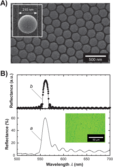 | ||
| Fig. 1 (A) Scanning electron microscopy (SEM) image observed from the top-view direction of a CC film of synthesized PS microparticles stabilized by a PDMS matrix. The white scale bar denotes 500 nm. The inset represents an SEM image of a discretely single PS microparticle synthesized by emulsion polymerization. (B) Theoretical reflection (upper: spectrum b) and experimental local-reflection (lower: spectrum a) spectra of a CC film of PS–PDMS. The theoretical reflection spectrum was calculated by the scalar wave approximation (SWA) technique.12 In this experiment, the measuring area of the local reflection spectrum was restricted to a diameter of ∼100 μm in the CC film. The inset shows a microscopic image of reflection color observed from the CC film of PS–PDMS. The white scale bar represents 50 μm. | ||
Using the synthesized PS microparticles, we fabricated CC films through a natural drying technique of the aqueous colloidal suspension with silicone oil.10 After complete self-assembly of a CC film, a solution of poly(dimethylsiloxane) (PDMS) precursor was infiltrated into the void space between PS microparticles. Finally, the PDMS precursor was substantially immobilized by thermal polymerization to give a homogeneous and stable CC film of PS–PDMS. The fabrication procedure is described in detail in the Experimental section.
In order to evaluate the optical characteristics at a microscopic level, we constructed an original optical system to obtain local reflection spectra of the CC film as well as to observe, in situ, their reflection microscopic images (Fig. S1, ESI†). The details are given in the Experimental section. As will be seen below, our system enables not only the measurements of both local reflection and local emission spectra from the same area, but also the in situ observation of reflection and emission optical images.
The as-prepared CC film showed a characteristic reflection band of the PBG in a wavelength range from 550 nm to 570 nm. At the same time, the reflectance reached ∼60% in the peak intensity (spectrum a, Fig. 1B). We observed Fabry–Perót interference fringes around the reflection band, implying the uniformity of the CC film thickness over a large area.11 The microscopic reflection color was observed to be clear green (inset, Fig. 1B). Moreover, scanning electron microscopy (SEM) observation allows us to visualize the ordered CC structures of PS microparticles on a microscopic scale. The SEM observations from the top view direction proved that this CC film adopts the close-packed structure of PS microparticles (Fig. 1A). Furthermore, when observed from the cross-sectional direction, we could not confirm the obvious surface roughness of the CC film of PS–PDMS (Fig. S2, ESI†). The as-prepared CC film showed a relatively flat surface and a film thickness of ∼14 μm in a large area with 1.0 × 103 μm2 or more. Moreover, we found that the outermost surface of the CC film is almost parallel with the substrate surface. From the SEM images, the lattice spacing was estimated to be 195 nm.
The theoretical reflection spectrum of this CC film can be calculated by the scalar wave approximation (SWA) technique6,12 in combination with empirical parameters such as lattice spacing, thickness of the CC film and refractive indices of PS and PDMS (spectrum b, Fig. 1B). As a result, the theoretical reflection spectrum was rather similar in appearance to the corresponding experimental spectrum. In particular, the theoretical reflection wavelength and bandwidth were in a reasonably good agreement with the experimental results.
2.2. Preparation of a photochromic light-emitting layer and its spectral properties
As the photochromic light-emitting material in the planar defect of the CC-L cavity (Scheme 1), we herein used four types of chemical compounds—1,2-bis[2-methylbenzo[b]thiophen-3-yl]-3,3,4,4,5,5-hexafluoro-1-cyclopentene (BDTH) as a photochromic diarylethene compound, a 1,3,5,7,8-pentamethyl-2,6-diethylpyrromethene-difluoroborate complex (PM) as a light-emitting compound, ethoxylated trimethylolpropane triacrylate (ETT) as a fluid host oligomer and bis(2,4,6-trimethylbenzoyl)phenylphosphine oxide (BPO) as a photopolymerization initiator. Details of preparation and fabrication procedures are given in the Experimental section.In this study, BDTH was adopted as the photochromic compound because it exhibits an excellent bistable characteristic by alternating irradiation with UV light at 313 nm and visible light at 530 nm, resulting in the photochromic reaction between an open-ring form (BDTH-O) and closed-ring form (BDTH-C) (Scheme 1).13Fig. 2A shows the changes in absorption spectra of a photochromic film of BDTH solely dissolved in ETT upon irradiation with 313 nm light (upper spectra) and the subsequent irradiation with 530 nm light (lower spectra). In its initial state, BDTH-O showed a highly optical transparency due to no intrinsic molar absorption coefficient above 400 nm. When BDTH-O was irradiated with 313 nm light, we observed continuously increasing intensities in a broad absorption band at ∼580 nm by the photocyclization from BDTH-O to BDTH-C, in accordance with the Woodward–Hoffmann rule (upper spectra, Fig. 2A). At this state, the BDTH-C film exhibited dark purple color. Subsequently, the colored BDTH-C could return to the initial colorless BDTH-O due to the photocycloreversion by irradiation with 530 nm light (lower spectra, Fig. 2A). We found that the absorption spectra are continuously changed in the presence of an isosbestic point at ∼293 nm during irradiation with both 313 nm and 530 nm light (insets of upper and lower spectra, Fig. 2A). This result provides clear evidence that there is no formation of aggregated BDTH in the ETT matrix.
 | ||
| Fig. 2 (A) Changes in absorption spectra of a photochromic film of BDTH solely dissolved in ETT upon irradiation with UV light at 313 nm (upper) and the subsequent irradiation with visible light at 530 nm (lower). The insets of the figures represent the spectral changes magnified around 293 nm. Note that the absorption spectra are continuously changed in the presence of an isosbestic point at ∼293 nm during the photoirradiation not only with 313 nm light, but also with 530 nm light. (B) Absorption (dashed spectrum) and fluorescence spectra (solid spectrum) of a light-emitting film of PM solely dissolved in ETT. The fluorescence spectrum was measured by excitation with 470 nm light from an Xe lamp. | ||
As the light-emitting compound, we used a pyrromethene complex of PM. This PM complex is known to have a high molar extinction coefficient and a high quantum fluorescence yield,14 thereby leading to the possibility to generate the laser feedback effect efficiently. When the PM complex was dispersed in the ETT matrix, we observed characteristic absorption and fluorescence bands at 520 nm and 542 nm, respectively (Fig. 2B). Compared with the absorption spectra of BDTH, the fluorescence spectral band of PM with the maximum wavelength of 542 nm overlaps well with the broad absorption band of BDTH-C with the maximum wavelength of ∼580 nm (Fig. 2A and B). Hence, we anticipate that when the PM complex is doped in photochromic BDTH, the fluorescence signals of PM might be quenched by absorption of BDTH-C.13 Taking into account these preliminary experiments, we can envisage that appropriate addition of BDTH with PM enables the reversible photoswitching in fluorescence intensity of PM by the photochromic reaction of BDTH.13
In order to unravel the fundamental properties of a mixture of BDTH and PM at the ground and excited states, we then measured the changes in absorption and fluorescence spectra by alternating irradiation with 313 nm and 530 nm light. In this study, we prepared a photochromic light-emitting BDTH–PM film by mixing 1.0 wt% BDTH and 0.25 wt% PM in a photocrosslinkable ETT matrix with BPO. The absorption spectral changes are shown in Fig. 3A. The as-prepared BDTH–PM film dominantly showed two broad bands centered at 268 nm and 520 nm by electronic absorption bands of BDTH-O and PM, respectively (spectrum a, Fig. 3A). After irradiation with 313 nm light, two new absorption bands at 377 nm and 580 nm emerged due to the photocyclization from BDTH-O to BDTH-C (spectrum b, Fig. 3A). After scrutinizing the results, we found that the absorption spectral changes proceed in the absence of any isosbestic point at around 293 nm during irradiation with 313 nm light (inset, Fig. 3A). On the other hand, as shown in Fig. 2A, when a photochromic film of BDTH solely dissolved in ETT was irradiated with 313 nm light, followed by 530 nm light, we could observe an isosbestic point at ∼293 nm during both absorption spectral changes. Comparison of the absorption spectral changes of BDTH films with and without PM indicates the strong intermolecular interactions between BDTH and PM at the ground state in the initial state of the BDTH–PM film. Thereafter, photoirradiation with 530 nm light led to a monotonous decrease in the absorption bands at 377 nm and 580 nm by the photocycloreversion of BDTH, eventually resulting in the absorption intensity reverting to a level close to that observed in the initial state (spectrum c, Fig. 3A). Interestingly, during irradiation with 530 nm light, we found an isosbestic point at ∼293 nm in the course of the absorption spectral changes of this BDTH–PM film owing to no interaction between BDTH and PM (Fig. S3, ESI†). Therefore, it is plausible that the strong intermolecular interactions between PM and BDTH in the initial state film disappears by the photocycloreversion of BDTH induced by irradiation with 530 nm light.
 | ||
| Fig. 3 (A) Absorption spectra of a BDTH–PM film in its initial state (spectrum a: red line), photostationary states of irradiation with UV light at 313 nm (spectrum b: dotted black line) and under visible light at 530 nm (spectrum c: blue line). The inset represents the changes in absorption spectra around 293 nm of the initial state BDTH–PM film (spectrum a) during irradiation with 313 nm light (spectrum b). Dashed thin lines shown in this inset are the intermediate absorption spectra up to the photostationary state of the irradiation with 313 nm light. Note that these absorption spectral changes proceed in the absence of any isosbestic point during the photoirradiation with 313 nm light (from spectrum a to spectrum b). The absorption spectral changes around 293 nm by the subsequent irradiation with 530 nm light (from spectrum b to spectrum c) are shown in Fig. S3 of the ESI.† (B) Fluorescence spectra of a BDTH–PM film in its initial state (spectrum a: red line), photostationary states of irradiation with 313 nm light (spectrum b: dotted black line) and 530 nm light (spectrum c: blue line). The fluorescence spectra were measured by excitation with 470 nm light from an Xe lamp. | ||
Fluorescence spectral measurement provides invaluable information on intermolecular interactions between aromatic chromophores at the electronically excited states, leading to the intrinsic emission species such as monomer, excimer and exciplex fluorescence. The changes in the fluorescence spectra are shown in Fig. 3B. The initial state BDTH–PM film showed a fluorescence spectrum with the maximum wavelength (λFL) of 548 nm, whereupon the absolute fluorescence quantum yield (ΦFL) was 0.25 (spectrum a, Fig. 3B). Note that a film of PM solely dissolved in ETT exhibits a monomer fluorescence band with a λFL of 542 nm, as shown in Fig. 2B. Such a bathochromic shift of 6 nm in λFL for BDTH–PM can be rationalized in terms of the formation of an exciplex of PM and BDTH. Photoirradiation with 313 nm light led to reduction in the fluorescence intensity of PM, eventually resulting in a remarkably low ΦFL value minimized at 0.01 for the photostationary state (spectrum b, Fig. 3B). This experimental fact allows strong fluorescence quenching by the intermolecular energy transfer from PM (as donor) to BDTH-C (as acceptor).13 When the irradiating light was switched from 313 nm to 530 nm, the fluorescence intensity reversibly increased with a concomitant increase in ΦFL value to 0.29 (spectrum c, Fig. 3B). Interestingly, the λFL after irradiation with 313 nm and 530 nm light shifted to a shorter wavelength of 542 nm, as compared with that of the initial state. This result implies that the exciplex of PM and BDTH in the initial state film is decoupled by the photochromic reaction of BDTH, leading to the formation of monomeric PM. This interpretation is fairly consistent with the following experimental result: the ΦFL value of the BDTH–PM film after irradiation with 313 nm and 530 nm light (ΦFL = 0.29) is higher than that of the initial state (ΦFL = 0.25) because the monomer fluorescence is typically a high ΦFL value.
We then pursued the repetitive changes in ΦFL and absorbance at 580 nm of the BDTH–PM film as a function of the total time of alternating irradiation with 313 nm and 530 nm light. The results are shown in Fig. 4. The profiles showed the synchronous changes between ΦFL and absorbance at 580 nm by alternate photoirradiation. The absorbance at 580 nm increased as the ΦFL value decreased for irradiation with 313 nm light, and vice versa with 530 nm light. The changes were reversible. In this way, we accomplished the photoswitching of fluorescence intensity of PM by alternating irradiation with 313 nm and 530 nm light through the photochromic reaction of BDTH.
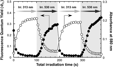 | ||
| Fig. 4 Continuous changes in absolute fluorescence quantum yields (ΦFL) (closed circles) and absorbances at 580 nm (open circles) of a BDTH–PM film as a function of total irradiation time of alternating 313 nm (white region) and 530 nm (gray region) light. The increase of absorbance at 580 nm by irradiation with 313 nm light is attributed to photocyclization from BDTH-O to BDTH-C, thereby resulting in the decrease of ΦFL from PM, and vice versa with 530 nm light. | ||
2.3. Fabrication of the CC-L cavity and its SEM observation
In order to achieve the efficient laser feedback effect by our designed CC-L cavity (Scheme 1), we should consider the following important requirement: the reflection band of CC films should overlap with the optical gain spectrum of BDTH–PM in the planar defect.6 Commonly, the optical gain spectrum has an analogous spectral shape to the fluorescence spectrum. Comparing the reflection and fluorescence spectra (Fig. 1B and 3B) reconfirms that the combination of a PS–PDMS CC film with a BDTH–PM planar defect would be suitable for the efficient generation of the laser feedback effect.We fabricated a CC-L cavity comprising a photochromic light-emitting planar defect of BDTH–PM between a pair of CC films of PS–PDMS, according to a procedure described in the Experimental section. The microscopic structure of the CC-L cavity was confirmed by the cross-sectional SEM observation, as shown in Fig. 5. It was found that the photochromic light-emitting planar defect of BDTH–PM with a thickness of ∼2.7 μm is homogeneously localized between a pair of CC films of PS–PDMS.
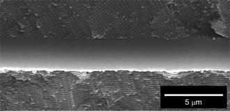 | ||
| Fig. 5 A magnified cross-sectional SEM image of a photochromic light-emitting planar defect of BDTH–PM embedded between a pair of CC films of PS–PDMS in the CC-L cavity. The white scale bar represents 5 μm. | ||
2.4. Lasing properties of the CC-L cavity
The laser emission properties from the microscopic area of the CC-L cavity were evaluated by optical excitation with 470 nm light from a Nd:yttrium aluminum garnet (Nd:YAG) laser beam equipped with an optical parametric oscillator (OPO), which was directly adapted into a motorized illuminator for an optical microscope (Fig. S1, ESI†). The details are described in the Experimental section. Fig. 6A shows the changes in emission spectra of the CC-L cavity before and after optically excited lasing action. By optical excitation with a pulse energy of 29 nJ per pulse, we observed the following anomalous variation in the emission spectrum of the BDTH–PM (spectrum a, Fig. 6A): a broad emission spectrum was remarkably forbidden in the wavelength range of a reflection band of the CC film (Fig. 1B). This result implies that the reflection band of CC films works as the PBG, leading to strong confinement of the emitting photons from the planar defect in the orthogonal direction of this CC-L cavity. When the excitation energy was increased to 38 nJ per pulse, we observed a single and narrow laser emission peak at ∼560 nm (spectrum b, Fig. 6A). In addition, the microscopic emission images were drastically changed before and after the lasing action (Fig. S4, ESI†). We could observe stably the single laser emission peak from the CC-L cavity during the experiment time over several hours. This is because the threshold excitation peak power of our CC-L cavity for laser action is quite low, as compared to the previous reports on lasing action from the other CC cavities (vide infra). After the lasing experiment, we could not observe structural deterioration in the CC films, such as laser ablation, due to no intrinsic absorption bands of PS and PDMS at an optical exaction wavelength of 470 nm as well as a low threshold excitation peak power for lasing action. Also, we could avoid obvious photobleaching of BDTH–PM because the mixture was degassed by evacuation in vacuo to remove oxygen, which typically generates the photobleaching of organic dyes, before fabrication of the CC-L cavity, as described in the Experimental section. | ||
| Fig. 6 (A) Microscopic emission spectra from a CC-L cavity with a photochromic light-emitting BDTH–PM planar defect by optical excitation with 470 nm light with the pulse energies of 29 nJ per pulse (spectrum a) and 38 nJ per pulse (spectrum b). Spectrum a is magnified 8 times in the emission intensity to confirm the spectrum shape. A gray arrow represents the theoretical wavelength of the defect mode in the CC-L cavity calculated on the basis of the SWA results of the CC film. The inset shows a high resolution spectrum of the laser emission magnified around 560 nm. (B) Microscopic reflection spectrum of the CC-L cavity with a BDTH–PM planar defect. (C) Changes in the emission intensity at ∼560 nm of the CC-L cavity as a function of the pulse energy of optical excitation with 470 nm light. This CC-L cavity was irradiated beforehand with 313 nm light (green squares) and 530 nm light (red circles) in the photostationary state. | ||
It is plausible that the single laser emission peak within the reflection band of the CC film is caused by the defect mode localized in the PBG of the CC film.6 However, there was no obvious appearance of the defect mode peak in the reflection spectrum of the CC-L cavity, as shown in Fig. 6B, because the defect mode peak disappears due to the absorption band of the photochromic light-emitting planar defect of BDTH–PM between the CC films.6,15 In fact, we observed an absorption band of BDTH–PM expanding to 560 nm (Fig. 3A), which overlaps with the reflection band of the CC film of PS–PDMS with the maximum wavelength of 560 nm (Fig. 1B). Such observation is consistent even when light-emitting organic planar defects are embedded between a pair of 1D-PC films, such as dielectric multilayered mirrors and cholesteric liquid crystals.16 As evident from the precedents, it is not easy to detect the defect mode peaks within the PBG by both transmission and reflection spectral measurements when the PBG wavelength range of PCs overlaps with the absorption band of planar defects embedded between the PC structures.
In order to understand the laser mechanism of this CC-L cavity from a theoretical viewpoint, we calculated the theoretical wavelength of the defect mode peak which appeared in the PBG wavelength range. By considering the oscillation conditions, the theoretical defect mode wavelength could be calculated from the SWA results of the CC film with the thickness and refractive index of the BDTH–PM planar defect. The light wave in the PBG can be expressed as the following equation:12
| EPBG(x) = CPBGe−qxcos(Gx/2 + δ) | (1) |
| Ed(x) = Cdcos(kdx) or C′dsin(kdx) | (2) |
It should be stressed that such a single lasing peak can be rationalized by considering the fact that the free spectral range (FSR)15 of this CC-L cavity is wider than the PBG wavelength range of the CC film.6 Indeed, the FSR of this CC-L cavity was estimated to be 36.1 THz whereas the PBG wavelength range of the CC film was 19.1 THz.17
At this lasing stage, we measured a high resolution emission spectrum (inset, Fig. 6A). We found that the spectral linewidth (Δλ) is as narrow as 0.16 nm. In order to quantitatively compare this laser emission with those in the previous reports, we estimated the quality factor (Q) from the high resolution laser emission spectrum. According to the previous reports,18 the Q value can be generally expressed as the following equation:
| Q = λ/Δλ | (3) |
2.5. Photoswitchable lasing by alternating irradiation with 313 nm and 530 nm light
Taking advantage of the photoswitchable fluorescence intensity of BDTH–PM (Fig. 3B and 4), we attempted to control the lasing action from the CC-L cavity by alternating photoirradiation with 313 nm and 530 nm light. In order to determine the threshold excitation energy (or peak power) for the laser feedback effect, we investigated the changes in emission intensity at a lasing wavelength of ∼560 nm while increasing the pulse energy of optical excitation. The results are shown in Fig. 6C.Beforehand, when the CC-L cavity had been irradiated with 530 nm light, the single laser emission peak was generated by optical excitation with 470 nm light at a low threshold energy (red circles, Fig. 6C). When the excitation energy exceeded 36 nJ per pulse, the emission significantly intensified with a concurrent narrowing of the spectral linewidth to 0.16 nm. In this study, the pulse duration and the focused diameter of the excitation beam were set at ∼6 ns and ∼36 μm, respectively. Therefore, the lasing threshold peak power was estimated to be ∼590 kW cm−2. More importantly, to our knowledge, this threshold peak power is a quite low value compared to the precedents of lasing action from the other cavities fabricated with CCs.19 The present CC-L cavity is not optimal; however tailoring the materials and cavity structures enables further reduction in the threshold excitation power. Thereby, we would realize the continuous wave (CW)-excited laser devices with versatile practical applications.20
Contrary to this observation for the CC-L cavity irradiated with 530 nm light, it was found that no lasing action is generated at all for the CC-L cavity irradiated with 313 nm light in advance (green squares, Fig. 6C). With the above fluorescence results of BDTH–PM in mind (spectrum b, Fig. 3B), it is most likely that the ΦFL value after irradiation with 313 nm light (ΦFL = 0.01) is inadequate for generation of the laser feedback effect. When the CC-L cavity was optically excited with pulse energies above 36 nJ per pulse, we observed high contrasts in the emission intensities between the CC-L cavity irradiated beforehand with 530 nm light and that with 313 nm light: the emission intensities of the CC-L cavity irradiated with 530 nm light were over 3 orders of magnitude higher than those with 313 nm light. In this way, we succeeded in the reversible photoswitching of optically excited laser action by alternating irradiation with 313 nm and 530 nm light.
2.6. Micropattened lasing from a CC-L cavity inscribed by photoirradiation
Finally, as a technical extension of our findings, we successfully demonstrated the micropatterned lasing from the CC-L cavity. Fig. 7 highlights the most essential performance of our CC-L cavity. In this experiment, a CC-L cavity was irradiated with 313 nm light through a photomask (upper images, Fig. 7) to inscribe a micropattern in the BDTH–PM planar defect. After removing the photomask, the microscopic images for laser emission were acquired by optical excitation with 470 nm light through our original optical microscopic system (Fig. S1, ESI†). To obtain clear lasing images, the emission intensity was attenuated by neutral density (ND) filters. Most interestingly, we could observe the high contrast micropatterned lasing images with various shapes of the photomasks (lower images, Fig. 7). The masked region emitted a bright green color as laser emission, whereas the unmasked regions showed dark images.21 Importantly, the micropatterned laser images from the CC-L cavity could be rewritten by photoirradiation with 530 nm for erasing the previous images, and the subsequent irradiation with 313 nm light through various photomasks for writing the new images. At present, we achieved a micropatterned lasing image with a high resolution of only a few micrometers (rightmost lower image, Fig. 7). This resolution of the micropatterned images of a single laser emission peak with a narrow band observed from the CC-L cavity is in a very high level, as compared with that of the patterned images of the spontaneous emission with a broad band, i.e. fluorescence, from a photochromic light-emitting polymer film on a CC film.8 Thus, we succeeded in the on-demand and reversible control of micropatterned lasing images from our CC-L cavity by the photoirradiation through photomasks. Taking overall results into account, such reversibly dynamic photoswitching of micropatterned laser emission with a single and narrow peak provides new breakthroughs to fabricate the small sized and high density all-optical photoswitching devices.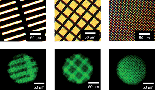 | ||
| Fig. 7 Micropatterned images of laser emission from the CC-L cavity, which was inscribed beforehand by irradiation with 313 nm light through various photomasks. The upper images show microscopic transmission images of various photomasks used in this study and the lower images are microscopic images of micropatterned laser emission observed from the CC-L cavity. Optical excitation with 470 nm light was carried out through an objective lens with 5× to obtain a circular spot on the CC-L cavity with a diameter of ∼145 μm. The emission intensity was attenuated by ND filters to obtain clear microscopic images of laser emission. The white scale bars represent 50 μm. | ||
3. Conclusions
In conclusion, we have presented the first example of reversible photoswitching of micropatterned lasing from a CC-L cavity by alternating irradiation with 313 nm and 530 nm light. This CC-L cavity structure consists of a photochromic light-emitting planar defect of BDTH and PM embedded between a pair of polymer CC films (Scheme 1). Optical excitation of the CC-L cavity with 470 nm light generates a single and very narrow lasing peak at ∼560 nm within the reflection band of CC films due to the defect mode localized in the PBG. The optically excited lasing action can be dynamically switched by alternating irradiation with 313 nm and 530 nm light as a result of the intermolecular energy transfer induced by the photochromic reaction of BDTH. Moreover, we successfully demonstrated the high contrast micropatterned lasing action with a high resolution of only a few micrometers. Such various micropatterned images of laser emission can be erased and rewritten by alternating photoirradiation with 313 nm and 530 nm through photomasks.From a practical viewpoint, the dynamic photoswitching of micropatterned lasing with a single and narrow peak is greatly advantageous for the fabrication of high density photonic and display devices.22 Such photoswitching of micropatterned lasing is not limited to the CC system. We envisage that unique laser performances can be generated by applying the photochromic light-emitting materials in various PC systems such as 1D-, 2D- and 3D-PCs. Thus, our successful findings provide promising breakthroughs not only to realize the on-demand photocontrol of the laser feedback effect by the photochromic compounds, but also to fabricate the small-sized and high density photoswitchable devices for all-optical integrated circuits. Currently, technological development towards high performance lasers is in progress through the combination of stable light-emitting inorganic nanomaterials such as quantum dots or a variety of cavity structures.23
4. Experimental
4.1. General instruments
Absorption spectra were taken on a photodiode array spectrometer (8453, Agilent). Photoirradiation with 313 nm light was carried out by a 150 W Hg–Xe lamp (UV Supercure-203S, San-ei Electric) through a solution filter of K2CrO4 in 0.1 N NaOH and a band-pass filter (UV-D35, Toshiba) to isolate the 313 nm light. For irradiation with 530 nm light, we used a compact Xe lamp (MAX-302-vis, Asahi Spectra) combined with a band-pass filter of 530 ± 10 nm. The light intensities of 313 nm and 530 nm light were tuned at ∼5 mW cm−2 and ∼10 mW cm−2, respectively. Fluorescence spectra were recorded on a spectrofluorophotometer (RF-5300PC, Shimadzu). Fluorescence quantum yields were evaluated by a measurement system of absolute photoluminescnce quantum yield (C9920-02G, Hamamatsu Photonics) equipped with a photonic multichannel analyzer (C10027-01, Hamamatsu Photonics). For both fluorescence spectral and fluorescence quantum yield measurements, the excitation wavelength was set at 470 nm. Scanning electron microscopy (SEM) images were obtained by a field emission scanning electron microscope (JSM-6500F, JEOL). Microparticle size distribution was determined by a dynamic light scattering measurement system (Nanotrac Wave-UT151, Nikkiso). Refractive indices of materials were obtained by an Abbe refractometer (NAR-2T-HI, Atago).4.2. Synthesis of PS microparticles
We synthesized the monodispersed PS microparticles with a diameter of ∼210 nm by emulsion polymerization of a styrene monomer in the presence of sodium dodecyl sulfate (SDS) as a surfactant. First, 0.6 g of SDS and 0.5 g of sodium hydrogen carbonate (SHC) were dissolved in 600 ml of deionized water in a four-neck flask. Subsequently, 60 g of styrene monomer was dispersed in the aqueous solution of SDS and SHC. The aqueous solution was stirred at ∼250 rpm and refluxed at 80 °C under nitrogen atmosphere for 5 h to completely form the SDS micelle aggregations with the styrene monomer in water. After that, the stirring solution was added by dropping a solution of 0.5 g of potassium persulfate (KPS), as a thermal polymerization initiator, in 50 ml of deionized water for 30 min. The solution was continuously stirred and refluxed at 80 °C for 24 h. After complete polymerization, the resultant aqueous suspension of PS microparticles was filtered through a filter paper and membrane filters with pore sizes of 5.0 μm and 1.2 μm. The filtered suspension was rigorously centrifuged at 1.5 × 10⁴ rpm for 100 min in order to remove the low molecular weight components such as SDS, SHC and KPS in the supernatant liquid. Finally, the aqueous suspension of PS microparticles was purified by deionization with ion-exchange resin three times.4.3. Fabrication of CC films
Using the synthesized PS microparticles, we fabricated CC films on synthetic quartz glass substrates by a natural drying technique of the aqueous suspension of PS microparticles covered with silicone oil.10 In this study, we used the synthetic quartz glass substrate because of its high transparency above 200 nm. Before fabricating the CC film of PS microparticles, synthetic quartz glass substrates were treated with oxygen plasma to obtain a hydrophilic surface. The as-prepared CC film of PS microparticles was not stable due to the existence of fluid silicone oil in the void space between the microparticles. However, in order to stabilize the CC film, the void space was occupied by a PDMS precursor. After thermal polymerization of the PDMS precursor at room temperature for 12 h and 60 °C for 3 h, we obtained a flat and stable CC film of PS microparticles embedded in the PDMS matrix.4.4. Fabrication of the CC-L cavity
We designed and fabricated a photochromic light-emitting colloidal crystal-laser (CC-L) cavity for reversibly dynamic photoswitching of micropatterned laser action (Scheme 1). Our CC-L cavity consists of a photochromic light-emitting planar defect of BDTH–PM between a pair of colloidal crystal (CC) films of PS–PDMS.In order to fabricate the CC-L cavity, we clipped ∼1 cm2 high quality CC parts from the large as-prepared film. The photochromic light-emitting material used in the planar defect was prepared by mixing BDTH as a photochromic diarylethene compound, PM as a light-emitting compound, ETT as a fluid host oligomer and BPO as a photopolymerization initiator in the weight ratio of 1.0![[thin space (1/6-em)]](https://www.rsc.org/images/entities/char_2009.gif) :0.25:0.5:98, respectively. Before fabricating the CC-L cavity, the mixture of BDTH, PM, ETT and BPO was degassed by evacuation in vacuo to remove oxygen. After that, the fluid mixture was smoothly injected between a pair of CC films through capillary force. The thickness between the CC films was adjusted using silica particles with a diameter of ∼2.7 μm. Finally, the ETT oligomer was photopolymerized by irradiation with 405 nm light in order to substantially immobilize the photochromic light-emitting planar defect of BDTH–PM between the CC films of PS–PMDS.
:0.25:0.5:98, respectively. Before fabricating the CC-L cavity, the mixture of BDTH, PM, ETT and BPO was degassed by evacuation in vacuo to remove oxygen. After that, the fluid mixture was smoothly injected between a pair of CC films through capillary force. The thickness between the CC films was adjusted using silica particles with a diameter of ∼2.7 μm. Finally, the ETT oligomer was photopolymerized by irradiation with 405 nm light in order to substantially immobilize the photochromic light-emitting planar defect of BDTH–PM between the CC films of PS–PMDS.
4.5. Microscopic optical measurements
In order to investigate the microscopic optical characteristics, we constructed an original optical microscopic system to enable not only measurements of local reflection and emission spectra of the CC-L cavity, but also in situ observations of their microscopic optical images (Fig. S1, ESI†). The local reflection spectra were collected through a motorized illuminator for a microscope (BX-RLA2, Olympus) with a 100 W halogen lamp. Concurrently, the local emission spectra of the CC-L cavity were measured by optical excitation with 470 nm light from an OPO excited by the third harmonic light at 355 nm from a Q-switched Nd:YAG laser beam (Surelite I-10 and OPO Plus, Continuum). The pulse width was ∼6 ns and the repetition frequency was 10 Hz. The excitation pulse energy was controlled by a λ/2 plate, a Gran-Laser prism and ND filters, and was monitored by using an energy analyzer equipped with a pyroelectric sensor (PE-9, Ophir). The excitation beam propagated along the surface normal of the CC-L cavity, and it was focused using a microscope objective lens with 20× or 5× to acquire a circular spot with ∼36 μm or ∼145 μm in diameter on the CC-L cavity, respectively. The collinearly transmitted emission spectra from the CC-L cavity were recorded on a highly sensitive charge-coupled device spectrometer (SR-303i and iDus DU420A, Andor Technology). Concurrently, the microscopic reflection and emission color images were taken by a complementary metal oxide semiconductor camera (Moticam2000, Shimadzu).Acknowledgements
This work was supported, in part, by the Grant-in-Aid for Young Scientist (A) from Ministry of Education, Science, Sports and Culture and the Yazaki Memorial Foundation for Science and Technology of Japan. S.F. is deeply indebted to Ms Kaori Terui and Dr Hideki T. Miyazaki of the NIMS for experimental assistance and technical advices, respectively. Furthermore, S.F. thanks Mr Kazuya Kanda of the Nikkiso Co., Ltd for dynamic light scattering measurements.Notes and references
- (a) S. John, Phys. Rev. Lett., 1987, 58, 2486 CrossRef CAS PubMed; (b) E. Yablonovitch, Phys. Rev. Lett., 1987, 58, 2059 CrossRef CAS PubMed.
- C. López, Adv. Mater., 2003, 15, 1679 CrossRef.
- (a) A. Blannco, E. Chomski, S. Grabtchak, M. Ibisate, S. John, S. W. Leonard, C. López, F. Meseguer, H. Mìguez, J. P. Mondia, G. A. Ozin, O. Toader and H. M. van Driel, Nature, 2000, 405, 437 CrossRef PubMed; (b) S. Noda, K. Tomoda, N. Yamamoto and A. Chutinan, Science, 2000, 289, 604 CrossRef CAS PubMed.
- For reviews see e.g. (a) Y. Xia, B. Gates, Y. Yin and Y. Lu, Adv. Mater., 2000, 12, 693 CrossRef CAS; (b) V. L. Colvin, MRS Bull., 2001, 26, 637 CrossRef CAS; (c) G. A. Ozin and S. M. Yang, Adv. Funct. Mater., 2001, 11, 95 CrossRef CAS; (d) Q. Yan, L. Wang and X. S. Zhao, Adv. Funct. Mater., 2007, 17, 3695 CrossRef CAS; (e) O. Sato, S. Kubo and Z.-Z. Gu, Acc. Chem. Res., 2009, 42, 1 CrossRef CAS PubMed; (f) M. Harun-Ur-Rashid, T. Seki and Y. Takeoka, Chem. Rec., 2009, 9, 87 CrossRef CAS PubMed; (g) S. Furumi, H. Fudouzi and T. Sawada, Laser Photonics Rev., 2010, 4, 205 CrossRef CAS; (h) C. I. Aguirre, E. Reguera and A. Stein, Adv. Funct. Mater., 2010, 20, 2565 CrossRef CAS; (i) K. A. Arpin, A. Mihi, H. T. Johnson, A. J. Baca, J. A. Rogers, J. A. Lewis and P. V. Braun, Adv. Mater., 2010, 22, 1084 CrossRef CAS PubMed; (j) J. F. Galisteo-López, M. Ibisate, R. Sapienza, L. S. Froufe-Pérez, Á. Blanco and C. López, Adv. Mater., 2011, 23, 30 CrossRef PubMed; (k) S.-H. Kim, S. Y. Lee, S.-M. Yang and G.-R. Yi, NPG Asia Mater., 2011, 3, 25 CrossRef CAS; (l) J. Ge and Y. Yin, Angew. Chem., Int. Ed., 2011, 50, 1492 CrossRef CAS PubMed; (m) S. Furumi, Nanoscale, 2012, 4, 5564 RSC.
- (a) S. A. Asher, J. Holtz, L. Liu and Z. Wu, J. Am. Chem. Soc., 1994, 116, 4997 CrossRef CAS; (b) J. M. Wessman, H. B. Sunkara, A. S. Tse and S. A. Asher, Science, 1996, 274, 959 CrossRef; (c) J. H. Holtz and S. A. Asher, Nature, 1997, 389, 829 CrossRef CAS PubMed; (d) L. Liu, P. Li and S. A. Asher, Nature, 1999, 397, 141 CrossRef CAS PubMed; (e) R. C. Schroden, M. Al-Daous, C. F. Blanford and A. Stein, Chem. Mater., 2002, 14, 3305 CrossRef CAS; (f) S. Kubo, Z.-Z. Gu, K. Takahashi, Y. Ohko, O. Sato and A. Fujishima, J. Am. Chem. Soc., 2002, 124, 10950 CrossRef CAS PubMed; (g) H. Saito, Y. Takeoka and M. Watanabe, Chem. Commun., 2003, 2126 RSC; (h) Y.-J. Lee and P. V. Braun, Adv. Mater., 2003, 15, 563 CrossRef CAS; (i) D. Nakayama, Y. Takeoka, M. Watanabe and K. Kataoka, Angew. Chem., Int. Ed., 2003, 42, 4197 CrossRef CAS PubMed; (j) M. Kamenjicki, I. K. Lednev, A. Mikhonin, R. Kesavamoorthy and S. A. Asher, Adv. Funct. Mater., 2003, 13, 774 CrossRef CAS; (k) R. A. Barry and P. Wiltzius, Langmuir, 2006, 22, 1369 CrossRef CAS PubMed; (l) A. C. Arsenault, T. J. Clark, G. V. Freymann, L. Cademartiri, R. Sapienza, J. Bertolotti, E. Verkris, S. Wong, V. Kitaev, I. Manners, R. Z. Wang, S. John, D. Wiersma and G. A. Ozin, Nat. Mater., 2006, 5, 179 CrossRef CAS; (m) A. C. Arsenault, D. P. Puzzo, I. Manners and G. A. Ozin, Nat. Photonics, 2007, 1, 468 CrossRef CAS; (n) J. Ge, Y. Hu and Y. Yin, Angew. Chem., Int. Ed., 2007, 46, 7428 CrossRef CAS PubMed.
- S. Furumi, H. Fudouzi, H. T. Miyazaki and Y. Sakka, Adv. Mater., 2007, 19, 2067 CrossRef CAS.
- H. Furukawa, M. Misu, K. Ando and H. Kawaguchi, Macromol. Rapid Commun., 2008, 29, 547 CrossRef CAS.
- H. Li, J. Wang, H. Lin, L. Xu, W. Xu, R. Wang, Y. Song and D. Zhu, Adv. Mater., 2010, 22, 1237 CrossRef CAS PubMed.
- S. Furumi, unpublished results.
- H. Fudouzi, J. Colloid Interface Sci., 2004, 275, 277 CrossRef CAS PubMed.
- S. Wong, V. Kitaev and G. A. Ozin, J. Am. Chem. Soc., 2003, 125, 15589 CrossRef CAS PubMed.
- (a) K. W.-K. Shung and Y. C. Tsai, Phys. Rev. B: Condens. Matter Mater. Phys., 1993, 48, 11265 CrossRef; (b) D. M. Mittleman, J. F. Bertone, P. Jiang, K. S. Hwang and V. L. Colvin, J. Chem. Phys., 1999, 111, 345 CrossRef CAS.
- (a) M. Irie, Chem. Rev., 2000, 100, 1685 CrossRef CAS PubMed; (b) K. Matsuda and M. Irie, J. Photochem. Photobiol., C, 2004, 5, 169 CrossRef CAS; (c) J. F. M. Raymo and M. Tomasulo, Chem. Soc. Rev., 2005, 34, 327 RSC; (d) H. Tian and S. Wang, Chem. Commun., 2007, 781 RSC; (e) T. Fukaminato, J. Photochem. Photobiol., C, 2011, 12, 177 CrossRef CAS.
- (a) S. C. Guggenheimer, J. H. Boyer, K. Thangaraj, M. Shah, M.-L. Soong and T. G. Pavlopoulos, Appl. Opt., 1993, 32, 3942 CrossRef CAS PubMed; (b) T. A. Golovkova, D. V. Kozlov and D. C. Neckers, J. Org. Chem., 2005, 70, 5545 CrossRef CAS PubMed; (c) W. Qin, M. Baruah, M. van der Auweraer, F. C. de Schryver and N. Boens, J. Phys. Chem. A, 2005, 109, 7371 CrossRef CAS PubMed.
- (a) A. Yariv and P. Yeh, in Photonics: Optical Electronics in Modern Communications, Oxford University Press, USA, 6th edn, 2006, Ch. 4 Search PubMed; (b) P. Mächtle, C. Müller and C. A. Helm, J. Phys. II, 1994, 4, 481 CrossRef.
- (a) R. Ozaki, T. Matsui, M. Ozaki and K. Yoshino, Appl. Phys. Lett., 2003, 82, 3593 CrossRef CAS; (b) R. Ozaki, Y. Matsuhisa, M. Ozaki and K. Yoshino, Appl. Phys. Lett., 2004, 84, 1844 CrossRef CAS; (c) M. H. Song, K.-C. Shin, B. Park, Y. Takanishi, K. Ishikawa, J. Watanabe, S. Nishimura, T. Toyooka, Z. Zhu, T. M. Swager and H. Takezoe, Sci. Technol. Adv. Mater., 2004, 5, 437 CrossRef CAS; (d) Y. Matsuhisa, R. Ozaki, M. Ozaki and K. Yoshino, Jpn. J. Appl. Phys., 2005, 44, L629 CrossRef CAS; (e) J. Yoon, W. Lee, J.-M. Caruge, M. Bawendi, E. L. Thomas, S. Kooi and P. N. Prasad, Appl. Phys. Lett., 2006, 88, 091102 CrossRef; (f) S. M. Jeong, N. Y. Ha, Y. Takanishi, K. Ishikawa, H. Takezoe, S. Nishimura and G. Suzaki, Appl. Phys. Lett., 2007, 90, 261108 CrossRef.
- The free spectral range (FSR) (ΔνFSR) means the frequency separation between the resonance wavelength (νm) and the neighboring one (νm+1). Here, m is any integer. ΔνFSR can be expressed as ΔνFSR = νm+1 − νm = c/2nd. In our CC-L cavity, d = 2.7 μm and n = 1.54. By using c = 3.0 × 10⁸ m s−1, the FSR of our laser cavity is calculated to be ΔνFSR = 36.1 THz. On the other hand, the photonic band gap (PBG) of our CC film determines the range of resonance frequency in the CC-L cavity. This is because the PBG range (ΔνPBG) of this CC film is narrower than the emission band of the PM dye used in the planar defect of this CC-L cavity. As seen in Fig. 1B, the PBG of this CC film appears from 550 nm (λ1) to 570 nm (λ2). From these values, ΔνPBG is estimated as ΔνPBG = c/λ1 − c/λ2 = 19.1 THz. Accordingly, the ΔνFSR value of this CC-L cavity is wider than ΔνPBG of this CC film. This means that the separation of Fabry–Perót modes in this CC-L cavity is sufficiently large. Therefore, our CC-L cavity supports a single resonance peak even though the planar defect embedded between a pair of CC films seems to be relatively thick of 2.7 μm.
- (a) J. D. Joannopoulos, P. R. Villeneuve and S. Fan, Nature, 1997, 386, 143 CrossRef CAS; (b) J. S. Foresi, P. R. Villeneuve, J. Ferrera, E. R. Thoen, G. Steinmeyer, S. Fan, J. D. Joannopoulos, L. C. Kimerling, H. I. Smith and E. P. Ippen, Nature, 1997, 390, 143 CrossRef CAS; (c) T. Someya, R. Werner, A. Forchel, M. Catalano, R. Cingolani and Y. Arakawa, Science, 1999, 285, 1905 CrossRef CAS PubMed; (d) M. Loncar, T. Yoshie, A. Scherer, P. Gogna and Y. Qui, Appl. Phys. Lett., 2002, 81, 2680 CrossRef CAS; (e) A. Tandaechanurat, S. Ishida, D. Guimard, M. Nomura, S. Iwamoto and Y. Arakawa, Nat. Photonics, 2011, 5, 91 CrossRef CAS.
- (a) K. Yoshino, S. Tatsuhara, Y. Kawaguchi, M. Ozaki, A. A. Zakhidov and Z. V. Vardeny, Jpn. J. Appl. Phys., 1998, 37, L1187 CAS; (b) M. N. Shkunov, Z. V. Vardeny, M. C. DeLong, R. C. Polson, A. A. Zakhidov and R. H. Baughman, Adv. Funct. Mater., 2002, 12, 21 CrossRef CAS; (c) J. R. Lawrence, Y. Ying, P. Jiang and S. H. Foulger, Adv. Mater., 2006, 18, 300 CrossRef CAS; (d) F. Jin, C.-F. Li, X.-Z. Dong, W.-Q. Chen and X.-M. Duan, Appl. Phys. Lett., 2006, 89, 241101 CrossRef; (e) H. Yamada, T. Nakamura, Y. Yamada and K. Yano, Adv. Mater., 2009, 21, 4134 CrossRef CAS; (f) S.-H. Kim, S.-H. Kim, W. C. Jeong and S.-M. Yang, Chem. Mater., 2009, 21, 4993 CrossRef CAS; (g) S. Furumi, T. Kanai and T. Sawada, Adv. Mater., 2011, 23, 3815 CAS.
- M. H. Song, B. Park, K.-C. Shin, T. Ohta, Y. Tsunoda, H. Hoshi, Y. Takanishi, K. Ishikawa, J. Watanabe, S. Nishimura, T. Toyooka, Z. Zhu, T. M. Swager and H. Takezoe, Adv. Mater., 2004, 16, 779 CrossRef CAS.
- Some darker regions in micropatterned laser images probably occurred by interference of 313 nm light for writing images through a photomask. Because the propagation of 313 nm light from an Xe lamp is not collimated.
- E. Miyai, K. Sakai, T. Okano, W. Kunishi, D. Ohnishi and S. Noda, Nature, 2006, 441, 946 CrossRef CAS PubMed.
- (a) S. Furumi, S. Yokoyama, A. Otomo and S. Mashiko, Appl. Phys. Lett., 2003, 82, 16 CrossRef CAS; (b) S. Furumi, S. Yokoyama, A. Otomo and S. Mashiko, Appl. Phys. Lett., 2004, 84, 2491 CrossRef CAS; (c) S. Furumi and Y. Sakka, Adv. Mater., 2006, 18, 775 CrossRef CAS; (d) S. Furumi, S. Yokoyama, A. Otomo and S. Mashiko, Thin Solid Films, 2006, 499, 322 CrossRef CAS; (e) S. Furumi and N. Tamaoki, Adv. Mater., 2010, 22, 886 CrossRef CAS PubMed; (f) S. Furumi, Chem. Rec., 2010, 10, 394 CAS.
Footnote |
| † Electronic supplementary information (ESI) available: Microscopic optical measurement setup, a cross-sectional SEM image of a single CC film, changes in absorption spectra of a photochromic light-emitting film, and microscopic emission images before and after optically excited laser action. |
| This journal is © The Royal Society of Chemistry 2012 |