Photo-induced amplification of readout contrast in nanoscale data storage†
Changqing
Ye
ab,
Mingzhu
Li
*a,
Jia
Luo
a,
Linfeng
Chen
ab,
Zhengming
Tang
c,
Jian
Pei
c,
Lei
Jiang
a,
Yanlin
Song
*a and
Daoben
Zhu
a
aBeijing National Laboratory for Molecular Sciences (BNLMS), Key Laboratory of Organic Solids, Laboratory of New Materials, Institute of Chemistry, Chinese Academy of Sciences, Beijing, 100190, P. R. China. E-mail: ylsong@iccas.ac.cn; mingzhu@iccas.ac.cn; Fax: (+86) 10-6252 9284
bGraduate University of Chinese Academy of Science, Beijing, 100049, P. R. China
cCollege of Chemistry and Molecular Engineering, Peking University, Beijing, 100871, China
First published on 19th January 2012
Abstract
A strategy to enhance the readout contrast of nanoscale data storage was achieved using light irradiation through the photo-induced amplification effect. This effect has shown wavelength-selective and light power-dependent characteristics. These results provided a new approach to enhancing the readout contrast of the STM recording image.
Introduction
The exponential growth in the globalization of information calls for the ever-increasing demands of the continuous miniaturization and the expansive storage capacity of memory devices.1 Among various recording strategies,2–7scanning probe microscopy including atomic force microscopy8,9 and scanning tunneling microscopy (STM)10–13 can achieve data recording at the nanometre or molecular scale, which is a powerful approach to conducting high-density data storage. STM is sensitive to local electronic properties and investigates molecules adsorbed on the solid substrates.14,15 As storage medium, rapid, reliable conductance switching with high ON/OFF ratio is essential for a memory device.16–18 At the current stage, most existing studies in the development of STM-based high-density storage make intense effort in the design and synthesis of novel functional materials with superior electrical bistable properties.19–21 Organic electric-responsive materials based on different bistable mechanisms have been developed, including intermolecular charge transfer (CT),12,19oxidation–reduction,22–24 conformational change,25etc. Among them, the donor–bridge–acceptor meta-conjugated compound (DBA) is promising for conductance switching. Such a meta-conjugated bridge can promote CT from donor to acceptor and suppress charge recombination in the reverse direction.26 It can enhance the charge separation compared with the para-conjugation counterparts.27 Besides, the DBA compounds have an extra photoactive property, which has been applied in solar electrochemical cells.28–30 Utilizing the photoactive property of the molecules, the photoelectric effect can bring evident improvements on electrical performance through the photon–electron interaction.31,32 Coupling of light in the transistor can effectively induce the shift of threshold voltage.31 Such phototransistors could be used as an optically driven current modulator33 or highly sensitive light detectors.34 Our previous work has demonstrated that the threshold voltage can be remarkably reduced in a bilayer material memory device under light illumination.35 Field-induced CT occurred at the interface of the bilayer. Photo-generated electrons, accumulated and trapped in the interface of the bilayer, could effectively lower the threshold voltage.In this work, we firstly introduced light illumination into the readout process of the nanoscale data storage, and achieved great amplification of the ON/OFF ratio and the contrast of the STM storage image. A novel DBA compound was designed and applied as the storage medium. The D–A pairs were separated by a meta-conjugated truxene core. Because of the meta-conjugated bridge, the highest occupied molecular orbital (HOMO) and the lowest unoccupied molecular orbital (LUMO) were intercepted at the central core. Ultraviolet (UV) light can provide extra energy to excite photo-induced electrons into higher molecular orbitals and open additional electron transfer channels during the STM scanning. So taking advantage of photoelectric effect in memory devices is an opportunity towards effective nanoscale storage. The information dots which cannot be identified in the typical memory device can be clearly read out through the photo-induced amplification effect. Furthermore, with optimal light irradiation, the information patterns can be visualized from the background under ultraviolet light, while the patterns were completely concealed without light. These results demonstrated that exploring the electron–photon interaction during the readout process can provide a novel strategy to amplify the readout contrast in nanoscale data storage. The capability of tailoring photoelectrical properties of materials will be of great significance for designing highly efficient and multi-functional photoelectric devices.
Materials and methods
Macroscopic electrical characterization
The DBA compound (10 mg ml−1) in the mixed solution of chloroform and toluene was spin-coated onto a pre-cleaned indium-tin-oxide (ITO) glass. Aluminium (Al) top electrodes of 0.2 × 0.8 mm2 and 0.3 μm in thickness were thermally evaporated onto the organic molecular surface for the macroscopic memory devices. The electrical characteristics of the devices were characterized under ambient conditions, using a Keithley 4200-SCS semiconductor system and the Suss PM5 analytical probe station in a clean and shielded box in the dark condition, under UV or visible light irradiation.STM manipulation of organic film for data storage
The DBA molecule with a concentration of 10−6 mol L−1 in the mixed solution of chloroform and toluene (1![[thin space (1/6-em)]](https://www.rsc.org/images/entities/char_2009.gif) :1) was spin-coated on freshly cleaved highly ordered pyrolytic graphite (HOPG) to form an organic thin film on the substrate for the data storage experiment with STM (Solver P47 instrument, NT-MDT Co.). STM images were recorded in constant current mode in ambient atmosphere at room temperature. The bias voltage was applied to the substrate. The data writing/erasing experiment was performed by a program-controlled STM tip. Electrochemically etched tungsten tips were used for both STM imaging and scanning tunneling spectroscopy (STS) studies. The recording experiments were carried out by applying voltage pulses between the tungsten tip and HOPG substrate. The STS was used to probe the local electronic properties of the thin films. When voltage pulses were added, the feedback loop was closed and the STM tip was lifted up a short distance from the tunneling position to avoid running into the thin film surface. Each spectrum was averaged over the two voltage sweeps, ramping the voltage down and up, respectively. Note that only those spectra which showed good reproducibility in more than five independent measured curves were accepted.
:1) was spin-coated on freshly cleaved highly ordered pyrolytic graphite (HOPG) to form an organic thin film on the substrate for the data storage experiment with STM (Solver P47 instrument, NT-MDT Co.). STM images were recorded in constant current mode in ambient atmosphere at room temperature. The bias voltage was applied to the substrate. The data writing/erasing experiment was performed by a program-controlled STM tip. Electrochemically etched tungsten tips were used for both STM imaging and scanning tunneling spectroscopy (STS) studies. The recording experiments were carried out by applying voltage pulses between the tungsten tip and HOPG substrate. The STS was used to probe the local electronic properties of the thin films. When voltage pulses were added, the feedback loop was closed and the STM tip was lifted up a short distance from the tunneling position to avoid running into the thin film surface. Each spectrum was averaged over the two voltage sweeps, ramping the voltage down and up, respectively. Note that only those spectra which showed good reproducibility in more than five independent measured curves were accepted.
A UV LED lamp with the wavelength of 405 nm and a power density ranging from 0.56 to 3.0 mW cm−2 was employed as the UV illumination source. The visible light was irradiated by the solar simulator with a color filter, which only permitted the wavelength of 778 nm in air.
Results and discussion
Material properties and bistable electrical performance of macroscopic devices
A novel DBA compound was synthesized36 and exploited as the storage medium. Triphenylamine (TPA) acts as an electron donor (D) and 2-dicyanomethylen-3-cyano-4,5,5-trimethyl-2,5-dihydrofuran (TCF) acts as an electron acceptor (A).37 The D–A pairs were separated by a meta-conjugated bridge of the 2,7,12-trisubstituted truxene unit (Fig. 1a). Fig. 1b shows the memory characteristics of the sandwich device of Al/DBA/ITO. When a positive forward voltage is applied, the device exhibits a high-resistance state (OFF state, curve I in Fig. 1b). As the voltage approaches +5.55 V, a sharp increase in the current takes place, indicating that the device switches to a low-resistance state (ON state). After the transition, the device remains at the ON state during the second sweep from 0 to +6 V (curve II). The device returns to the OFF state as the voltage approaches −5.85 V (curve III). Then it shows a high-resistance state again in the followed sweeping from 0 to −6 V (curve IV). The OFF state can be switched back again to the ON state by applying a positive bias higher than the threshold voltage, resulting in an OFF–ON–OFF–ON reversible trait. The retention ability tests were carried out on the devices at the ON and OFF states respectively by applying a readout voltage of 3 V (Fig. 1c). The currents at both ON and OFF states did not show significant degradation after 104 times reading in 12 hours, suggesting good device stability. Fig. 1d shows the ON/OFF current as a function of the applied voltage for the same sweep. An ON/OFF current ratio of about 105 is achieved for this memory device. This feature promises a low misreading rate due to the precise control of the ON and OFF states. | ||
| Fig. 1 (a) Molecular structure of DBA. (b) Macroscopic I–V characteristics of the sandwiched device of Al/DBA/ITO in the dark, exhibiting the conductance transition from the high (OFF state) to low resistance (ON state) in curve I, the memory effect of the low-resistance state (ON state) in curve II, and the recovery of the high-resistance state with the application of a reverse voltage scan in curves III and IV, respectively. (c) Retention times on the ON and OFF states under a readout voltage of 3 V in 12 h. (d) The logarithm of the ON and OFF current ratio as a function of the voltage in the range from 0 to +5 V. | ||
Nanoscale data storage and photoelectric effect on local electronic properties
Based on the electrical bistability of the DBA molecule, the nanoscale data recording experiments were performed with STM under dark conditions. Fig. 2 shows the STM images of the recording pattern. Each bright dot with an average size of about 2 nm in diameter corresponds to a recorded information dot. To write data, suitable program-controlled voltage pulses of 6 V and 2 ms were applied between the STM tip and the substrate. A triangular pattern (Fig. 2a, dots 1, 2, 3) was successfully written on the thin film. The dots can be erased, when a reverse-polarity voltage pulse larger than −5.85 V and 4 ms was applied to the recorded region (Fig. 2b). New dots can be rewritten reversibly on both the erased region (Fig. 2c, dot 3) and the new region (Fig. 2c, dot 4) by applying the positive pulsed voltage. With alternating electric field application of positive and negative voltages beyond the threshold value of 6 V, write–read–erase performances were achieved. In our experiment, the recorded dots were stable and no obvious changes were observed during the continuous scanning process for more than ten hours. STS measurements of I–V characteristics are compared between the recorded and unrecorded regions on the DBA thin film (Fig. 2d). The DBA film shows different conductances before and after the formation of the information dots. At the initial state, the tunneling current (curve I) is 1.734 nA at 1 V. The DBA film shows high resistance (OFF state). After a pulse voltage higher than the threshold (+6 V), the tunneling current (curve II) is 11.893 nA at 1 V. The film at the recorded region turns to low resistance (ON state).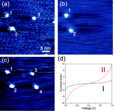 | ||
| Fig. 2 STM images of a typical information dots pattern and the corresponding I–V curves. (a) A triangular recording pattern composed of three information dots: pulsed voltage, +6.0 V; 2 ms. (b) Erasing one dot: pulsed voltage, −5.85 V; 4 ms. (c) Rewriting two information dots: pulsed voltage, +6.0 V; 2 ms. (d) Typical local current–voltage (I–V) curves in the unrecorded (curve I) and recorded region (curve II). | ||
To clarify the mechanism of the information dots formation, quantum chemical calculations are done using the hybrid Hartree–Fock/density functional theory (HF/DFT) method of B3LYP with the 6-31G* basis set (see details in the ESI†, Fig. S2). The charge density distributions of the HOMO and the LUMO are found to be intercepted at the central meta-conjugated truxene bridge. This can block the charge recombination at the ground state.26,27 By external pulsed voltage stimulus of the STM tips, the inelastic electron tunneling process transfers the energy of inelastic tunneling electrons to the component.38 The applied voltage pulse at the threshold can promote the CT process (Fig. S1b†) and switch the conductance of the recorded region from the OFF state to the ON state.39–41 It has been proved that the meta-conjugated bridge can enhance electronic coupling and the bridge would act as a wire to promote CT from donor to acceptor when at its excited state.26 Meanwhile, the meta-conjugated bridge can act like an insulator and prevent electronic communication in the recombination process without external stimulus.42 Resisting charge recombination in the reverse direction is important for the stability of the memory devices at the ON state.39,43–45 Effective recombination is blocked, which can lead to an asymmetric CT behavior and sustain the ON state. The charges are further delocalized to the conjugated thienylvinylene-TCF; thus the CT state can be more stable. The delocalized charges in the separate moieties hardly dissociate and the CT state in solid film can be stored until the application of a reverse bias.
The DBA compound is a photoactive molecule and its macroscopic memory device has photo-electrical responses to the UV light of 405 nm (Fig. S3 and S4†). The local I–V characteristics of the DBA thin film on HOPG are investigated under different light irradiations in Fig. 3. The tunneling current of the unrecorded film at the OFF state rises from 2.06 nA to 10.42 nA at 1 V, as the light power intensity increases from 0 to 2.13 mW cm−2 (Fig. 3a). The current increments of the recorded region (ON state) are more amplified than that of the unrecorded region (OFF state). The tunneling current of the recorded region at 1 V is 17.82 nA under dark conditions. When the UV light power rises to 1.12 mW cm−2, the tunneling current of the ON state is larger than 52 nA, which has already exceeded the measuring range of the instrument (Fig. 3b). The UV light can amplify the ON tunneling current more effectively than the OFF current, resulting in the amplification of the ON/OFF ratio. Fig. 3c calculates the ratio between the ON and OFF tunneling currents at 0.7 V. The ON/OFF ratio varies with the light intensities. All ON/OFF ratios under UV light are larger than the ratio under dark (4.1). The maximum ratio is up to 10.8 under the UV light of 1.12 mW cm−2.
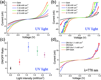 | ||
| Fig. 3 (a) Local I–V characteristics are examined under dark and different UV light illumination conditions before recording. (b) Local I–V characteristics of recorded regions show an obviously higher conductivity increment under various light intensity illuminations. (c) The fluctuation of ON/OFF ratio with different light power intensities shows that the film has the maximum ON/OFF ratio of 10.8 under the UV light power intensity of 1.12 mW cm−2. (d) The tunneling currents at ON and OFF states under visible light with the wavelength of 778 nm have a little change compared with that under dark conditions. | ||
STS of local I–V characteristics reveals the energy levels of frontier orbitals of molecules on a conductive substrate.46 The increment of resonant tunneling currents in STS could be originated from light-induced CT and consequently the effective reduction of the tunneling barrier height.47 The light wavelength is crucial. Visible light at the wavelength of 778 nm, which is far from the absorbance bands of the DBA compound, cannot effectively initiate the CT. The visible light was set at 1.1 mW cm−2, which is the optimal power intensity of the previous UV light. In Fig. 3d, both the ON and OFF current curves have negligible increments compared with that in the dark. Thus the local I–V characteristics changes arose from the photoelectric effect on the DBA molecule, rather than the thermodynamic effect of the light. Such amplification on ON/OFF ratios with UV light has shown to be power-dependent and wavelength-selective. This can provide a feasible method to modify the contrast of the STM images and consequently realize reversible nanoscale data storage readout in the following experiment.
To better explore the photo-induced amplification on the STM image contrast, the electronic coupling between the tip and the molecule on the substrate has been analyzed. The tunneling probability of electrons between the STM tip and the molecular states is largely determined by the effective tunneling barrier height and the barrier width. It can be demonstrated in the simplest form:
 | (1) |
 | ||
| Fig. 4 (a) A sequence of constant current mode STM images of the same specific region with various bias voltages (BV) from +0.9 V to +0.1 V. Insets 1–5 are scanned under dark condition. STM image is vaguer in contrast to the background and the information dots can barely be identified until the positive BV is lower than 0.5 V. Insets 6–10 are scanned under the UV light of 1.1 mW cm−2. The information dots could be visibly identified from the background in the whole scanning BV range from +0.9 V to +0.1 V. (b) The BV dependences of the tunneling current of the information dots and unrecorded area under dark and UV illumination are compared. (c) When the BV is smaller than +0.5 V, the tunneling current ratio between UV and dark (UV/dark ratio) at the recorded region could sustain higher than 1.8. (d) The ON/OFF ratios under UV and dark condition are compared. The UV light gives rise to about two times amplification of the ON/OFF ratio compared with dark condition in the whole scanning BV range. | ||
The BV-dependent tunneling current of the recorded and unrecorded areas under dark and UV illumination are compared in Fig. 4b. The STM images were scanned under the constant current mode. The feedback system of the equipment adapted to keeping the background tunneling current constant regardless of what the BV value was. In storage STM images, the recorded regions were small dots scattered on the large unrecorded areas. Unrecorded areas could represent the background of the STM image. The tunneling current of the unrecorded area had little change with the increase of BV. But the tunneling currents of the recorded regions dramatically decreased with the increase of BV. The tunneling current in the dark decreased from 22.0 pA to 7.6 pA, as the BV rose from +0.1 V to +0.9 V. With the UV light, the tunneling current was 44.5 pA at the BV of +0.1 V. At the BV of +0.9 V, the tunneling current under UV light was 10.2 pA. The interaction between the tip and the sample surface could be greatly strengthened under UV light and the values of the tunneling current were enhanced. The ratios of the tunneling current of the recorded dots region under UV and dark conditions are compared in Fig. 4c. When the BV is smaller than +0.5 V, the tunneling current ratio between UV and dark (UV/Dark Ratio) at the recorded region could sustain higher than 1.8.
The UV light increases the value of the tunneling current at the recorded area. This is ascribed to the light-induced CT and consequently the effective reduction of the tunneling barrier height.48 The effective barrier height normally depends on the work functions of the tip and sample.47 According to the quasi-resonant tunneling model,15,46 the molecular orbital that is closer in energy to the Fermi level of the electron source affects the tunneling process more strongly. Electrons tunnel from the HOPG at the positive voltage bias of STM under air conditions. In the absence of UV light, the HOMO state of the compound is expected to be closer to the Fermi level of HOPG than to the other energy states. UV light irradiation can excite photo-induced electrons into higher orbitals.32 The observed band gap could be estimated from the onset of the absorption at the low-energy edge of the solid film absorption peaks. The observed band gap of the DBA molecules (1.59 eV) is larger than the calculated HOMO–LUMO gaps from cyclic voltammetry (1.1 eV) (see ESI†, Fig. S2, S5 and S6). There are more transitions besides the direct transition from the HOMO to the LUMO. The excess energy can excite photo-induced electrons into the LUMO + 1 and higher orbitals and open additional electron transfer channels, which increases the tunneling probability. Therefore the photoelectric effect could improve the tunneling current, and result in amplifying the UV/dark ratio (Fig. 4c).
The above results show that UV light and BV are two factors that can affect the tunneling current. The tunneling current reflects the tunneling probability of electrons between the STM tip and the molecules at one point. The contrast of STM image shows the whole spatial electron-tunneling distributions of the scanning area.15,52,53 The contrast enhancement of the STM storage image is arisen from the larger ON/OFF ratio of the tunneling current under UV light (Fig. 4d). The CT state of the DBA molecule in the recorded region occupies molecular orbital with higher energy levels than the ground state of the DBA molecule at the unrecorded region. The plausible occupied electronic states become denser as the energy levels increase.47,54Photon-excited electrons can find more resonant molecular states to tunnel. Therefore, the recorded dot region has higher tunneling probability of photon-excited electrons than the unrecorded region, when under UV light irradiation. The ON tunneling currents are more effectively amplified than the OFF currents, resulting in the amplification of the ON/OFF ratio. The maximum ON/OFF ratio under UV light is 12.5 at a BV of 0.2 V. The maximum ON/OFF ratio under the dark is 7 at a BV of 0.2 V which is even lower than the ON/OFF ratio under UV light at a BV of 0.4 V. Compared with dark condition, the UV light can give rise to about two times amplification of the ON/OFF ratio in the whole scanning BV range.
Contrast amplification of the STM storage image
By optimizing scanning parameters of the STM instrument, the readout contrast of the STM image containing information patterns can be reversibly modified (Fig. 5a and b). Region I is a selected control area of the bare HOPG substrate, where the organic molecule layer is broken down by high voltage pulse (10 V, 10 ms). Regions II and III are two pairs of information dots obtained by applying the proper pulsed voltage (5–6 V, 2 ms). In Fig. 5a, the STM image is vague in contrast and the information dots are obscured from the background under the dark. Applying the UV light with the power intensity of 1.1 mW cm−2 (Fig. 5b), the contrast of the STM image can be largely enhanced without changing other scanning parameters. The information dots which cannot be identified in the usual dark scanning condition can be clearly read out through the photo-induced amplification effect. | ||
| Fig. 5 Modifying the scanning parameters can obtain different contrast of STM images. (a) The readout contrast of the STM recording image is low under the dark condition. The information dots at regions II and III were obscured among the background. (b) Applying the UV light, the readout contrast of the STM image was enhanced and the information dots could be clearly identified from the background. (c) The tunneling current profiles of the STM image under dark and UV light illumination are compared. | ||
In Fig. 5c, the tunneling current profiles of the STM image under dark and UV light illumination are analyzed. Region I was served as the control in the scanning. The tunneling current profiles across region I show no distinct change with or without the UV light. It has no response to the light. The maximum tunneling current peak is larger than 400 pA at region I. These indicate that region I is a bare graphite substrate area which is much more conductive than other regions covered with organic molecules. The tunneling current profiles across regions II and III (Fig. 5c) show that there exist small picks around the information dots. But the contrast is not sufficient between the current peak of the information dots and the background current fluctuation. So the information dots cannot be identified in recorded regions II and III in the STM image when scanned in the dark (Fig. 5a). Under UV irradiation, the tunneling current peak increases from the 43.9 pA to 117.6 pA at recorded region II, and from the 41.6 pA to 100.8 pA at region III. The contrast of the information dots scanned under the UV light is enhanced more than two times, therefore the information dots could be brighter and clearer to be visualized in the STM recording image (Fig. 5b).
Conclusions
In summary, a strategy to enhance the readout contrast has been achieved through the photo-induced amplification effect in STM nanoscale data storage. A DBAmeta-conjugated compound was designed and applied as the storage medium. Reversible recording dots with an average diameter of 2 nm were realized. The conductance of the DBA compound could be affected by its photoactive property, leading to a photo-induced amplification effect. This effect improved the tunneling current at the ON state much more than that at the OFF state, resulting in about two times amplification of the ON/OFF ratio and a contrast enhancement of the STM storage image in the readout process. The photo-induced amplification effect has shown wavelength-selective and light power-dependent characteristics. These results suggested a new approach to designing efficient memory materials and devices.Acknowledgements
The authors thank Dr Jianming Chen and Dr Liu Yang for helpful discussions. This work is supported by the National Nature Science Foundation (Grant Nos.21003132, 21073203, 21004068, 61001051, 91127038, 51103004 and 51173190), and the 973 Program (2007CB936403, 2009CB930404, 2011CB932303 and 2011CB808400).Notes and references
- R. Chau, B. Doyle, S. Datta, J. Kavalieros and K. Zhang, Nat. Mater., 2007, 6, 810–812 CrossRef CAS.
- X. Ma and H. Tian, Chem. Soc. Rev., 2010, 39, 70–80 RSC.
- H. Tian, Angew. Chem., Int. Ed., 2010, 49, 4710–4712 CAS.
- M. R. Stan, P. D. Franzon, S. C. Goldstein, J. C. Lach and M. M. Ziegler, Proc. IEEE, 2003, 91, 1940–1957 CrossRef CAS.
- Y. Chen, G. Y. Jung, D. A. A. Ohlberg, X. M. Li, D. R. Stewart, J. O. Jeppesen, K. A. Nielsen, J. F. Stoddart and R. S. Williams, Nanotechnology, 2003, 14, 462–468 CrossRef CAS.
- S. Moller, C. Perlov, W. Jackson, C. Taussig and S. R. Forrest, Nature, 2003, 426, 166–169 CrossRef.
- Q. D. Ling, F. C. Chang, Y. Song, C. X. Zhu, D. J. Liaw, D. S. H. Chan, E. T. Kang and K. G. Neoh, J. Am. Chem. Soc., 2006, 128, 8732–8733 CrossRef CAS.
- P. Vettiger, G. Cross, M. Despont, U. Drechsler, U. Durig, B. Gotsmann, W. Haberle, M. A. Lantz, H. E. Rothuizen, R. Stutz and G. K. Binnig, IEEE Trans. Nanotechnol., 2002, 1, 39–55 CrossRef.
- H. J. Mamin, B. D. Terris, L. S. Fan, S. Hoen, R. C. Barrett and D. Rugar, IBM J. Res. Dev., 1995, 39, 681–699 CrossRef CAS.
- D. M. Eigler and E. K. Schweizer, Nature, 1990, 344, 524–526 CrossRef CAS.
- A. Sato and Y. Tsukamoto, Nature, 1993, 363, 431–432 CrossRef.
- H. M. Wu, Y. L. Song, S. X. Du, H. W. Liu, H. J. Gao, L. Jiang and D. B. Zhu, Adv. Mater., 2003, 15, 1925–1929 CrossRef CAS.
- H. J. Gao, K. Sohlberg, Z. Q. Xue, H. Y. Chen, S. M. Hou, L. P. Ma, X. W. Fang, S. J. Pang and S. J. Pennycook, Phys. Rev. Lett., 2000, 84, 1780–1783 CrossRef CAS.
- H. J. Gao and L. Gao, Prog. Surf. Sci., 2010, 85, 28–91 CrossRef CAS.
- A. Miura, Z. J. Chen, H. Uji-i, S. De Feyter, M. Zdanowska, P. Jonkheijm, A. Schenning, E. W. Meijer, F. Wurthner and F. C. De Schryver, J. Am. Chem. Soc., 2003, 125, 14968–14969 CrossRef CAS.
- A. Bandyopadhyay and A. J. Pal, J. Phys. Chem. B, 2003, 107, 2531–2536 CrossRef.
- S. Sahu and A. J. Pal, Org. Electron., 2008, 9, 873–877 CrossRef.
- Y. Ma, X. B. Cao, G. Li, Y. Q. Wen, Y. Yang, J. X. Wang, S. X. Du, L. M. Yang, H. J. Gao and Y. L. Song, Adv. Funct. Mater., 2010, 20, 803–810 CrossRef CAS.
- Y. Q. Wen, J. X. Wang, J. P. Hu, L. Jiang, H. J. Gao, Y. L. Song and D. B. Zhu, Adv. Mater., 2006, 18, 1983–1987 CrossRef CAS.
- Y. L. Shang, Y. Q. Wen, S. L. Li, S. X. Du, X. B. He, L. Cai, Y. F. Li, L. M. Yang, H. J. Gao and Y. L. Song, J. Am. Chem. Soc., 2007, 129, 11674–11675 CrossRef CAS.
- M. Feng, L. Gao, Z. T. Deng, W. Ji, X. F. Guo, S. X. Du, D. X. Shi, D. Q. Zhang, D. B. Zhu and H. J. Gao, J. Am. Chem. Soc., 2007, 129, 2204 CrossRef CAS.
- A. Bandyopadhyay, A. Chowdhury and A. J. Pal, Opt. Mater., 2006, 28, 1432–1436 CrossRef CAS.
- J. Chen, M. A. Reed, A. M. Rawlett and J. M. Tour, Science, 1999, 286, 1550–1552 CrossRef CAS.
- J. E. Green, J. W. Choi, A. Boukai, Y. Bunimovich, E. Johnston-Halperin, E. DeIonno, Y. Luo, B. A. Sheriff, K. Xu, Y. S. Shin, H. R. Tseng, J. F. Stoddart and J. R. Heath, Nature, 2007, 445, 414–417 CrossRef CAS.
- Z. J. Donhauser, B. A. Mantooth, K. F. Kelly, L. A. Bumm, J. D. Monnell, J. J. Stapleton, D. W. Price, A. M. Rawlett, D. L. Allara, J. M. Tour and P. S. Weiss, Science, 2001, 292, 2303–2307 CrossRef CAS.
- A. L. Thompson, T. S. Ahn, K. R. J. Thomas, S. Thayumanavan, T. J. Martinez and C. J. Bardeen, J. Am. Chem. Soc., 2005, 127, 16348–16349 CrossRef CAS.
- K. M. Gaab, A. L. Thompson, J. J. Xu, T. J. Martinez and C. J. Bardeen, J. Am. Chem. Soc., 2003, 125, 9288–9289 CrossRef CAS.
- D. Gust, T. A. Moore and A. L. Moore, Acc. Chem. Res., 2001, 34, 40–48 CrossRef CAS.
- M. R. Wasielewski, Chem. Rev., 1992, 92, 435–461 CrossRef CAS.
- C. H. Duan, K. S. Chen, F. Huang, H. L. Yip, S. J. Liu, J. Zhang, A. K. Y. Jen and Y. Cao, Chem. Mater., 2010, 22, 6444–6452 CrossRef CAS.
- Y. Y. Noh, J. Ghim, S. J. Kang, K. J. Baeg, D. Y. Kim and K. Yase, J. Appl. Phys., 2006, 100, 094501 CrossRef.
- E. Varene, I. Martin and P. Tegeder, J. Phys. Chem. Lett., 2011, 2, 252–256 CrossRef CAS.
- J. Borghetti, V. Derycke, S. Lenfant, P. Chenevier, A. Filoramo, M. Goffman, D. Vuillaume and J. P. Bourgoin, Adv. Mater., 2006, 18, 2535–2540 CrossRef CAS.
- Y. Y. Noh, D. Y. Kim, Y. Yoshida, K. Yase, B. J. Jung, E. Lim and H. K. Shim, Appl. Phys. Lett., 2005, 86, 043501 CrossRef.
- Y. Ma, Y. Q. Wen, J. X. Wang, Y. L. Shang, S. X. Du, L. D. Pan, G. Li, L. M. Yang, H. J. Gao and Y. L. Song, J. Phys. Chem. C, 2009, 113, 8548–8552 CAS.
- Z. M. Tang, T. Lei, J. L. Wang, Y. G. Ma and J. Pei, J. Org. Chem., 2010, 75, 3644–3655 CrossRef CAS.
- J. S. Yang, H. H. Huang and J. H. Ho, J. Phys. Chem. B, 2008, 112, 8871–8878 CrossRef CAS.
- M. Feng, L. Gao, S. X. Du, Z. T. Deng, Z. H. Cheng, W. Ji, D. Q. Zhang, X. F. Guo, X. Lin, L. F. Chi, D. B. Zhu, H. Fuchs and H. J. Gao, Adv. Funct. Mater., 2007, 17, 770–776 CrossRef CAS.
- C. W. Chu, J. Ouyang, H. H. Tseng and Y. Yang, Adv. Mater., 2005, 17, 1440–1443 CrossRef CAS.
- Q. D. Ling, Y. Song, S. L. Lim, E. Y. H. Teo, Y. P. Tan, C. X. Zhu, D. S. H. Chan, D. L. Kwong, E. T. Kang and K. G. Neoh, Angew. Chem., Int. Ed., 2006, 45, 2947–2951 CrossRef CAS.
- Q. D. Ling, S. L. Lim, Y. Song, C. X. Zhu, D. S. H. Chan, E. T. Kang and K. G. Neoh, Langmuir, 2007, 23, 312–319 CrossRef CAS.
- J. P. Hu, Y. F. Li, Z. Y. Ji, G. Y. Jiang, L. M. Yang, W. P. Hu, H. J. Gao, L. Jiang, Y. Q. Wen, Y. L. Song and D. B. Zhu, J. Mater. Chem., 2007, 17, 3530 RSC.
- A. M. Scott and M. R. Wasielewski, J. Am. Chem. Soc., 2011, 133, 3005–3013 CrossRef CAS.
- J. Y. Ouyang, C. W. Chu, C. R. Szmanda, L. P. Ma and Y. Yang, Nat. Mater., 2004, 3, 918–922 CrossRef CAS.
- L. P. Ma, J. Liu and Y. Yang, Appl. Phys. Lett., 2002, 80, 2997–2999 CrossRef CAS.
- H. Uji-i, A. Miura, A. Schenning, E. W. Meijer, Z. J. Chen, F. Wurthner, F. C. De Schryver, M. Van der Auweraer and S. De Feyter, ChemPhysChem, 2005, 6, 2389–2395 CrossRef CAS.
- S. W. Wu and W. Ho, Phys. Rev. B: Condens. Matter Mater. Phys., 2010, 82, 085444 CrossRef.
- C. L. Claypool, F. Faglioni, W. A. Goddard, H. B. Gray, N. S. Lewis and R. A. Marcus, J. Phys. Chem. B, 1997, 101, 5978–5995 CrossRef CAS.
- J. Tersoff and D. R. Hamann, Phys. Rev. Lett., 1983, 50, 1998–2001 CrossRef CAS.
- J. Tersoff and D. R. Hamann, Phys. Rev. B, 1985, 31, 805–813 CrossRef CAS.
- J. Tersoff, Phys. Rev. B, 1989, 40, 11990–11993 CrossRef.
- A. Weber-Bargioni, W. Auwarter, F. Klappenberger, J. Reichert, S. Lefrancois, T. Strunskus, C. Woll, A. Schiffrin, Y. Pennec and J. V. Barth, ChemPhysChem, 2008, 9, 89–94 CrossRef CAS.
- D. Wang, Q. Chen and L. J. Wan, Phys. Chem. Chem. Phys., 2008, 10, 6467–6478 RSC.
- R. L. McCreery, Chem. Mater., 2004, 16, 4477–4496 CrossRef CAS.
Footnote |
| † Electronic supplementary information (ESI) available: Absorption spectrum of DBA molecule; computational details and molecular orbitals; photoelectric cooperation on bistable electrical performance of macroscopic devices; energy levels calculated from the experiments. See DOI: 10.1039/c2jm14923k |
| This journal is © The Royal Society of Chemistry 2012 |