Optimization of photoelectrochemical water splitting performance on hierarchical TiO2 nanotube arrays†
Received
14th December 2011
, Accepted 9th February 2012
First published on 10th February 2012
Abstract
In this paper, we show that by varying the voltages during two-step anodization the morphology of the hierarchical top-layer/bottom-tube TiO2 (TiO2 NTs) can be finely tuned between nanoring/nanotube, nanopore/nanotube, and nanohole–nanocave/nanotube morphologies. This allows us to optimize the photoelectrochemical (PEC) water splitting performance on the hierarchical TiO2 NTs. The optimized photocurrent density and photoconversion efficiency in this study, occurring on the nanopore/nanotube TiO2 NTs, were 1.59 mA cm−2 at 1.23 V vs. RHE and 0.84% respectively, which are the highest values ever reported on pristine TiO2 materials under illumination of AM 1.5G. Our findings contribute to further improvement of the energy conversion efficiency of TiO2-based devices.
Broader content
The present annual worldwide energy consumption is ∼15 TW and is expected to reach 30 TW by 2050. Moreover, due to stock limitation, energy supply from non-renewable fossil fuels, such as oil, coal, natural gas, is shrinking. In view of this, generation of clean and renewable energy has drawn significant interest from academia and industry. Solar light is without any doubt the most renewable energy source available to us. The collection, conversion and storage of solar energy are three key processes for practical applications and these processes can all be integrated in a single monolithic photoelectrochemical (PEC) water splitting cell. Within it the solar energy is converted and contained in hydrogen gas, which is considered as “new oil” in the future. In this study, hierarchical TiO2 nanotube (TiO2 NT) arrays, widely regarded as promising candidates for enhancing solar energy efficiency in PEC cells, were prepared by two-step anodization for PEC water splitting applications. We show that simple, controllable, and rational modulation of morphology, optical absorption and crystallinity of the hierarchical TiO2 NTs can remarkably boost their water splitting performance. Our findings contribute to further improvement of the energy conversion efficiency of TiO2-based devices.
|
Introduction
Solar light is the most abundant energy source and the solar energy that strikes the earth in a day is more than the total energy consumption of the world in a year.1 Solar energy collection, conversion and storage are three key processes for practical applications and these processes can all be integrated in a single monolithic photoelectrochemical (PEC) water splitting cell, within which the solar energy is converted and contained in the simplest chemical bond, H–H.2 The PEC cells are typically designed with metal oxide semiconductors as photoelectrodes and noble metals as counter electrodes. Among the metal oxide semiconductors being intensively investigated (e.g., TiO2,3,4 ZnO,5,6 Fe2O3,7,8 WO3,9 and Cu2O10), TiO2 distinguishes itself due to its favorable band-edge positions, superior chemical and optical stability, and low cost. However, due to two fundamental reasons, the photoconversion efficiency and photocurrent density of TiO2 based photoanodes are still not satisfactory. First, the large band gap of TiO2 (i.e., 3.2 eV for anatase and 3.0 eV for rutile) limits its optical absorption within the UV light region; second, a general mismatch between the optical path length required for high light absorption (at least 1 μm for 90% light absorption) and the optimal charge diffusion length (usually 70 nm for the minority carrier: hole) leads to fast photoelectron–hole recombination in powder TiO2 based PEC cells.11–13 Sensitization with small band gap semiconductors/dyes and non-metal doping are among the most investigated approaches for expanding the TiO2 optical absorption spectrum into the visible and infrared regions.14 Due to the high level of control over their aspect ratio, one-dimensional nanostructures of semiconductors, such as nanotubes (NTs), nanorods, and nanowires, permit optimization of the optical path length and charge diffusion length relatively independently and they are thus regarded as promising candidates to solve the issue of mismatch between optical path and charge diffusion lengths.15,16 In particular, TiO2 NTs arrays prepared in anodization processes have recently attracted considerable research attention owing to their facile preparation procedure, high surface area for contact with the supporting electrolyte, high light harvesting efficiency enhanced by light scattering, and high electron mobility induced by their one-dimensional nanostructure.17,18 Normally, TiO2 NTs fabricated in conventional one-step anodization processes suffer from disparity in tube lengths and considerable tube array surface roughness. A two-step anodization process, which is composed of the first anodization for growth of TiO2 NTs and their subsequent removal and the second anodization to grow TiO2 NTs from the same substrate, is an alternative for the preparation of much more uniform TiO2 NT arrays.19,20 Moreover, under suitable synthesis conditions, unique hierarchical top-layer/bottom-tube TiO2 NT arrays can be fabricated, which have been proven to possess significantly better performance in dye sensitized solar cells than those fabricated using the conventional one-step anodization.21 Furthermore, it is possible that with suitable morphology, the top-layer can serve as a photonic crystal to enhance the optical absorption of the hierarchical TiO2 NTs. However, there are only a few reports available in the literature examining PEC performances with hierarchical TiO2 NTs based photoelectrodes.22,23
The objective of this study is to optimize the PEC water splitting performance of the hierarchical top-layer/bottom-tube TiO2 NTs photoanodes, which can be achieved by adjusting the voltages applied in the two anodization steps (Scheme 1). The key contribution of the present study is that we show by applying a simple fabrication strategy the photocurrent density and photoconversion efficiency of the hierarchical TiO2 NTs can be remarkably boosted. As a matter of fact, the optimal photocurrent density and photoconversion efficiency of the hierarchical TiO2 NTs in our system were 1.59 mA cm−2 and 0.84%, the highest values ever reported for single component TiO2 materials.
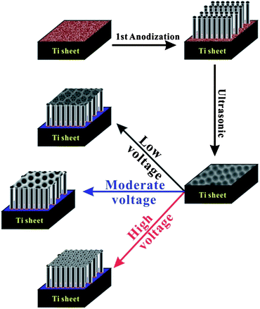 |
| | Scheme 1 Two-step anodization synthesis of the hierarchical TiO2 NTs. | |
Experimental
Chemicals and materials
A 2 mm thick titanium sheet (99.6%, Strem Chemicals) was cut into pieces of 25 × 10 mm2. Ethylene glycol (EG), ammonia fluoride (NH4F), potassium hydroxide (KOH) were purchased from Acros Organics and used as received. All aqueous solutions were prepared using deionized (DI) water with a resistivity of 18.2 MΩ cm that was prepared by a Millipore system.
Preparation of TiO2 NTs
The TiO2 NTs were fabricated by a two-step anodization process. Prior to anodization, the Ti sheets were first degreased by sonicating in ethanol and room-temperature DI water, followed by drying in a pure nitrogen stream. The anodization was carried out using a conventional two-electrode system with the Ti sheet as an anode and a Pt gauze (Aldrich, 100 mesh) as a cathode. All electrolytes consisted of 0.5 wt% NH4F in EG solution with 2 vol% water. All anodizations were carried out at room temperature. In the first-step anodization, the Ti sheet was anodized at 60, 80, or 100 V for 60 min, and then the as-grown nanotube layer was ultrasonically removed in DI water. The same Ti sheet then underwent the second anodization at different potentials in range of 20–100 V with tunable duration to control the thickness of the NTs. After the two-step anodization, the prepared TiO2 NT samples were cleaned with DI water and dried with N2 gas. The anodized TiO2 NTs were annealed in air at 450 °C for 1 h with a heating rate of 5 °C min−1.
Characterization of TiO2 NTs
The morphology of the hierarchical TiO2 NTs was determined by field-emission scanning electron microscope (FESEM, FEI Quanta 600). The crystalline structure was analyzed by X-ray diffraction (XRD, Bruker D8 Discover diffractometer, using Cu Kα radiation, λ = 1.540598 Å). The diffuse reflectance UV–vis adsorption spectra were recorded on spectrophotometer (Shimadazu, UV 2550), with fine BaSO4 powder as a reference.
Photoelectrochemical characterization of TiO2 NTs
The photoelectrochemical performance of the TiO2 NTs was evaluated using a three-electrode configuration with a TiO2 NTs electrode, Ag/AgCl electrode, and Pt mesh as the working, reference and counter electrode, respectively. The supporting electrolyte was 1 M KOH solution. The potential and photocurrent of the photoelectrode were controlled by a potentiostat and were reported against the reversible hydrogen electrode (RHE) following the equation below:| | | ERHE = EAg/AgCl + 0.059pH + E°Ag/AgCl with E°Ag/AgCl = 0.1976 V at 25 °C | (1) |
The scan rate for the linear sweep voltammetry was 5 mV s−1. The photoresponse was evaluated under chopped light irradiation (light on/off cycles: 60 s) at a fixed electrode potential of 1.23 V vs. RHE. The photocurrent was measured under irradiation from a 300 W Xe lamp (PLS-SXE300, PE300BF). The intensity of the light source was calibrated with a Si diode (Model 818, Newport) to simulate AM 1.5 illumination (100 mW cm−2). The electrochemical impedance spectra (EIS) were measured using a PGSTAT302N Autolab Potentiostat/Galvanostat (Metrohm) equipped with a frequency analyzer module (FRA2) with an excitation signal of 10 mV amplitude. The impedance vs. frequency spectra were acquired at the open circular potential of the system under the illumination conditions. Afterward, impedance vs. potential measurements at a fixed frequency were performed to determine the carrier density.
Results and discussion
As shown in Scheme 1, to prepare the hierarchical TiO2 NTs, a Ti sheet was first anodized under certain voltage to grow TiO2 NTs on its surface. The TiO2 NTs (Fig. S1a, ESI†) were subsequently removed by ultrasonication, leaving behind on the Ti sheet surface a regular hexagonally packed round concave morphology (Fig. 1d4, Fig. S1b, ESI†). The pattered Ti sheet was then subject to the second anodization to yield uniform TiO2 NTs with unique hierarchical top-layer/bottom-tube nanostructures. It is generally believed that the growth of porous or tubular anodic metal oxide films, such as alumina and titania, is an outcome of the competition between the electric field driven oxidation of metal (υelectro) to form oxides, and the electric field assisted and chemical dissolution of the metal oxide layer (υdis).24 With the existence of fluoride anions as electrolytes in the hierarchical TiO2 NT synthesis system, the dissolution of titania in the form of [TiF6]2− is greatly affected by the applied electric field. Thus, it is reasonable to believe that the density of the electric field applied during anodization significantly affects the morphology of the hierarchical TiO2 NT arrays. In this study three different voltages (i.e., 60, 80, or 100 V) were applied in the first anodization step for fast patterning of the sheet and convenient removal of the tubes by ultrasonication, and five voltages (i.e., 20, 40, 60, 80, 100V) were employed in the second anodization step. The samples were denoted by S-x-y with x and y being the anodization voltage in the first and second anodization steps respectively.
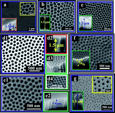 |
| | Fig. 1 SEM images of (a) S-60-20; top right inset shows a high magnification image and bottom left inset shows cross-sectional view with a length of the TiO2 NTs of 1.3 μm; (b) S-60-40; inset shows cross-sectional view with a length of 1.5 μm; (c) S-60-60; inset shows cross-sectional view with a length of 1.3 μm; (d1) S-60-80; (d2) cross-sectional view of S-60-80 with a length of 1.5 μm, (d3) 15° cross-sectional view of S-60-80; (d4) regular hexagonally packed pattern with round concave morphology on a Ti sheet surface after ultrasonic removal of the NTs layer; (e1) S-60-100; (e2) cross-sectional view of S-60-100 with a length of 1.4 μm; (f) S-80-80; inset shows cross-sectional view with a length of 1.4 μm; (g) S-100-80; top right inset shows high magnification image, and bottom left inset shows cross-sectional view with a length of 1.5 μm. | |
Fig. 1a through 1e present scanning electron microscopy (SEM) images of the hierarchical TiO2 NTs prepared at different voltages in the second anodization, with the first anodization voltage fixed at 60 V. We denote the morphology of the hierarchical TiO2 NTs samples synthesized at 20 and 40 V (i.e., S-60-20 and S-60-40) as nanoring/nanotube and that at 60, 80 and 100 V (i.e., S-60-60, S-60-80, and S-60-100) as nanopore/nanotube (Fig. 1). With increasing density of the applied electric field, υelectro increases, whereas υdis decreases due to coulomb force on the [TiF6]2− anion. Thus, at the low voltages of 20 and 40 V in the second anodization, and presumably due to the relatively high υdis, relatively little accumulation/deposition of Ti(OH)4 occurred at the openings of the NTs where the NTs met the bulk electrolyte, resulting in the formation of the unique nanoring/nanotube hierarchical nanostructures (i.e., S-60-20 and S-60-40) (Fig. 1a–b). As the anodization voltage increases further, accumulation/deposition of Ti(OH)4 at the entrance of the NTs increases correspondingly. This leads to the sequential formation of nanopore and nanohole top structures, with the diameters of the openings decreasing with increasing voltages. On the other hand, as an increase in υelectro favors the formation of a thicker oxide layer, at high anodization voltages the applied electric field tends to preferentially focus on the bottom of the concavity generated in the first-step anodization where the electrical resistance is the lowest. As a result, the diameters of the bottom tubes of S-60-60, S-60-80, and S-60-100 increase with increasing voltages, which agrees well with the literature.25,26 To investigate the effect of the voltage in the first anodization step, S-60-80 was compared with S-80-80 and S-100-80. As shown in Fig. 1f and 1g, S-80-80 revealed similar nanopore/nanotube structures to S-60-100 whereas S-100-80 exhibited a unique top morphology, which is denoted as a nanohole–nanocave/nanotube structure. As clearly shown in Fig. 1g, the top of the nanohole–nanocave/nanotube structure consists of holes with a pore size of around 50 nm and concaves with closed bottoms. The distinctly different morphology of S-100-80 may be due to the formation of a thick oxide barrier layer in the first anodization step at the high voltage (i.e., 100 V). As shown in the insets in Fig. 1, all samples were precisely controlled with a uniform length of TiO2 NTs in the range of 1.3–1.5 μm, for the purpose of minimizing the effect of tube length disparity on PEC performance.
Linear sweep photovoltammetry measurements were performed to determine the photocurrent densities of different samples using a three-electrode electrochemical system in a 1 M KOH electrolyte under AM 1.5G (100 mW cm−2) illumination. Analysis of the photocurrent densities on different samples (Fig. 2a) allows us to draw the following three major conclusions. (1) All samples prepared by the two-step anodization method showed consistently higher photocurrent densities under the same conditions (Fig. 2a) than ones prepared by the conventional one-step method (anodization with 80 V), implying that the hierarchical TiO2 nanostructures favor better PEC performances. The photocurrent density of the TiO2 NTs photoanode prepared by the conventional one-step anodization method was only 0.345 mA cm−2 at 0.23 V vs. Ag/AgCl or 1.23 V vs. RHE, which is the potential often chosen as a metric to evaluate the performance of photoanodes as it corresponds to the water oxidation potential. S-60-80, among all samples, generated the highest photocurrent density of 1.59 mA cm−2 at the same potential, which is also the highest photocurrent density value ever reported on pristine TiO2 materials under illumination of AM 1.5G. It is worth mentioning that it is not our intention to compare the PEC water splitting performance of our system (i.e., single-component TiO2) with those involving extra chemical addition/modifications (e.g., ion intercalation, hydrogenation, noble metal deposition, sensitization). (2) The photocurrent densities (I) of different samples showed a general order of Inanopore/nanotube > Inanoring/nanotube > Inanohole–nanocave/nanotube. The nanohole–nanocave/nanotube sample (i.e., S-100-80) showed a relatively low photocurrent density (0.480 mA cm−2), supposedly due to the closed nanocave structures on its surface which effectively blocks the light absorption and solution infiltration. On the other hand, the nanopore/nanotube samples (i.e., S-60-60, S-60-80, and S-60-100) showed higher photocurrent densities than the nanoring/nanotube samples (i.e., S-60-20 and S-60-40), which is due to the formers' better degree of crystallinity and high optical absorption (to be discussed in a later section). (3) Among all of the nanopore/nanotube samples, S-60-80, the one with improved uniformity, showed the highest photocurrent density, which is due to its better optical absorption. In addition, a uniform morphology reduces structure defects which would otherwise serve as photoelectron/hole recombination centers, and thus favors high PEC performance. The photoconversion (i.e., photon-to-hydrogen) efficiency of the hierarchical TiO2 samples was calculated using the following equation:27
| | | η (%) = I(E°rev − V)/Jlight | (2) |
where
η is the photoconversion efficiency,
I is the photocurrent density (mA cm
−2),
Jlight is the incident light irradiance (mW cm
−2),
E°
rev is the standard reversible potential which is 1.23 V
vs. RHE, and V is the applied bias potential
vs. RHE.
Fig. 2b presents the plots of the photoconversion efficiency
vs. applied bias potentials. Among all of the samples, the TiO
2 NTs photoanode prepared by the conventional one-step
anodization method showed the lowest optimal photoconversion efficiency of 0.15% while S-60-80 exhibited the highest optimal photoconversion efficiency of 0.84%, which, to our best knowledge, is also the highest photoconversion efficiency of pristine TiO
2 materials ever reported under illumination of AM 1.5G. The photoconversion efficiency of all two-step samples were all greater than 0.31%, at least two times higher than that of the one-step sample. The photocurrent densities and photoconversion efficiencies of all samples are summarized in
Table 1. Amperometric
I–
t measurements were also performed to examine the photoresponse of the hierarchical TiO
2 NTs over time (
Fig. 2c), and fast photoresponses were recorded for all samples under conditions of alternating light on and light off and this photocurrent pattern was highly reproducible for many on/off cycles.
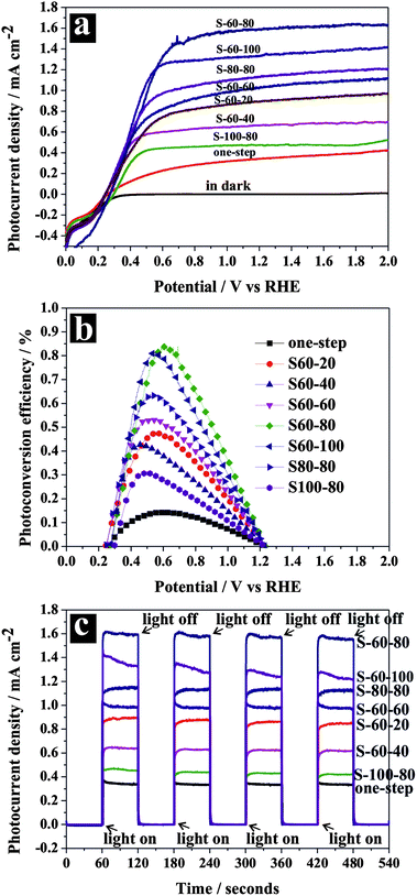 |
| | Fig. 2 Photoelectrochemical properties of hierarchical TiO2 NTs electrodes: (a) linear-sweep voltammograms collected with a scan rate of 5 mV s−1 in the dark and under illumination; (b) photoconversion efficiency as a function of the applied potential; (c) amperometric I–t curves at an applied potential of 1.23 V vs. RHE under illumination with 60 s light on/off cycles. | |
Table 1 Summary of PEC performance of hierarchical TiO2 NTs
| Samples |
Current density at 1.23 V vs. RHE/mA cm−2 |
Photoconversion efficiency (%) |
Carrier density/cm−3 |
| One-step |
0.342 |
0.15 |
2.45 × 10¹⁹ |
| S-60-20 |
0.901 |
0.48 |
3.57 × 10¹⁹ |
| S-60-40 |
0.670 |
0.43 |
3.02 × 10¹⁹ |
| S-60-60 |
1.03 |
0.54 |
4.69 × 10¹⁹ |
| S-60-80 |
1.59 |
0.84 |
8.48 × 10¹⁹ |
| S-60-100 |
1.34 |
0.81 |
5.84 × 10¹⁹ |
| S-80-80 |
1.14 |
0.64 |
5.81 × 10¹⁹ |
| S-100-80 |
0.480 |
0.32 |
2.72 × 10¹⁹ |
Optical absorption and crystalline properties are two important factors for the PEC performance on TiO2 materials. A material with a better optical absorption and higher crystallinity will subsequently result in a better PEC performance. Therefore, diffuse reflectance UV–vis absorption spectra and XRD measurement were employed in this study to characterize the optical absorption properties and crystallinity of the hierarchical TiO2 NTs (Fig. 3). As shown in Fig. 3a (DRS UV–vis absorption spectra), all two-step hierarchical TiO2 NTs samples depicted better UV absorption than one-step TiO2 NTs sample due to their unique hierarchical nanostructures and also better morphological uniformity. A better surface morphological uniformity might indicate better periodicity of the photonic crystals formed by the top porous layers and thus a better optical absorption. Among the hierarchical TiO2 NT samples, those with better surface morphological uniformity, such as S-60-20, S-60-80, S-80-80, presented better optical absorption.
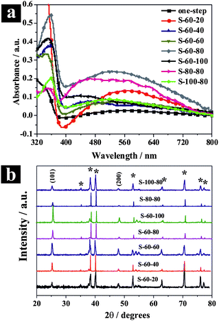 |
| | Fig. 3 (a) Diffuse reflectance UV–vis absorption spectra of the hierarchical TiO2 NTs. (b) XRD patterns of the hierarchical TiO2 NTs (the asterisk denotes Ti patterns). | |
The XRD patterns of the hierarchical TiO2 NTs after annealing in the same conditions (450 °C for 1 h in air) were shown in Fig. 3b. Clearly, all hierarchical TiO2 NTs samples formed pure crystalline anatase and showed a strong preferential orientation of (101). The average crystallite size of the samples was estimated using the Debye–Scherrer equation from the (101) crystal planes,28 and was used as a criterion to evaluate the degree of crystallinity of the samples (Fig. S2, ESI†). As is generally accepted, the crystallite size of TiO2 NTs increases with increasing voltages employed in anodization process.29 This can be explained by the fact that high voltage favors the formation of bigger crystal nucleus and thus results in a better crystallinity and less defects, with which our results agree well. In our case, with a fixed first anodization voltage of 60 V, at the second anodization voltages of 20, 40, 60, 80 and 100 V, the average crystallite size was 28, 29, 31, 34, and 43 nm respectively, increasing monotonically (Fig. S2, ESI†).
By comparing optical absorption properties and crystallinity of the hierarchical TiO2 NTs against their PEC performances (Fig. 2), we conclude that the optimal optical absorption properties and crystallinity of the hierarchical TiO2 NTs cannot be achieved simultaneously. For example, S-60-20 did not show a high photocurrent density even though it had a good optical absorbance in the UV region because its low crystallinity was the limiting factor; S-60-100 failed to generate the highest photocurrent density even though it possessed the best crystallinity among all of the samples because its relatively low optical absorbance limited its performance in this case. Among all samples, S-60-80 showed the highest PEC performance, which was due to a suitable combination of its good light absorption and crystallinity.
To better understand the enhanced PEC performance, the inherent electronic properties of the hierarchical TiO2 NTs were characterized by measuring their open-circuit photovoltage decay (OCPVD) and electrochemical impedance spectra (EIS). OCPVD was measured to assess photoelectron lifetime in this study and thus to evaluate the recombination rate of the photoelectrons and holes. OCPVD measurement consists of turning off illumination at a steady state and monitoring the subsequent decay of photovoltage, Voc, with time (Fig. S3). The Voc decay rate is directly related to the photoelectron lifetime by the following equation:30
| | 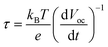 | (3) |
where
τ is the potential dependent photoelectron lifetime,
kB is Boltzmann's constant,
T is the temperature,
e is the charge of a single electron, and
Voc is the open-circuit voltage at time
t. The calculated photoelectron lifetime is shown in
Fig. 4 as a function of
Voc. Clearly, the photoelectron lifetime increases with decreasing
Voc. The nanopore/
nanotube samples (
i.e, S-80-80, S-60-80, S-60-100) showed relatively long electron lifetime, contributing to their high PEC performances.
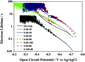 |
| | Fig. 4 Electron lifetime measurements determined from the decay of open circuit potential in dark. | |
EIS is a powerful tool for studying the interfacial properties between electrodes and solutions. The EIS measurements were carried out covering the frequency range of 105–0.1 Hz using an amplitude of 10 mV at the open circuit potential of the system. Fig. 5a presents Nyquist plots for different hierarchical TiO2 NTs photoanodes under illumination. Semicircles in the Nyquist plots convey information on charge transfer process as the diameters of the semicircles are equal to charge transfer resistance of a sample. As depicted in Fig. 5a, the semicircular diameters for the nanopore/nanotube samples are much smaller than others, and S-60-80 shows the smallest arch diameter among all samples, indicating that the nanopore/nanotube samples possess smaller charge transfer resistance and thus better electron mobility. The capacitance measurement on the electrode/electrolyte was conducted at 5 kHz to determine carrier density (ND) of the TiO2 NTs based electrodes following the equation below:31
| | 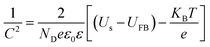 | (4) |
where
C is the space charge capacitance in the semiconductor;
ND is the electron carrier density;
e is the elemental charge value;
ε0 is the permittivity of a vacuum;
ε is the relative permittivity of the semiconductor;
Us is the applied potential;
T is the temperature; and
kB is the Boltzmann constant.
Fig. 5b presents the Mott–Schottky (
MS) plot as
1/
C2vs. potential. The slopes of the linear parts of the curves in the MS plot are positive, indicating n-type semiconductors. The carrier density
ND was determined from
Fig. 5b using the following equation:
31| | 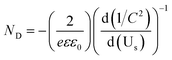 | (5) |
Using
e = 1.6 × 10
19,
ε0 = 8.86 × 10
−12 F m
−1, and
ε = 48 for anatase TiO
2,
32 the carrier densities were calculated and summarized in
Table 1. Among all of the samples, S-60-80 showed the highest carrier density of 8.48 × 10
19 cm
−3. An increase in the
ND value improves the charge transport in semiconductors and it can also shift the Fermi level of the semiconductors toward its conduction band, which further facilitates the charge separation at the semiconductor/electrolyte interface. The enhanced charge separation and charge transport are favorable to PEC performance enhancement.
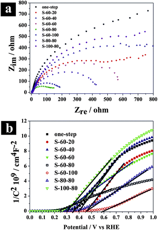 |
| | Fig. 5 (a) Electrochemical impedance spectra of Nyquist plots (Zrevs. Zim), and (b) Mott–Schottky plot at a fixed frequency of 5 kHz on hierarchical TiO2 NTs photoanodes. | |
Conclusion
In summary, the two-step anodization is an effective strategy for the preparation of hierarchical TiO2 NTs. By tuning the voltages used in the anodization processes, morphology, optical absorption and crystallinity can be altered, which allow us to optimize the PEC water splitting performance on these TiO2 NTs photoelectrodes. The optimal photocurrent density and photoconversion efficiency in our system are 1.59 mA cm−2 and 0.84% under illumination of AM 1.5G (100 mW cm−2), the highest values ever reported for single component TiO2 materials. This result points out the possibility of further improving performance in not only PEC systems, but also in solar cells and other photocatalytic fields and thus contributes to high energy conversion devices.
Notes and references
- N. S. Lewis, Science, 2007, 315, 798–801 CrossRef CAS.
- M. G. Walter, E. L. Warren, J. R. McKone, S. W. Boettcher, Q. Mi, E. A. Santori and N. S. Lewis, Chem. Rev., 2010, 110, 6446–6473 CrossRef CAS.
- N. K. Allam, C. W. Yen, R. D. Near and M. A. Ei-Sayed, Energy Environ. Sci., 2011, 4, 2909–2914 CAS.
- P. Roy, C. Das, K. Lee, R. Hahn, T. Ruff, M. Moll and P. Schmuki, J. Am. Chem. Soc., 2011, 133, 5629–5631 CrossRef CAS.
- X. Yang, A. Wolcott, G. Wang, A. Sobo, R. C. Fitzmorris, F. Qian, J. Z. Zhang and Y. Li, Nano Lett., 2009, 9, 2331–2336 CrossRef CAS.
- A. Wolcott, W. A. Smith, T. R. Kuykendall, Y. Zhao and J. Z. Zhang, Adv. Funct. Mater., 2009, 19, 1849–1856 CrossRef CAS.
- K. Sivula, R. Zboril, F. L. Formal, R. Robert, A. Weidenkaff, J. Tucek, J. Frydrych and M. Grätzel, J. Am. Chem. Soc., 2010, 132, 7436–7444 CrossRef CAS.
- D. K. Zhong, M. Cornuz, K. Sivula, M. Grätzel and D. R. Gamelin, Energy Environ. Sci., 2011, 4, 1759–1764 CAS.
- V. Cristino, S. Caramori, R. Argazzi, L. Meda, G. L. Marra and C. A. Bignozzi, Langmuir, 2011, 27, 7276–7284 CAS.
- A. Paracchino, V. Laporte, K. Sivula, M. Grätzel and E. Thimsen, Nat. Mater., 2011, 10, 456–461 CrossRef CAS.
- M. Liu, N. de Leon Snapp and H. Park, Chem. Sci., 2011, 2, 80–87 RSC.
- H. Tang, K. Prasad, R. Sanjjines, P. E. Schmid and F. Levy, J. Appl. Phys., 1994, 75, 2042–2047 CrossRef CAS.
- M. Takahashi, K. Tsukigi, T. Uchino and T. Yoko, Thin Solid Films, 2001, 388, 231–236 CrossRef CAS.
- X. Chen, S. Shen, L. Guo and S. S. Mao, Chem. Rev., 2010, 110, 6503–6570 CrossRef CAS.
- A. Wolcott, W. A. Smith, T. R. Kuykendall, Y. Zhao and J. Z. Zhang, Small, 2009, 5, 104–111 CrossRef CAS.
- X. Feng, K. Shankar, O. K. Varghese, M. Paulose, T. J. Latempa and C. A. Grimes, Nano Lett., 2008, 8, 3781–3786 CrossRef CAS.
- H. E. Prakasam, K. Shankar, M. Paulose, O. K. Varghese and C. A. Grimes, J. Phys. Chem. C, 2007, 111, 7235–7241 CAS.
- P. Roy, S. Berger and P. Schmuki, Angew. Chem., Int. Ed., 2011, 50, 2904–2939 CrossRef CAS.
- S. Li, G. Zhang, D. Guo, L. Yu and W. Zhang, J. Phys. Chem. C, 2009, 113, 12759–12765 CAS.
- D. Wang, B. Yu, C. Wang, F. Zhou and W. Liu, Adv. Mater., 2009, 21, 1964–1967 CrossRef CAS.
- M. Ye, X. Xin, C. Lin and Z. Lin, Nano Lett., 2011, 11, 3214–3220 CrossRef CAS.
- Z. H. Zhang, M. F. Hossain and T. Takahashi, Int. J. Hydrogen Energy, 2010, 35, 8528–8535 CrossRef CAS.
- F. Wang, Y. Liu, W. Dong and Z. Kang, J. Phys. Chem. C, 2011, 115, 14635–14640 CAS.
- J. Yan and F. Zhou, J. Mater. Chem., 2011, 21, 9406–9418 RSC.
- J. Park, S. Bauer, K. von der Mark and P. Schmuki, Nano Lett., 2007, 7, 1686–1691 CrossRef CAS.
- J. M. Macak, H. Tsuchiya and P. Schmuki, Angew. Chem., Int. Ed., 2005, 44, 2100–2102 CrossRef CAS.
- G. Wang, H. Wang, Y. Ling, Y. Tang, X. Yang, R. C. Fitzmorris, C. Wang, J. Z. Zhang and Y. Li, Nano Lett., 2011, 11, 3026–3033 CrossRef CAS.
-
B. D. Cullity, Elements of X-ray diffraction. 2nd ed. Reading, MA: Addison-Welsley; 1978. pp. 283 Search PubMed.
- N. K. Allam and C. A. Grimes, Langmuir, 2009, 25, 7234–7240 CrossRef CAS.
- B. H. Meekins and P. V. Kamat, ACS Nano, 2009, 3, 3437–3446 CrossRef CAS.
- G. Wang, Q. Wang, W. Lu and J. Li, J. Phys. Chem. B, 2006, 110, 22029–22034 CrossRef CAS.
- P. K. Ghosh and M. E. Azimi, IEEE Trans. Dielectr. Electr. Insul., 1994, 1, 975–981 CrossRef.
Footnote |
| † Electronic Supplementary Information (ESI) available: Extra SEM images, crystallize sizes data and open circuit potential vs. time profile. See DOI: 10.1039/c2ee03461a |
|
| This journal is © The Royal Society of Chemistry 2012 |
Click here to see how this site uses Cookies. View our privacy policy here.  Open Access Article
 This Open Access Article is licensed under a Creative Commons Attribution-Non Commercial 3.0 Unported Licence