Recent advances in solution-processed interfacial materials for efficient and stable polymer solar cells
Hin-Lap
Yip
a and
Alex K.-Y.
Jen
*ab
aDepartment of Materials Science and Engineering, University of Washington, Seattle, Washington 98195, USA. E-mail: ajen@u.washington.edu; Fax: +1 206 543 3100; Tel: +1 206 543 2626
bPhotovoltaic Materials, Department of Material Chemistry, Korea University, Korea
First published on 1st February 2012
Abstract
This article provides an overview on the recent development of solution processed organic, inorganic, and hybrid interfacial materials for bulk-heterojunction polymer solar cells. The introduction of proper interfacial materials to optimize the electronic and electrical properties between the interfaces of the light-harvesting active layer and the charge-collecting electrode has become an important criterion to improve the performance of polymer solar cells. The electronic processes at these interfaces play a critical role in determining the efficiency for photon-to-electricity conversion. An ideal interface requires the formation of Ohmic contact with minimum resistance and high charge selectivity to prevent charge carriers from reaching the opposite electrodes. For long-term stability of polymer solar cells, interfaces with matched surface energy are required to prevent interfacial dewetting and delamination. Several classes of interfacial materials including inorganic metal oxides, crosslinkable charge-transporting materials, conjugated polymer electrolytes, self-assembled functional molecules, and graphene-based materials are highlighted and the integration of these interfacial materials with new low bandgap polymers and fullerene derivatives as active materials in different device architectures is also discussed.
 Hin-Lap Yip | Hin-Lap Yip received his BS and MS degrees in Materials Science from Chinese University of Hong Kong in 2001 and 2003, respectively. He received his PhD degree in Materials Science and Engineering from University of Washington in 2008 under the supervision of Prof. Alex Jen. Currently he is a research scientist and thrust leader of the OPV team in Prof. Alex Jen's research group. His research focuses on the use of an integrated approach combining materials, interface, device, and process engineering to improve the OPV technology. He has co-authored over 40 papers and 5 patents in the area of OPV. |
 Alex K.-Y. Jen | Alex Jen is currently the Boeing-Johnson Chair Professor and Chair of the Materials Science and Engineering Department at the University of Washington. He also serves as the Director of the Institute of Advanced Materials for Energy. He has co-authored >500 publications and 50 patents and inventions in the area of organic functional materials and devices. For his pioneering contributions in organic photonics and electronics, he was selected as a Fellow by several professional societies such as AAAS, SPIE, OSA, ACS-PMSE, and ACS. He was also elected as a member of the Washington State Academy of Sciences. |
Broader contextOrganic photovoltaics (OPVs) represent a transformative solar technology with great potential for extremely high-throughput manufacturing at very low cost, and are made from non-toxic, earth-abundant materials with low energy inputs. They can be served as lightweight, flexible, conformal, and low-cost power sources for various applications. Despite the potential of OPVs for large-scale solar deployment, their performance must be improved before they can be viable for commercial applications. Current best OPVs exhibit power conversion efficiencies (PCE) of 8–9% in small size champion cells. Theoretical models suggest that the efficiency could be improved to >10% for single cells and >15% for tandem cells. To achieve these performance goals, advances in the design of new light-harvesting materials and the development of more efficient device processing and stable device structures are required. In addition, interface engineering also plays a critical role in determining the performance of OPV devices. The development of new interfacial materials with desired charge selectivity and compatibility for all-solution-processed multilayer devices, and proper integration of the interfacial layer with new active materials are important to further improve the efficiency and stability of OPVs. In this article, the design criteria and the functions of interfacial layers for OPVs are discussed. |
1. Introduction
Organic photovoltaics (OPVs) have attracted extensive research and development due to their potential as a low cost renewable energy source.1–4Polymer-based OPVs that can be processed from solution are of particular interest and represent a transformative solar technology that can be manufactured by high-throughput roll-to-roll processes, and are made from non-toxic, earth-abundant materials with low energy input.5 Over the past few years, enormous progress has been achieved on improving the performance of OPVs with power conversion efficiencies (PCE) of 8–9% and lifetimes over 6 years (estimated from accelerated testing) demonstrated in small area devices.6–8 Meanwhile, a roll-to-roll industrial manufacturing process has been demonstrated to fabricate OPV modules with efficiencies in the range of 2–3%.9 Though the performance of these OPV modules is relatively low compared to their inorganic counterparts, they have found initial application as battery chargers for portable electronics due to their mechanical flexibility and light-weight. Integration of OPV into functional devices such as OPV-enhanced lighting systems has also been demonstrated and tested for off-grid lighting applications in remote areas.10 However, for widespread deployment of OPV as large-area, roof-top applications for residential and commercial buildings, higher module efficiencies (7–10%) and lifetimes (7–10 years) are required.11To achieve these performance goals, advances in the design of new light-harvesting materials,12–14 and the development of more efficient device processing15–17 and stable device structures18,19 are required. In addition, interface engineering also plays a critical role in determining the performance of OPV devices.20–25 The development of new interfacial materials with desired charge selectivity and compatibility for all-solution-processed multilayer devices, and proper integration of the interfacial layer with new active materials are important to further improve the efficiency and stability of OPVs. In this article, the design criteria and the functions of interfacial layers for OPVs are discussed. Several classes of interfacial materials including metal oxides, crosslinkable charge-transporting materials, conjugated semiconductor electrolytes, self-assembled functional molecules and graphene-based interface materials are highlighted and the integration of these interfacial materials with new low bandgap polymer and fullerene derivatives as active materials in different device architectures is summarized. The fundamental understanding of the surface and interface science, and the device physics associated with the interfaces of OPVs are equally important and in-depth discussions on these areas can be found in several review articles.26–31
2. Functions of interfacial layers
The best OPVs reported to date are composed of a layer of polymer donor and fullerene acceptor bulk-heterojunction (BHJ) film sandwiched between a transparent electrode, such as indium tin oxide (ITO), and a metal electrode. Under illumination, photo-generated excitons will dissociate at the donor–acceptor interface, driven by the difference in energy levels between the two semiconductors. The separated charges will then drift under the inherent electric field created by the work-function difference between the asymmetric electrodes and ultimately will be collected by the corresponding electrodes. The PCE is defined by the product of three parameters including short-circuit current density (Jsc), open-circuit voltage (Voc), and fill factor (FF).J sc is directly related to the efficiencies of light absorption, exciton generation and dissociation, charge transport and charge collection at the electrodes. Voc is related to the difference between the highest occupied molecular orbital (HOMO) of the donor and the lowest unoccupied molecular orbital (LUMO) of the acceptor in the BHJ. More specifically, it is determined by the difference between the quasi-Fermi levels of holes (EF,h) and electrons (EF,e) under illumination provided that barrierless contacts to the electrodes are formed (Fig. 1).28,32 FF is governed by both the parasitic series resistance (Rs) and shunt resistance (Rp) of the solar cell.27,31Rs is determined by the bulk conductivity of the electrodes, active and interfacial layers, and the contact resistance between them. Rp is determined by the quality of the thin films and their interfaces. Small Rp originates from the loss of charge carriers through leakage paths including pinholes in the films and the recombination and trapping of the carriers during their transit through the cell that can lead to decreased device performance. The nature of electrical contact between the BHJ layer and the electrodes can significantly affect all three device-related parameters and modification of those interfaces by inserting appropriate interfacial layers can significantly alter the contact properties to improve the PCE of OPVs.
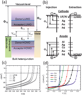 | ||
| Fig. 1 (a) Energy level diagram of an OPV device composed of a transparent electrode/active layer/metal electrode structure. (b) Schematic energy diagram of an interface between an organic layer and different metal cathode (upper) and anode (bottom). The extraction current for electrons and holes is independent of the work-function of the cathode and anode, respectively. (c) J–V curves of the ITO/PEDOT:PSS/OC1C10-PPV:PCBM/cathode conventional OPV under illumination, with different metal electrodes. Reprinted with permission from ref. 32. Copyright 2003, The American Institute of Physics. (d) J–V curves of ITO/ZnO/P3HT:PCBM/anode inverted OPV under illumination, with different metal electrodes. | ||
The interfacial layer can serve multiple functions that include:
1. Tuning the energy level alignment at the electrode/active layer interface
In BHJ OPVs, the maximum achievable Voc is dependent on the difference between the quasi-Fermi levels of the photoinduced holes, EF,h, in the donor and the photoinduced electrons, EF,e, in the acceptor (depicted as Voc1 in Fig. 1). This result can only be obtained if Ohmic contacts are formed with both cathode and anode. When a Schottky contact is formed on either side, or both sides, of the BHJ/electrode interface, the Voc will be reduced. The magnitude of this reduction is determined by the static internal electric field across the device, which is a result of the difference between the work functions of the electrodes according to the metal–insulator–metal (MIM) model (Voc2 in Fig. 1a).32Understanding of the interfacial electronic structure and energy level alignment at the electrode/BHJ contact is important for designing better contacts to improve charge extraction for OPVs. However, the nature of electronic contact formation between the electrode and active layer can be very complicated since a wide variety of interfacial effects including charge transfer, dipole formation, formation of interface states, etc. can occur depending on the type and strength of interactions between the two materials and the order of contact formation such as organic-to-metal or metal-to-organic.33
One of the most widely considered interfacial effects for OPV is the Fermi-level pinning of electrodes to the negative integer charge-transfer state (EICT−) of the acceptor (equivalent to EF,e) and positive integer charge-transfer state (EICT+) of the donor (equivalent to EF,h) due to the corresponding electron and hole transfer from the electrode to the organic layer.34–36 This integer charge-transfer (ICT) model is particularly suitable to describe interfaces formed by solution processing of materials under ambient conditions in which there is negligible hybridization between the π-electronic molecular orbitals and the substrate wave functions.
The ICT model has been used to describe three scenarios at the substrate/organic interface: (1) when the substrate work function is lower than the EICT− of the organic semiconductor, electrons will transfer from the substrate to the organic semiconductor and the Fermi level will eventually be pinned to the EICT−; (2) when the substrate work function is in between EICT− and EICT+, no Fermi level pinning occurs; and (3) when the substrate work function is higher than the EICT+ of the organic semiconductor, holes will transfer from the substrate to the organic semiconductor and the Fermi level will eventually be pinned to the EICT+. These results have been verified experimentally on a wide range of conjugated polymers and fullerenes.34,37
However, there are several parameters that may affect the use of the ICT model to predict the interface behavior between the electrodes and BHJ film since the composition of polymer and fullerene can vary across the film depending on the processing conditions and surface energy of the substrate.38–40 In addition, undesired chemical reactions or metal diffusion into the polymer film can occur when energetic metal atoms are deposited through thermal evaporation to form the top electrode.41 Brabec et al. studied the effect of different metal cathodes in the ITO/PEDOT:PSS/MDMO-PPV:PCBM/metal devices and observed a very small variation of Voc from 0.81 V to 0.65 V when the work function of the cathode varied from 2.9 eV (Ca) to 5.1 eV (Au).42 This can be explained by Fermi level pinning of the electrode to the reduction potential of fullerene, which facilitates Ohmic contact at the cathode interface. As a result, a scaling factor (S) of 0.1 was observed, where S is defined as the quotient of the difference in Voc and the difference of the work function of the electrodes.
Mihailetchi et al. performed a similar study based on a device configuration of ITO/PEDOT:PSS/OC1C10-PPV:PCBM/metal with various metal cathodes including LiF/Al, Ag, Au, and Pd (Fig. 1b). The results showed that only LiF/Al formed Ohmic contact with the BHJ while other metals form non-Ohmic contact with a scaling factor S closed to 1 (Fig. 1c).32,43 Another interesting finding in this study is that the energy barrier (ΦB) presented in the non-Ohmic metal/organic junctions does not contribute to additional contact resistance for the OPV devices. This can be explained by the difference between the charge injection and the charge extraction processes, as depicted schematically in Fig. 1b. For OPVs, the extraction of electrons from the LUMO of the acceptor to a higher work function cathode is an energy barrier-free process, which does not inhibit electrons from leaving the active layer.
The same mechanism can also be applied for the extraction of holes from the HOMO of the donor to a lower work function anode. The effect of metal anodes on the Voc of OPVs has also been investigated in ITO/ZnO/P3HT:PCBM/metal based inverted devices. A series of metals with increasing work functions from Al (4.3 eV) to Pd (5.3 eV) were studied and only high work function Pd was found to form Ohmic contact for hole extraction. The Voc of the inverted cells decreased with the decrease of the work functions of the anode with a scaling factor S of 0.6 (Fig. 1d).44 By inserting a conductive PEDOT:PSS film between the BHJ and the metal anode, it enabled the achievement of maximum Voc independent of the choice of metals. This suggested that the high work function PEDOT:PSS layer (5.1 eV) can facilitate Fermi-level pinning to the EICT+ of the BHJ film to facilitate Ohmic contact formation.
Based on the aforementioned findings, it can be concluded that the Voc can reach the upper limit defined by the difference between the quasi-Fermi levels of hole and electron in the BHJ when Ohmic contacts are formed at both electrodes. Ohmic contact at the cathode can be formed by choosing electrodes with work functions lower than the ICT− energy of the acceptor in the BHJ. Electron transfer from the electrode to the acceptor will result in Fermi level pinning at the ICT−. Ohmic contact at the anode can be formed by choosing electrodes with work functions higher than the ICT+ energy of the donor in the BHJ, hole transfer from the electrode to the donor will result in the Fermi level alignment and pinning at the ICT+. For non-Ohmic contacts, Voc is governed by the difference between the effective work function of the two electrodes. The scaling factor can vary depending on the BHJ systems and device architectures. The application of interfacial materials can be an effective way to tune the work functions of electrodes to achieve Ohmic contact.
2. Defining polarity of electrodes and improving charge selectivity
Since interfacial layers can be used to tune the work functions of both bottom and top electrodes, inclusion of appropriate interfacial layers can alter charge extraction efficiency and selectivity by matching the Fermi level to either the EF,h of the donor or the EF,e of the acceptor in the BHJ for hole or electron collection, respectively. Therefore, OPVs can be fabricated based on two types of device structures including the conventional structure and the inverted structure in which the electrode polarity is reversed (Fig. 2). These two basic architectures can be further developed to construct the tandem structure or semitransparent OPVs.45–48 In the conventional approach, a p-doped conducting polymer, PEDOT:PSS, is commonly used to modify ITO to improve hole extraction and low work function metals such as LiF/Al and Ca/Al are often used as the top cathode to ensure effective electron extraction.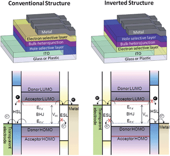 | ||
| Fig. 2 Device architecture of conventional OPV (upper left) and inverted OPV (upper right). Schematic view of the energy level alignment in a conventional OPV (bottom left) and an inverted OPV (bottom right) with interfacial layers providing Ohmic contacts and charge selectivity at both electrodes. | ||
As the low work function metal is vulnerable to oxidation under ambient conditions, electrode degradation is a major concern for this type of device.49 By inserting an ESL between the BHJ and metal cathode can avoid the use of LiF or Ca to improve the interfacial stability.18 In some cases, even stable metals such as Cu and Ag can be used as cathode when appropriate interfacial materials are applied.50,51 To further enhance device stability, one can implement an inverted device structure with an ESL (such as TiO2 or ZnO) inserted between ITO and the active layer to selectively collect electrons, while a more air-stable, high work function metal can be used as top anode for hole collection.52–54 Inverted OPVs not only have superior ambient stability but also possess better compatibility to all-solution roll-to-roll processing since the metal anode can be deposited from colloidal solution (e.g.Ag nanoparticles).9,55
In addition to modification of the electrode work function to facilitate Ohmic contact, interfacial layers can also be used to improve charge selectivity at the electrode/active layer interface. Since in a homogeneously mixed BHJ layer both donor and acceptor are in contact with the electrodes, therefore undesired charge recombination and exciton quenching can occur at the electrodes to decrease the device performance. By introducing interfacial layers with proper charge selectivity, it can minimize undesired interfacial charge recombination and lead to improved rectification of the J–V response and FF of the device.
The idealized band structures for the charge selective layers in both conventional and inverted devices are shown in Fig. 2. Both ESL and hole selective layer (HSL) should have appropriate energy alignment with the acceptor and donor for barrierless extraction of electrons and holes to the cathode and anode. While their corresponding HOMO (valence band) and LUMO (conduction band) should provide energy barriers to block the flow of holes and electrons to the cathode and anode, respectively. Interfacial layers with bandgaps larger than those of the donor and acceptor may also help confine excitons in the active layer to increase the chance for exciton dissociation.56 However, in some cases, the interfacial layer can also be designed to provide an additional exciton dissociation interface.57
Electrical conductivity is another important factor that needs to be considered when designing interfacial layers since materials with high conductivity can minimize the resistance loss of the device. High conductivity can also reduce the voltage drop across the interfacial layers and maximize the internal field across the active film, which can improve field-dependent exciton dissociation.58 Conductivity becomes even more important when the device is biased near Voc, at which point the internal field is diminished, and a sufficiently large electrical field across the BHJ is needed to suppress the recombination loss. Doping of semiconductors is an efficient approach not only to improve the electrical conductivity of the interfacial layer but also to tune their Fermi energy for achieving Ohmic contact at the electrode/active layer interface.59
For small molecule based OPV devices prepared viavacuum deposition, controlled doping of interfacial layers by co-deposition of dopants and small molecules is generally used to create p–i–n junctions for high-performance devices.59 In polymer solar cells, PEDOT:PSS is extensively applied as a hole-transporting layer to improve hole collection at the anode. However, the electron-blocking capability of PEDOT:PSS is not optimal and the recent reports on using highly conductive PEDOT:PSS as an electron-collecting electrode further suggest that PEDOT:PSS does not possess adequate electron-blocking capability for OPV.60–62 The development of new solution-processed p-doped and n-doped interfacial layers remains to be a challenging area for OPVs since it requires careful design of semiconductors and dopants that are stable under ambient conditions, in addition to being soluble and robust enough to support multilayer film processing from solution. Recent advances in the development of new materials that can simultaneously fulfil those requirements will be discussed in the next section.
3. Controlling surface properties to alter the morphology of the active layer
The microstructure of the BHJ layer significantly affects the light harvesting, exciton dissociation, charge transport and charge collection in OPVs. The capability to generate a morphology that can simultaneously fulfil these aspects is critical for improving device performance.63,64 An ideal morphology is composed of phase-separated domains of donor and acceptor with sizes that are comparable to the exciton diffusion length (∼10 nm) in order to minimize exciton recombination. These domains should form an interpenetrating network that provides efficient charge transport pathways in each material towards the corresponding electrodes. The vertical phase separation in the BHJ layer also plays a crucial role in the charge transport and collection processes.Enhanced charge selectivity at the corresponding electrodes can be achieved by ensuring donor (acceptor) enrichment at the anode (cathode) interfaces. The desirable vertical composition gradient for OPV devices in the conventional and inverted structures is shown in Fig. 3. In addition to the nanoscale phase separation and vertical composition, the orientation of the backbone of the polymer donor with respect to the substrate can also affect the light-harvesting and charge-transporting properties in the BHJ film. Polymer backbones preferentially oriented parallel to the substrate surface can result in improved light absorption and charge transport in the vertical direction of the device.65–67
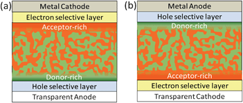 | ||
| Fig. 3 Schematic illustration of the desired vertical phase separation of polymer:fullerene blend in (a) conventional OPV and (b) inverted OPV. | ||
Development of effective methods to control the morphology of the BHJ layer is another important task to improve device performance. However, it remains a challenging one since the film formation process is a complex interplay involving interactions between processing solvent, donor/acceptor pairs, and substrate surfaces.63 Typical approaches used to optimize the morphology include selecting the appropriate solvent, tuning the rate of drying, and fine-tuning thermal and vapor annealing conditions.15,68 Controlling the drying kinetics and molecular interactions in the BHJ film through processing with additives has recently been established as an efficient approach to improve the morphology and performance of OPVs.69 In fact, most of the high efficiency devices recently reported have all been prepared using this approach.65,70–72 Tuning the surface energy and surface chemistry via self-assembled monolayer-based interfacial layers provides another powerful means to manipulate the vertical and lateral phase separation of the BHJ film.73 They can also potentially be used to control the orientation of the polymer backbone and generate patterned nanostructures.74,75
Based on the consideration of simple interfacial free energy, during the film drying process, components with lower surface energy (γ) in the blend will selectively segregate towards the low γ air interface (free surface) while components with γ matched with that of the substrate will enrich at the buried interface to minimize the free energy. The effect of substrate surface energy on the vertical composition of BHJ has been investigated using the P3HT:PCBM system. In general, P3HT, which has a low γ of 26.9 mN m−2, is enriched at the top of the BHJ film independent of the substrate γ. Slight enrichment of PCBM (γ = 37.8 mN m−2) was observed at the buried interface on PEDOT:PSS (γ = 45 mN m−2).39,76 Such a vertical composition is not desired for conventional OPV devices but more favorable for inverted structure devices in which the PCBM-rich buried interface and P3HT-rich top surface can enhance electron and hole collection at the bottom cathode and top anode, respectively.77 Recently, a new device fabrication method (ESSENTIAL) which is compatible with roll-to-roll processing has been introduced to improve the OPV performance through efficient control of the BHJ film morphology by replacing the air interface with an elastomer stamp during the film drying process, which further demonstrates the importance of controlling surface energy in achieving optimized OPV performance.78
4. Introducing optical spacer and plasmonic effects to modulate light absorption in the active layer
The development of solution processable light management schemes to enhance light harvesting in the active layer represents another important strategy to improve the performance of OPVs. The inferior charge-transporting properties of organic semiconductors compared to their inorganic counterparts limit the light harvesting layer thickness to be ∼100 nm in order to minimize the charge recombination loss. However, to absorb all the incident light, it usually requires a film to have a greater thickness. This dilemma can be potentially resolved by using light-trapping strategies which allow the light harvesting layer thickness to be reduced while still keeping the effective optical thickness constant.Many light-trapping strategies have been explored to improve optically thin OPV devices including folded device architectures,79 aperiodic dielectric stacks,80 diffraction gratings,81,82 optical spacers,83,84 and plasmonic nanostructures.85 Interfacial engineering is particularly important in realizing the latter two light-trapping schemes. Most OPV devices are composed of an active layer sandwiched between a transparent electrode and a reflective metal electrode. The incident light enters the OPV cell through the transparent electrode and is reflected back into the active layer at the metal electrode forming a standing wave within the device. The ability to control the interference effects to maximize the optical field strength within the thin film is particularly important for improving light absorption. The introduction of proper interfacial layers as optical spacers between the active layer and electrodes can effectively modulate the optical field in the active layer to improve OPV performance.86
Fig. 4a shows an example of how the electrical field distribution in the active layer can be tailored to improve light harvesting in the P3HT:PCBM model system by tuning the refractive index and thickness of the optical spacers, electrode reflectivity, and device structure.86 The simulated electrical field intensity in different device configurations correlates strongly with experimental device results. The optimization of optical spacer effects can play an even more critical role in improving the performance of tandem OPVs in which a higher degree of optical management is required to simultaneously improve the absorption in different subcells.87
 | ||
| Fig. 4 (a) Schematic drawing of OPV devices composed of different interfacial layers and their corresponding simulated electric field intensity within the P3HT:PCBM BHJ layers for light of incident wavelength λ = 550 nm. Reprinted with permission from ref. 86. Copyright 2011, Wiley-VCH Verlag GmbH & Co. KGaA. (b) Schematic representation of light trapping through forward scattering as a result of metal NP induced LSPR (left). The optical path length increased because light was trapped through multiple and high-angle scattering. Schematic representation of the local enhancement of the electromagnetic field (right). The plasmonic field decays exponentially with respect to the distance from the surface of the metal NPs. Reprinted with permission from ref. 88. Copyright 2011, American Chemical Society. (c) Schematic drawing of plasmon-enhanced charge carrier generation in the P3HT:PCBM film using Ag nanoprisms. Reprinted with permission from ref. 90. Copyright 2010, American Chemical Society. (d) Schematic of a plasmonic polymer tandem solar cell in which the interconnection layer is doped with Au NPs. Reprinted with permission from ref. 89. Copyright 2011, American Chemical Society. | ||
Light trapping based on the surface plasmon resonance effect of metallic nanostructures is another promising strategy to improve light harvesting for OPVs.88–90 The placement of the metal nanostructures in different positions of the device is important to manipulate different optical enhancement effects including light scattering and localized surface plasmon resonance (LSPR). Embedding metal nanoparticles directly in the active layer can potentially utilize light scattering effect to improve the optical path within the light absorbing layer,91 while near field enhancement of electromagnetic fields through LSPR can result in absorption enhancement in the active material surrounding the nanoparticles.88
However, the presence of ill-defined metal–organic interfaces can enhance nonradiative decay processes and increase carrier recombination, which may not result in a net positive effect on PCE. By embedding the metal nanoparticles in the interfacial layers, it can potentially mitigate charge quenching at the nanoparticle/active layer interface while improving light harvesting in the active layer (Fig. 4b). The results from recent reports also have provided experimental evidence that LSPR generated from the metal nanoparticles embedded in the doped interfacial layer can not only enhance the light absorption of the active layer but also reduce the recombination of geminate excitons close to the contact between the BHJ and the interfacial layers.88 Shape-controlled metallic nanoparticles with tunable LSPR peaks and high ratios of scattering to absorption loss may further enhance the plasmonic effect for OPV. Indeed, silver nanoprisms have already been shown to increase the photocarrier generation yield in optically thin OPV films by up to 300% over a range of wavelengths (Fig. 4c).90 The plasmonic effects could also be applied to improve polymer tandem cells in which metal nanoparticles were doped into the interconnecting layer, resulting in light absorption enhancement in both top and bottom cells and a 20% improvement in PCE (Fig. 4d).89
5. Improving interfacial stability between the active layer and electrodes
Other than PCE, stability is another important aspect that needs to be improved to make OPV a competitive solar technology. Compared to their inorganic counterparts, organic semiconductors are intrinsically more susceptible to chemical degradation, especially under illumination in the presence of oxygen and water. Several degradation pathways of OPV have been identified including chemical degradation of active materials, interfacial materials, electrodes and their interfaces, and physical degradation of BHJ layer morphology.49 Although device encapsulation can slow down the degradation processes by impeding oxygen and water diffusion into the device, synergistic development of more stable materials, interfaces, and device structures that are fully compatible with ambient roll-to-roll processing is equally important.Therefore, the development of intrinsically stable interfacial layers that can serve as protective layers to prevent undesired physical and chemical reactions between electrodes and the active layer is critical to further improve the stability of OPV. For the modification of anode, PEDOT:PSS is the most commonly used interfacial material, showing good electrical properties and processability that enables the fabrication of high-efficiency conventional and inverted OPV devices. However, several reports suggest that the acidic nature of PEDOT:PSS can negatively affect interfacial stability because it can react with ITO to cause the diffusion of In ions into both PEDOT:PSS and the active layer, which will degrade both materials.92,93 In addition, the diffusion of silver into PEDOT:PSS to form electrical shorting paths was also reported for the inverted cells (Fig. 5a and b).94 Moreover, the ease of moisture and oxygen absorption in PEDOT:PSS can alter its microstructure and reduce its conductivity.95 These results suggested that although PEDOT:PSS has been used in early OPV modules, it is unlikely to be the ultimate interfacial layer for stable OPV technology. Inorganic interfacial materials that can function as a diffusion barrier to H2O and O2 can provide good protection for the active layer. This property has been demonstrated in densely packed TiOx systems showing both good electron selectivity and improved device stability (Fig. 5c).18
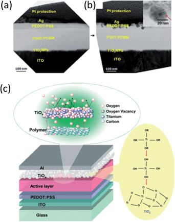 | ||
| Fig. 5 Cross-sectional TEM images showing the interface between the silver and PEDOT:PSS layer of an inverted OPV cell conserved in the dark for three months after fabrication (a) and after additionally exposure to ambient environment for eleven weeks (b). The inset in (b) is an enlarged image of silver particles formed at the interface. Reprinted with permission from ref. 94. Copyright 2010, Cambridge University Press. (c) The device architecture with the TiOx layer, as ITO/PEDOT:PSS/active layer/TiOx/Al. The TiOx layer functions as a scavenging layer to block the permeation of oxygen and moisture into the polymer active layer. The brief flow chart shows the preparation steps of the TiOx. Reprinted with permission from ref. 18. Copyright 2007, Wiley-VCH Verlag GmbH & Co. KGaA. | ||
Finally, interfacial materials that can form conformal contacts with improved adhesion between the active layer and electrodes are critical to prevent interfacial dewetting and delamination. This is especially true for flexible polymer solar cells that may need to be operated under constant mechanical stress. Interfacial delamination is known to be one of the major failure modes in other thin film-based solar cells, however there is a limited amount of information regarding this issue as it pertains to polymer solar cells. Recent reports on engineering the adhesive properties of interfacial materials and their use as electronic “glue” at the active layer/electrode interface highlight a new approach to potentially improve the long-term stability of OPVs, however, more detailed studies are required.96–98
3. Overview of interfacial materials
Significant progress has been made in the past few years in the area of interfacial materials for OPVs and some of these developments have been extensively reviewed in other reports.20,23,25 Therefore, here we only focus on discussing some of the most recent advancements on the design and application of interfacial materials in different device architectures.In general, efficient interfacial materials for OPV should fulfil several requirements with regard to their electronic, electrical, optical, chemical and mechanical properties. They should (i) promote Ohmic contact formation between electrodes and the active layer; (ii) have appropriate energy levels to improve charge selectivity for corresponding electrodes; (iii) have large bandgap to confine excitons in the active layer; (iv) possess sufficient conductivity to reduce resistive losses; (v) have low absorption in the Vis-NIR wavelengths to minimize optical losses; (vi) have chemical and physical stability to prevent undesirable reactions at the active layer/electrode interface; (vii) have the ability to be processed from solution and at low temperatures; (viii) be mechanically robust to support multilayer solution processing; (ix) have good film forming properties and (x) be producible at low cost.
It is challenging to identify a single material system that can simultaneously fulfil all these requirements but several classes of materials and their hybrids had been explored including conducting polymers, metal oxides, crosslinkable materials, conjugated polymer electrolytes, self-assembled functional molecules and graphene-based materials. The design concepts and the interfacial properties of these materials in both conventional and inverted OPV structures will be discussed. Also highlighted is the integration of these interfacial materials with high performance low bandgap polymers and fullerene derivatives as active materials to produce stable and efficient OPV devices. The chemical structures of some of the conjugated polymer donors and fullerene acceptors that will be discussed are shown in Fig. 6. The energy levels of these active materials and the commonly used HSLs and ESLs are presented in Fig. 7.
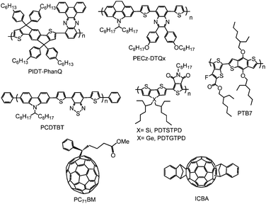 | ||
| Fig. 6 Molecular structures of selected conjugated polymer donors and fullerene acceptors used as active materials in BHJs. | ||
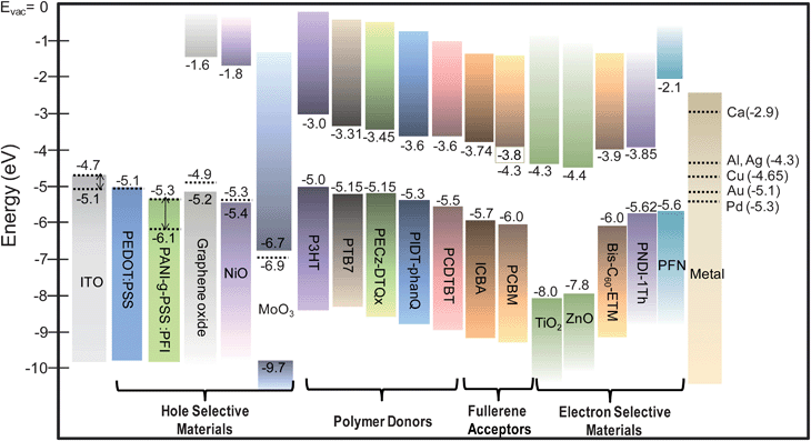 | ||
| Fig. 7 Schematic view of the energy gaps and energy levels of some of the components of recent OPVs including transparent electrodes, hole selective materials, polymer donors, fullerene acceptors, electron selective materials and metal electrodes. The dotted lines correspond to the work functions of the materials. | ||
3.1. Interfacial materials for conventional structure OPVs
The device characteristics of conventional structure OPVs employing different interfacial layers are summarized in Table 1. A conducting polymer, PEDOT:PSS, is the most commonly used solution-processable hole-transporting layer for anode modification in conventional solar cells. PEDOT:PSS is obtained directly in the p-doped state (PEDOT+) by oxidative polymerization of ethylenedioxythiophene in an aqueous emulsion in the presence of PSSH, forming a PEDOT+:PSS−polyelectrolyte complex. One of the advantages of PEDOT:PSS is that a wide range of electrical conductivities from 10−6 to 103 S cm−1 can be achieved by changing the compositional ratio between PEDOT+ and PSS− and by processing with additives to modify the microstructure of PEDOT:PSS films. This provides great flexibility in tuning the electrical property at the active layer/electrode interface. PEDOT:PSS also has good optical transparency over the Vis-NIR range which minimizes absorption loss. Another advantage of PEDOT:PSS is its work function (∼−5.1 eV), which matches well with the EF,h of a wide range of polymer donors to form good Ohmic contact at the anode/BHJ layer interface. Some of the best reported OPV efficiencies are those using PEDOT:PSS as the hole-transporting layer.70,71| Anode configuration | Active layer | Cathode configuration | V oc/V | J sc/mA cm−2 | FF | PCE (%) | Ref. |
|---|---|---|---|---|---|---|---|
| ITO/PEDOT:PSS | P3HT:PC61BM | Ca/Al | 0.61 | 10.6 | 0.67 | 4.4 | 15 |
| ITO/PANI-g-PSS | P3HT:PC61BM | Al | 0.59 | 10.9 | 0.62 | 4.0 | 101 |
| ITO/SPDPA | P3HT:PC61BM | Ca/Al | 0.60 | 10.3 | 0.68 | 4.2 | 103 |
| ITO/TFB:PABTSi2 | P3HT:PC61BM | LiF/Al | 0.54 | 9.3 | 0.63 | 3.1 | 108 |
| ITO/TPA-PFCB/PEDOT:PSS | P3HT:PC61BM | Ca/Al | 0.61 | 9.4 | 0.67 | 3.9 | 109 |
| ITO/BT-BTPA/p-IDT-BTPA | PIDT-phanQ:PC71BM | Ca/Al | 0.85 | 9.5 | 0.66 | 5.5 | 110 |
| ITO/NiO (sputtered) | P3HT:PC61BM | LiF/Al | 0.64 | 11.3 | 0.69 | 5.2 | 60 |
| ITO/NiOx (sol–gel) | PCDTBT:PC71BM | Ca/Al | 0.88 | 11.5 | 0.65 | 6.7 | 113 |
| ITO/VOx (sol–gel) | P3HT:PC61BM | Al/Ag | 0.53 | 9.6 | 0.59 | 3.0 | 114 |
| ITO/MoO3 (vac) | PCDTBT:PC71BM | TiOx (sol–gel)/Al | 0.89 | 10.9 | 0.67 | 6.5 | 121 |
| ITO/MoO3 (NPs) | P3HT:PC61BM | Al | 0.57 | 7.7 | 0.67 | 2.9 | 125 |
| ITO/graphene oxide | P3HT:PC61BM | Al | 0.57 | 11.4 | 0.54 | 3.5 | 127 |
| ITO/PEDOT:PSS | P3HT:PC61BM | TiOx (sol–gel)Al | 0.61 | 11.1 | 0.66 | 5.0 | 84 |
| ITO/PEDOT:PSS | PCDTBT:PC71BM | TiOx (sol–gel)/Al | 0.88 | 10.6 | 0.66 | 6.1 | 133 |
| ITO/PEDOT:PSS | P3HT:PC61BM | TiO2:Cs NPs/Al | 0.58 | 10.8 | 0.67 | 4.2 | 135 |
| ITO/PEDOT:PSS | P3HT:PC61BM | ZnO NPs/SAM/Al (Ag, Au) | 0.65 | 11.1 | 0.63 | 4.6 | 137 |
| ITO/PEDOT:PSS | P3HT:PC61BM | ZnO NPs-PEG/Al (Ag, Au) | 0.60 | 10.7 | 0.69 | 4.4 | 139 |
| ITO/PEDOT:PSS | P3HT:PC61BM | P(VDF-TrFE)/Al | 0.59 | 12.8 | 0.60 | 4.5 | 140 |
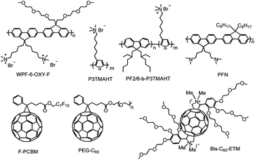
| ITO/PEDOT:PSS | P3HT:PC61BM | WPF-6-oxy-F/Al (Cu, Ag, Au) | 0.64 | 10.1 | 0.60 | 3.9 | 51 |
| ITO/PEDOT:PSS | PCDTBT:PC71BM | PF2/6-b-P3TMAHT/Al | 0.89 | 10.6 | 0.67 | 6.5 | 147 |
| ITO/PEDOT:PSS | PECz-DTQx-PC71BM | PFN/Al | 0.81 | 11.4 | 0.66 | 6.1 | 148 |
| ITO/PEDOT:PSS | PTB7:PC71BM | PFN/Ca/Al | 0.76 | 15.8 | 0.70 | 8.4 | 149 |
| ITO/PEDOT:PSS | P3HT:PC61BM | PEG-C60/Al (Cu, Au) | 0.66 | 10.5 | 0.65 | 4.4 | 154 |
| ITO/PEDOT:PSS | PIDT-phanQ:PC71BM | C60-surfactant/Ag (Al, Cu) | 0.88 | 11.5 | 0.61 | 6.2 | 50 |
However, for a polymer donor with a very deep HOMO level (−5.64 eV), a further increase in PEDOT:PSS work function is required to create Ohmic contact for maximizing the Voc.99 Other concerns regarding PEDOT:PSS are its electrical and structural inhomogenities, which originate from the insulating PSS layer, and can limit the charge collection.100 In addition, the acidic and hygroscopic nature of PSS can induce chemical instability between the active layer and electrodes.93 The electron-blocking capability of PEDOT:PSS towards common OPV acceptors is also questionable since several reports have suggested that PEDOT:PSS can even be used as an electron-collecting electrode.61
These deficiencies have sparked the vigorous material development trying to find replacement for PEDOT:PSS. The chemical structures of some of the newly developed HSLs are shown in Fig. 8. Several other conducting polymers have been explored including a self-doped, grafted copolymer (PSSA-g-PANI), the conductivity and acidity of which can be easily tuned by adjusting the molar ratio between PSSA and PANI.101 OPV devices based on optimized PSSA-g-PANI film showed better thermal stability and PCE than those obtained from the PEDOT:PSS-based control device. PSSA-g-PANI can also be processed with perfluorinated ionomer (PFI) to tune its work function. A wide range of work functions from 5.28 eV to 6.09 eV can be obtained upon increasing the PFI blending ratio.102 OPV devices based on the PFI-doped PSSA-g-PANI showed a more than 30-fold increase in lifetime compared to the PEDOT:PSS-based device. The authors attributed the improved stability to the efficient metal ion (In/Sn) blocking property of the PFI layer. Another self-doped conducting polymer, sulfonated poly(diphenylamine) (SPDPA), also showed promise as a PEDOT:PSS replacement.103 The introduction of dopants directly onto the backbone of the conjugated polymer can potentially eliminate the insulating PSS− induced electrical inhomogeneity. However, the acidic and hygroscopic nature of these conducting polymers may lead to similar degradation problems as found in PEDOT:PSS.
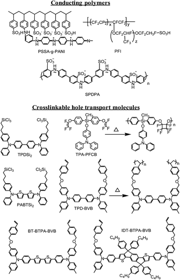 | ||
| Fig. 8 Molecular structures of some hole selective materials including conducting polymers and crosslinkable hole transport materials. | ||
Crosslinkable charge-transporting materials are another class of interfacial materials that have already shown their promise in controlling the charge injection and extraction properties of organic light-emitting diodes104 and photodetectors,105 respectively. The chemical structures of several promising crosslinkable materials are shown in Fig. 8. The HOMO/LUMO levels, bandgaps and the hole mobility of these materials can be tuned by rational molecular design while the crosslinkers are introduced on the active components as pendant groups. As a result, these materials can be thermally or photochemically crosslinked to form robust charge-transporting films with improved solvent resistance for subsequent processing of the BHJ layer.
Hains and Marks have demonstrated that a robust hole-selective layer can be formed through silane-based crosslinking reactions.106–108 The hole mobility of the HSL can be improved by doping with a conjugated polymer (TFB). The HOMO levels of the HSLs (−5.3 eV for TPDSi2 and −4.9 eV for PABTSi2) can be further tuned to match those of the donors in the BHJ film to create a barrier free interface for efficient hole extraction.108 Good charge selectivity of the crosslinkable HTL can also be realized in bilayer structure devices where a thin HSL (TPA-PFCB) is initially polymerized at 225 °C, then inserted between ITO and PEDOT:PSS to afford both enhanced Voc and Jsc in OPV cells through efficient blocking of electrons.109 This approach also improves the interfacial stability by preventing PEDOT:PSS from reacting with ITO.
A novel hybrid HSL inspired by the bilayer approach and consisting of a p-doped and a neutral layer has been developed to combine the high conductivity of a p-doped, crosslinkable HTM with the good electron-blocking ability of a neutral crosslinkable HTM to achieve better contact and hole selectivity at the anode.110 This was realized by using a carefully designed crosslinkable HTM system (BT-BTPA-BVB and IDT-BTPA-BVB) with the core structures consisting of different extended aromatic backbones bookended by two triarylamine groups. This design provides good tunability of the energy levels, charge transport, and optical properties of the HTMs. By introducing a styrene-based crosslinker, it allows the HTMs to be crosslinked at a relatively low temperature between 150 and 180 °C. After the formation of a robust layer, a controlled doping using nitrosonium hexafluoroantimonate (NOSbF6) as the p-dopant improved the conductivity and optical transparency of the HTMs.
The hole-selecting property of these materials was tested in devices composed of new low bandgap polymer donors (e.g. PIDT-PhanQ) in the BHJ layer. The device with the bilayer structure composed of a p-doped IDT-BTPA-BVB layer on top of a neutral BT-BTPA-BVB layer showed significantly enhanced Voc, Jsc, and FF compared to the devices with only a single layer of doped crosslinked HTM. This molecular engineering approach of developing new materials in order to control the charge-selecting and transporting properties can be very important for future development of OPVs.
p-Type transition metal oxides such as vanadium oxides (V2O5)111 and nickel oxides (NiO)60 have also been used as another class of hole-selecting materials for OPVs. These large bandgap metal oxides possess good optical transparency in the visible and near infrared regions, which allows photons to reach the active layer. In addition, the conduction band of these p-type semiconducting oxides is sufficiently higher than the LUMO of both organic donor and acceptor materials, which effectively blocks electron leakage through the anode. The high work functions of p-type metal oxides (NiO ≈ 5.3 and V2O5 ≈ 5.3 to 5.4 eV) also can promote good Ohmic contact at the BHJ/anode interface with minimal contact resistance. As a result, good diode characteristics and fill factors of ∼70% could be achieved in OPVs using optimized p-type NiO layers which is a significant enhancement over PEDOT:PSS devices.60
However, most of the p-type metal oxide films in earlier studies were prepared through vacuum deposition processes, which are incompatible with the high throughput printing processes. Therefore, further development of efficient metal oxides through the low temperature, solution-based processes is needed. Recently, good quality NiOx films prepared by a sol–gel method with thermal annealing at moderate temperatures (300 °C), followed by O2 plasma treatment, were tested as HSL in the PCDTBT:PC71BM BHJ devices.112,113 The results were very promising with high PCE (6.7%) and better stability than those PEDOT:PSS-based devices due to improved hole selectivity and contact. Another report regarding a HSL based on a sol–gel derived VOx film annealed at lower temperature (110 °C) also showed quite encouraging results with its device performance comparable to that of PEDOT:PSS-based devices but with better stability.114 However, the optical absorption of VOx in the visible range (400–500 nm) may limit its application as an efficient HSL.
Molybdenum oxides (MoO3) and tungsten oxides (WO3) are other transition metal oxides that have also been extensively investigated for anode modification in OPVs.111,115 Recent studies on the electronic structures of MoO3 and WO3 revealed that both oxides are n-type with deep-lying electronic states.116,117 For example, the measured electron affinity, work function and ionization potentials for vacuum-deposited MoO3 are −6.7 eV, −6.86 eV and −9.68 eV, respectively, making it unlikely to behave as a HSL.117 Indeed, the improved electrical properties at the metal oxide/organic interface were due to the interfacial p-doping effect. Since the conduction band of MoO3 is significantly deeper than the HOMOs of common organic semiconductors, p-doping through interfacial electron transfer from the organic semiconductor to MoO3 is thermodynamically favorable. This interfacial p-doping effect was reported for various polymers,118 small molecules,119 and even fullerenes.120 The interfacial stability of OPVs based on the evaporated MoO3 film has been studied in different BHJ systems (P3HT:PC61BM and PCDTBT:PC71BM) and the results showed that greatly enhanced lifetime could be achieved compared to the PEDOT:PSS-based devices.121,122 The recent demonstration of MoO3 interfacial layers in OPV devices using either sol–gel processes123,124 or nanoparticle solutions125,126 further showed the promise of using metal oxides for anode modification.
Graphene oxide (GO) is another very interesting material that has shown promise as an efficient HSL for OPVs.127 GO is an oxidized derivative of graphene, which can be prepared by chemical oxidation of naturally abundant graphite in large quantities and at low cost. Its solution processability and unique electrical and optical properties endow it as a promising nanomaterial for various applications. The bandgap of GO was reported to be 3.6 eV, while its HOMO and LUMO were measured to be −5.2 eV and −1.6 eV, respectively. The work function of GO was measured by scanning Kelvin probe microscopy, showing values between −4.9 and −5.1 eV.128 These energy levels suggest that GO can transport holes and block electrons and excitons, making it a potential good hole selective material for OPV. Li et al. first explored the use of GO as HSL in P3HT:PCBM-based OPV and demonstrated that devices based on a thin layer of GO nanosheets (2 nm) could have comparable performance to that of PEDOT:PSS-based devices. However, the devices with thicker GO films showed lower performance due to the insulating nature of GO.127 To gain a better understanding of the interfacial electronic processes at the ITO/GO/BHJ interfaces, the authors have performed transient open-circuit voltage delay (TOCVD) measurements to study the dependence of charge recombination kinetics of the BHJ film on different substrates. The results showed that the charge recombination rate in the ITO/GO/BHJ sample is lower than that in the ITO/BHJ and ITO/PEDOT:PSS/BHJ samples, suggesting that GO is more effective in suppressing leakage current and separating carriers via efficient hole-transporting to ITO and blocking of electrons.
To further improve the anode contact, a hybrid bilayer structure based on GO and sol–gel processed NiOx was developed.129 OPVs with different combinations of HSLs including GO, NiOx, NiOx/GO and GO/NiOx were compared and the best device performance was found in the GO/NiOx structure, showing major improvement of FF. The authors attributed this improvement to better energy alignment between ITO and the P3HT:PCBM BHJ. In addition, the reduced surface roughness of the GO/NiOx film further reduced the series resistance across the device. These encouraging findings have opened the way for developing new interfacial materials for OPV.
Interface engineering for cathode is also very important for improving the performance of OPVs. In conventional OPVs, vacuum-deposited thin films of low work function metals such as Al, LiF/Al or Ca/Al are often used for electron collection. However, low work function metals are vulnerable to oxidation and tend to form an unstable cathode contact. To improve the cathode contact in convention cells, several other vacuum-deposited materials such as BCP,130 PCBM,131 and C60:LiF132 have been introduced between the BHJ layer and the Al cathode to achieve improved interfacial stability and electron collection. However, the development of solution processable ESLs is important for printable OPVs. The optimized ESLs should support the use of more stable and printable metals (such as colloidal Ag) as cathode for roll-to-roll manufacturing of OPV.
n-Type metal oxides like TiO2 and ZnO are the most widely studied ESL for OPVs. These oxides are transparent in the Vis-NIR spectrum and their conduction band energies are well matched with the electron transport energy of fullerene acceptors and their deep valence band energies can also effectively block holes. Using low temperature sol–gel processing, amorphous TiOx films can be directly deposited on a BHJ layer to fabricate OPV devices.84 The TiOx films not only showed good electron selectivity but also functioned as an optical spacer and a good water and oxygen barrier, leading to significantly improved device efficiency and stability. The optical spacer effect of TiOx has also been investigated in different BHJ systems. A PCE of 6.1% has been reported when the TiOx interfacial layer was applied to a PCDTBT:PC71BM BHJ solar cell.133
Furthermore, by replacing the PEDOT:PSS layer with MoO3, the PCE of a PCDTBT:PC71BM device increased to 6.5% and the stability of the device also improved significantly. This is attributed to the use of metal oxides at both electrode/active layer interfaces.121TiO2 films prepared from solution processed crystalline nanoparticles (NPs) can also be used as an efficient ESL for OPVs.134 By doping TiO2 NP with Cs, it can further decrease the work function for more efficient electron extraction. As a result, the P3HT/PCBM based solar cells showed enhancements in PCE compared to those using a pure TiO2 ESL.135
ZnO is another efficient n-type metal oxide used for cathode modification in OPVs. The electronic structure of ZnO is very similar to that of TiO2, making it a good electron selective material. One advantage of solution processed ZnO NP films is a high electron mobility (2.5 cm2Vs−1),136 which can minimize Ohmic loss in the device. The electrical and electronic properties of ZnO can also be easily tuned by modifying the ZnO surface with a self-assembled molecular layer.137,138 This provides a versatile way to engineer the contact between the ZnO buffer layer and different metal cathodes. By using SAMs that can form favorable dipoles and covalent bonding between ZnO and metal, devices showed significant improvement in efficiency and it also enabled high work function metals such as Ag and Au to be used as cathode.137 These findings have paved the way for using solution processable metal electrodes for low-cost polymer solar cells since a thin film Ag electrode can be easily printed from its precursor solution. Hybridization of ZnO NPs with poly(ethylene glycol) can also be used to engineer the work function, morphology, refractive index and charge transporting properties of the ESL, which provides an efficient way to improve OPV performance.139
Organic-based interfacial materials that can be processed through orthogonal solvents of the BHJ layer are another class of promising electron selective materials for OPVs and the chemical structures of the materials are highlighted in Fig. 9. Recently, an ultrathin (1 nm) layer of ferroelectric polymer, P(VDF-TrFE), has been inserted between different BHJs and Al cathode to show significantly improved device characteristics.140 The authors suggested that the device improvement was the result of forming large, permanent, internal electric field by the ferroelectric polymer, which facilitated more efficient exciton dissociation in the BHJ. However, another report suggested that the improved efficiency in ferroelectric polymer modified OPVs may be simply due to better Ohmic contact at the cathode.141 Therefore, a better understanding of the role of the ferroelectric effect in these devices is required to effectively apply this type of polymer to OPVs.
 | ||
| Fig. 9 Molecular structures of some electron selective materials used in conventional OPVs including conjugated polymer electrolytes and fullerene-based interfacial materials. | ||
Conjugated polymers and polymer electrolytes that can be processed from alcoholic/water solvents represent another class of promising electron selective materials that has attracted significant research attention in the past two years.51,142–150 This class of polymers had already shown promising results in improving electron injection in OLEDs.151 For OPV applications, polythiophene and polyfluorene based conjugated polymers with side chains containing polar moieties, such as amines, amine salts, phosphates, and alkoxy groups, are the most commonly investigated systems. Oh et al. have demonstrated that an ESL based on a water soluble polyfluorene derivative (WPF-oxy-F) can effectively reduce the work functions of different metals including Al, Ag, Cu and Au, resulting in Ohmic contact between the P3HT:PC61BM BHJ and cathode.51 As a result, the Voc and PCE of the OPV devices were nearly independent of the choice of metal used for cathode. Seo et al. have studied the effect of cationic polythiophene (P3TMAHT) and its polyfluorene block copolymer derivative (PF2/6-b-P3TMAHT) on PCDTBT:PC71BM based devices. In both cases, the devices showed significantly improved PCE from 5% to over 6.3%.147 The authors attributed the improved efficiency to the local dipole arrangement in the thin cationic polymers, which modified the contact with Al electrode. This, in turn, led to reduced series resistance and increased shunt resistance compared to the control device. It is interesting to note that the hole-transporting property of the polythiophene backbone did not seem to affect the electron selectivity at the cathode contact. A better understanding of the interfacial electronic structures at these interfaces will be an interesting topic for further investigation.
The effect of another water/alcohol soluble polyfluorene derivative, PFN, which contains side chains terminated with neutral alkylamines has also been studied with BHJs composed of different polymer donors.146 It was found that the improvements of PCE rely heavily on the chemical structures of the polymer donors. Though the effect of PFN on P3HT and PPV-based OPVs was minimal, significant improvement of the PCE in a group of N-heterocycle-containing polymer donors was effectively demonstrated.144 For example, OPVs based on PECz-DTQx:PC71BM showed PCE increases from 4.0% to 6.1% when Al was used as cathode,148 while for the PCDTBT:PC71BM BHJ, the best device employed the PFN ESL in combination with a Ca/Al cathode, showing a PCE of 6.8%.149 The authors suggested that the N–N interactions between the PFN and the N-heterocycle-containing polymers might play a role in determining the cathode contact properties.
In a recent study, the authors further expanded the application of the PFN ESL to another high performance low bandgap polymer, PTB7, and demonstrated a record OPV device performance with a PCE of 8.4%.149 The authors suggested that the improved device performance could have multiple origins including enhanced built-in potential across the device, improved charge transport, reduced space charge buildup, and minimized recombination losses due to increases in built-in field and charge carrier mobility.
Fullerene-based interfacial materials present another obvious option for ESL in BHJ OPVs since their energy levels, electron transport, and chemical compatibility to the BHJ fit the requirements of a good ESL. However, there are only limited reports of fullerene-based ESL, which is probably due to the challenge in synthesizing proper fullerene materials with adequate solubility that can be used for solution processing. PCBM derivatives with fluorinated alkyl (F-PCBM)152 and polymer(ethylene glycol) (PEG-C60)153,154 are two interesting fullerene derivatives that have been explored as ESL. In both cases, small amounts of the fullerene derivatives were added to the P3HT:PCBM solution. During the film drying process, a thin layer of the fullerene derivative was found to segregate on the surface of the BHJ film, forming a self-organized interfacial layer. The OPV devices were then completed by evaporation of an Al cathode. In both cases, the fullerene surfactants were found to interact with the Al electrode, forming an appropriate interfacial dipole that promoted better Ohmic contact and improved the device performance. Although the simplicity of self-organized ESLs is very attractive, it may not be generally applicable to different BHJ systems since the film drying kinetics may vary in different polymer:fullerene blends.
Therefore, fullerene derivatives that can be directly processed on top of different BHJ layers might represent a better option for preparing fullerene ESLs. This has been recently realized in a new fullerene derivative (bis-C60-ETM) in which side chains composed of an amine salt and an alkoxy dendron were introduced to improve its solubility in alcohols.50 The bis-C60-ETM could be directly spin-coated on top of the active layer to form a smooth ESL. To evaluate the general applicability of the fullerene ESL, devices based on different BHJs were tested and, in all cases, the devices with bis-C60-ETM showed significantly improved Voc, Jsc, FF, and PCE. The effect of different metal cathodes (Al, Ag, and Cu) on the OPV efficiency and stability was further investigated based on the PIDT-phanQ:PC71BM BHJ system. The best PCE (6.2%) was found when Ag was used as the cathode. Work function studies suggested that the bis-C60-ETM film efficiently reduced the effective work functions of all three metals, which facilitated Ohmic contact at the BHJ/cathode interface to achieve a maximized Voc independent of the choice of metal. However, devices with Cu and Ag cathodes showed much better ambient stability than the one with Al. These findings can be very important for developing efficient, stable, and roll-to-roll processable polymer solar cells.
3.2. Interfacial materials for inverted structure OPVs
Since their initial application in 2006, inverted OPVs have attracted growing attention due to their improved stability and compatibility with roll-to-roll processes.155–157 For inverted OPVs, the device polarity is reversed compared to that based on the conventional structure. The performance of the inverted OPV is critically dependent on the choice of the interfacial layers and their contact properties with the BHJ layer and the corresponding electrodes. The device characteristics of the representative inverted OPVs containing different interfacial layers and BHJ layers are summarized in Table 2.| Cathode configuration | Active layer | Anode configuration | V oc/V | J sc/mA cm−2 | FF | PCE (%) | Ref. |
|---|---|---|---|---|---|---|---|
| ITO/Cs2CO3 | P3HT:PC61BM | V2O5/Al | 0.59 | 11.1 | 0.63 | 4.2 | 159 |
| ITO/TiOx (sol–gel) | P3HT:PC61BM | PEODT:PSS/Au | 0.56 | 9.0 | 0.62 | 3.1 | 54 |
| ITO/TiOx/FPQ-Br | P3HT:PC61BM | MoO3/Au | 0.58 | 8.9 | 0.70 | 3.6 | 162 |
| ITO/WPF-6-oxy-F | P3HT:PC61BM | PEDOT:PSS/Ag | 0.66 | 8.8 | 0.59 | 3.4 | 163 |
| ITO/ZnO (sol–gel) | PDTGTPD:PC71BM | MoO3/Ag | 0.85 | 12.6 | 0.68 | 7.3 | 72 |
| ITO/ZnO (sol–gel) | PCDTBT:PC71BM | MoO3/Ag | 0.88 | 10.4 | 0.69 | 6.3 | 165 |
| ITO/ZnO (sol–gel) | aPTPTBT:PC71BM | VOx (sol–gel)/Ag | 0.82 | 11.6 | 0.53 | 5.0 | 166 |
| ITO/ZnO NPs | P3HT:PC61BM | PEDOT:PSS/Ag | 0.62 | 10.7 | 0.54 | 3.6 | 19 |
| ITO/ZnO NPs/C60-SAM | P3HT:PC61BM | PEDOT:PSS/Ag | 0.63 | 12.0 | 0.61 | 4.5 | 168 |
| ITO/ZnO (sol–gel)/C-PCBSD | P3HT:PC61BM | PEDOT:PSS/Ag | 0.60 | 12.8 | 0.58 | 4.4 | 171 |
| ITO/ZnO (sol–gel)/C-PCBSD | P3HT:ICBA | PEDOT:PSS/Ag | 0.84 | 12.4 | 0.60 | 6.2 | 172 |
| ITO/n-doped P-PCBM-S | P3HT:PC61BM | PEDOT:PSS/Ag | 0.63 | 9.1 | 0.44 | 2.5 | 174 |
| ITO/n-doped PNDI-1Th | P3HT:PC61BM | PEDOT:PSS/Ag | 0.59 | 10.0 | 0.58 | 3.4 | 175 |
| ITO/SPMA | P3HT:PC61BM | V2O5/Al | 0.60 | 10.5 | 0.57 | 3.6 | 178 |
| ITO/(P3PHT/PEDOT:PSS)n | P3HT:PC61BM | V2O5/Al | 0.54 | 7.1 | 0.46 | 1.9 | 179 |
| ITO/TiO2 | P3HT:PCBM | SPDPA/Au/Ag | 0.58 | 10.5 | 0.64 | 3.9 | 182 |
| ITO/ZnO (sol–gel) | P3HT:PC61BM | TPD-BVB/Au | 0.60 | 7.9 | 0.62 | 3.0 | 183 |
| ITO/ZnO NPs/C60-SAM | P3HT:PC61BM | GO/Ag (Au, Al) | 0.62 | 10.3 | 0.62 | 3.9 | 185 |
| ITO/ZnO NPs | PIDT-phanQ:PC71BM | GO/Ag | 0.86 | 10.9 | 0.62 | 5.9 | 187 |
Alkali metal salts can be used as an interfacial modifier to tune the work function of ITO for electron collection.158 By using spin-cast Cs2CO3 for ITO modification and V2O5 as the HSL underneath the Al top electrode, the PCE of inverted P3HT:PCBM BHJ OPVs could reach as high as 4.2%.159 It was found that upon annealing at 150 °C, Cs2CO3 will decompose into doped caesium oxide (Cs2O). This significantly improved electron collection by reducing the work function of ITO from 4.7 eV to 3.06 eV.96 However, the insulating property of Cs2O may limit its broader application for OPVs.
Similar to the cases in conventional cells, TiO2 and ZnO are the most widely studied electron selective materials for inverted OPVs. These n-type metal oxide semiconductor films can effectively modify the ITO electrode to facilitate efficient electron collection. Since the charge-transporting properties of the metal oxide films are strongly dependent on their microstructures and crystallinities, significant research efforts have been focused on the development of new thin film deposition methods to improve these properties.160,161 The low temperature sol–gel process has been used to deposit titanium sub-oxide (TiOx) on ITO to fabricate inverted OPVs based on P3HT:PCBM BHJ, showing a PCE of ∼3.1%.54
Modification of the TiOx film with a polyfluorene-based polymer electrolyte (FPQ-Br) further improved the Jsc and FF of the device, leading to a PCE of 3.6%.162 The polymer electrolyte introduced an interfacial dipole that lowered the energy barrier between the ITO and BHJ, resulting in reduced interfacial contact resistance. Some conjugated polymer electrolytes, such as the WPF-6-oxy-F, can even be directly applied as ESL on ITO.163 The water-soluble WPF-6-oxy-F can reduce the work function of ITO from 4.66 eV to 4.22 eV, making it more suitable for electron extraction from the BHJ layer. Inverted P3HT:PCBM devices based on a thin layer of WPF-6-oxy-F ESL showed a PCE of 3.4%.
Although the use of the low temperature process for fabricating TiOx films is more favorable for practical applications, the low electron mobility (1 × 10⁻⁴ cm2Vs−1) of the resulting film may detract from their utility in high-performance devices.84 Thermal annealing at temperatures over 400 °C can convert the amorphous film into the crystalline TiO2 film and thereby improve its charge-transporting properties.57 Nevertheless, the high temperature process is not compatible with plastic substrate used for roll-to-roll processing. To circumvent this problem, a new method combining electrochemical deposition followed by high pressure crystallization was used to produce the crystalline TiO2 film on ITO at a relatively low temperature (150 °C) to fabricate inverted OPVs.161
ZnO has a similar band structure to TiO2 but higher electron mobility, which is advantageous for reducing the electrical resistance in OPVs. White et al. have demonstrated one of the earliest inverted P3HT:PCBM BHJ solar cells based on a sol–gel derived ZnO film on ITO as the ESL and an Ag anode as the top electrode.53 The crystallinity of the ZnO films could be increased by thermal annealing at 300 °C to improve their electrical properties. By inserting a thermally evaporated HSL, such as V2O5 or MoO3 between the BHJ layer and metal anode, it promotes better Ohmic contact at the anode, leading to further improved ZnO-based inverted OPVs.164 Such a device platform has shown good compatibility with different BHJ layers. Recently, very high efficiency inverted OPVs were demonstrated based on PDTSTPD:PC71BM and PDTGTPD:PC71BM BHJ layers with PCEs of 6.6% and 7.3%, respectively.72
The effect of different thermal annealing temperatures of sol–gel derived ZnO films on the performance of inverted PCDTBT:PC71BM OPV has also been studied with relatively low temperatures (130 °C, 150 °C and 200 °C) applied to anneal the ZnO films.165 As expected, the electron mobility of the films increased with the increase of annealing temperature. The best inverted OPV was obtained from a ZnO film annealed at 200 °C with a PCE of 6.3%, while a decreased PCE was found for devices based on lower temperature annealed ZnO films due to an increased series resistance. In addition to the development of solution processed n-type metal oxides as ESL, the development of solution processed p-type metal oxide as HSL for inverted cells is equally important. Chen et al. have demonstrated that a VOx HSL could be prepared by spin-coating the sol–gel solution on the BHJ layer followed by low temperature annealing at 100 °C.166 Inverted P3HT:PC61BM and PTPBT:PC71BM devices showed enhanced performance as a result of increased Jsc. The encapsulated inverted devices also showed very good thermal stability with no performance loss after annealing at 65 °C for 1000 h. These results are very encouraging since the low temperature process is more compatible with flexible plastic substrates.
The modification of metal oxide films with functional SAMs can efficiently alter the interfacial properties between the ESL and BHJ. Bulliard et al. reported that the morphology of the BHJ film could be optimized by virtue of a ZnO surface with tailored surface energy leading to an improved PCE in inverted cells.73 This can be achieved by changing the surface compositions of the two different SAMs with either polar –NH2 or non-polar –CH3 end groups, resulting in a wide range of surface energies from 40 mN m−1 to 70 mN m−1. Modification of metal oxides with fullerene-based SAMs has also been employed to improve the ESL/BHJ contact. Fullerene-based SAMs utilizing different anchor groups were designed to tune their self-assembling properties on ZnO.167 It was found that good quality fullerene-SAM (C60-SAM) could be obtained by the simple spin-coating process if they have proper anchor groups. The C60-SAM (Fig. 10) serves multiple purposes, including enhancement of interfacial exciton-dissociation efficiency, passivation of inorganic-surface trap states, and optimization of the upper organic layer morphology. As a result, a C60-SAM modified P3HT:PCBM inverted cell showed improved PCE from 3.7% to 4.5%.168 This strategy has also been applied to other BHJ layer composed of new low bandgap polymers, which resulted in similar improvement in device efficiency.169
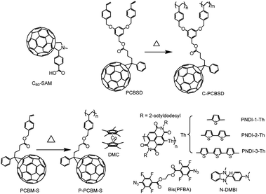 | ||
| Fig. 10 Molecular structures of electron selective materials used in inverted OPV including fullerene self-assembled molecule, crosslinkable fullerene derivatives, crosslinkable n-type polymers and different n-dopants. | ||
The interfacial property between the metal oxide ESL and the BHJ can also be improved by inserting a thin layer of crosslinked fullerenes (C-PCBSD) (Fig. 10).170,171In situ cross-linking of the PCBSD film on ZnO could be achieved by annealing the film at 160 °C for 30 min to generate a robust, adhesive, and solvent-resistant film. It could also planarize the ZnO surface to provide a more uniform contact with the BHJ layer. C-PCBSD offers similar interfacial effects compared to the C60-SAM modified ZnO ESL, showing an improvement of the performance of inverted P3HT:PCBM OPV from 3.5% to 4.4%. The application of a ZnO/C-PCBSD bilayer ESL has been expanded to further improve new BHJ systems based on the indene-C60 bis-adduct (ICBA) acceptor.172 The ICBA has a smaller LUMO energy level compared to PCBM, which can improve the Voc of OPV. As a result, the inverted OPV device incorporating a ZnO/C-PCBSD ESL showed a high PCE of 6.2%, while the control device only showed a PCE of 4.8%.
Compared to their inorganic counterparts, the use of pure n-type organic semiconducting materials as ESL is much less explored in spite of their promise as interfacial materials for OPVs. The ability to tune their electrical and physical properties through molecular design makes them an attractive class of materials. Additionally, organic materials are more suitable for flexible OPVs because of their intrinsic mechanical robustness. However, the major limitation of using organic semiconductors as interfacial materials is their relatively low inherent conductivities, which may result in poor electrical contact with the electrodes. To overcome this limitation, n-doping of organic-based ESL has been applied to improve the contact.173–175 A thermally polymerizable fullerene derivative (PCBM-S) was used as the ESL to provide good solvent resistance necessary to support multilayer processing.174 The electrical properties of the PCBM-S films were systematically tuned by doping with a highly electron-deficient decamethylcobaltocene (DMC), which acts as an efficient solution processed n-dopant. The electrical conductivity of the polymerized PCBM-S film was found to increase with dopant concentration, improving over ∼6 orders of magnitude from 1.7 × 10⁻⁷ S m−1 in the undoped film to 6.0 × 10⁻¹ S m−1 when doped with 10% of DMC. The inverted device performance showed a strong dependence on the conductivity of the ESL. For the undoped ESL, an S-shape J–V feature was observed due to poor electrical contact while devices with an optimized n-doped ESL showed much-improved J–V characteristics and much higher PCE than the undoped device.
n-Doping has also been utilized to develop new ESLs based on crosslinkable n-type conjugated polymers. An in situ n-doping and crosslinking of a series of naphthalene diimide and thiophene copolymers (NPDI-Th) has been used to generate highly conductive ESLs.175 Crosslinking was facilitated by the photo-induced reaction between the singlet nitrene from the bis-PFPA crosslinker and the side chain of the polymer,176 while thermally induced electron transfer from the N-DMBI dopant to the polymer resulted in n-doping.177 The energy levels of the polymers could be modified by systematic tuning of their chemical structures to improve electron selectivity. For example, the LUMO of NPDI-1-Th is −3.85 eV, which matches well with that of PCBM for electron extraction, while the deep HOMO of −5.6 eV can efficiently block holes from most polymer donors. n-Doping of the crosslinked polymer film resulted in significant increased electrical conductivity, as a result, the PCE of inverted P3HT:PCBM OPVs increased from 0.69% to 3.42%. The PCE is even higher than the control device using ZnO as ESL. This promising result opens the way for achieving all-organic OPVs and can be applied to polymeric interfacial materials for solution processing of multilayer solar cell devices.
ESLs based on self-assembly have also been reported. Motiei et al. used a self-propagating molecule-based assembly (SPMA) in which a pyridine functionalized Ru-complex was allowed to coordinate with PbCl2 to construct layer-by-layer molecular stacks as ESL.178 The energy levels of the SPMA ESL could be tailored by the molecular design of the Ru-complex, which had a LUMO of −4.0 eV and a HOMO of −6.1 eV in the reported case. The number of molecular stacks could also be well controlled to tune their interfacial property. Inverted OPV showed a PCE of 3.6% when an optimized thickness of the SPMA ESL of ∼2 nm was used. Further increasing the thickness of the SPMA ESL decreased the device performance due to the low conductivity of the ESL. Electrostatic layer-by-layer self-assembly of a PEDOT:PSS−Na+ and a cationic polythiophene functionalized with pyridine side chains (P3PHT+Br−) has also been employed to prepare multilayers of P3PHT/PEDOT:PSSn as ESL for inverted cells.179 The work function of the ESL was measured to be −4.8 eV, which is lower than that of PEDOT:PSS (−5.1 eV), making it more suitable for electron extraction. As a result, the inverted device based on P3HT:PCBM BHJ showed a PCE of ∼1.9% and Voc of 0.54 V when an optimized ESL of (P3PHT/PEDOT:PSS)5 was used.
Several classes of interfacial materials have been used for anode modification in inverted cells. Thermally evaporated n-type metal oxides such as WO3 and MoO3 are efficient materials that can promote Ohmic contact between the BHJ layer and metal anode due to their ability to p-dope the polymer donor.118,180,181 Besides the widely used PEDOT:PSS, the self-doped conducting polymer SPDPA, with a work function of −5.25 eV, is another promising option for HSL in inverted cells, showing PCEs as high as 3.9% in P3HT:PCBM based devices.182 One of the concerns for using conducting polymers as a HSL is their interfacial stability, which was recently identified as a major degradation pathway for inverted cells. Therefore, the development of new HSL materials must consider how to improve the stability of inverted cells. Crosslinkable hole-transporting materials represent an attractive alternative to PEDOT:PSS in inverted cells. Sun et al. demonstrated that a HSL based on a thermally crosslinked TPD-BVB (Fig. 8) film could improve the electron-blocking property in inverted OPV and the device stability under ambient conditions when compared to devices fabricated with PEDOT:PSS.183 One of the possible reasons for the superior long-term ambient stability is the hydrophobic nature of the C-TPD-BVB, which minimized water absorption-induced device degradation which is commonly found in PEDOT:PSS-based devices.
Anode modification of inverted OPVs using GO as the HSL was also reported.184–186 Due to its good dispersity in polar alcoholic solvents, GO can be directly deposited on BHJ without causing erosion of the active materials. Inverted P3HT:PCBM-based OPV devices modified with a 2–3 nm thick of GO HSL exhibited a remarkable improved PCE compared to devices without any interfacial layer and it is even slightly better than that of PEDOT:PSS-based devices, indicating GO can effectively modify the anode to facilitate efficient hole collection.184 To further elucidate the origin of device improvement in GO-modified inverted OPVs, the interfacial interaction between the BHJ and GO was studied. It was found that protonic acid doping of the conjugated polymer at the BHJ/GO interface occurred due to the high proton density of GO, resulting in a highly conductive interface that facilitated Ohmic contact with the metal anode.185 This finding represents a new strategy for improving the electrical property across the BHJ/metal interface and can be very useful to develop high performance OPVs. A good example was recently demonstrated in inverted OPV based on PIDT-PhanQ:PC71BM BHJ, which showed a PCE of 5.9% when GO was used as the HSL.187
4. Conclusions and Outlook
The current challenges for OPV research are to improve cell and module efficiencies to above 10% in low-cost, lightweight and flexible formats and with lifetime suitable for commercial applications. To achieve these goals, tremendous progress has been made on the design and process of new active materials, development of more stable device structures, and the development of efficient manufacturing processes.Interface engineering plays an equally important role for improving the efficiency and stability of OPVs. In this article, the functions and impact of interfacial layers on the performance of OPVs were discussed. We also reviewed a wide range of materials that have been explored as interfacial layers including conducting polymers, metal oxides, crosslinkable materials, conjugated polymer electrolytes, self-assembled functional molecules and graphene-based materials. All these different classes of materials showed potential but none of them proved to be the perfect choice since each has its own advantages and disadvantages with regard to the electronic, electrical, optical, chemical and mechanical properties. Therefore, the development of new interfacial materials and further understanding and control of the chemical and physical properties at these interfaces are very important to the further improvement of the OPV technology.
In order to better integrate interface engineering into the other rapidly developing areas of OPV research including materials, device, electrode and process engineering, we have identified several key interface-related issues that require further investigation. These areas include:
1. Development of interfacial materials as interconnection layers for tandem solar cells
Tandem OPVs have shown good potential for achieving higher PCE than single-layer OPVs. Since tandem cells are composed of multiple sub-cells, the optimization of interfacial properties becomes even more important. The interfacial layers need to have adequate solvent resistance to facilitate the solution processing of multilayer cells. To ensure appropriate current matching, charge recombination between the sub-cells needs to occur in specially designed p–n junction interconnection layers.2. Development of interfacial materials tailored for non-ITO transparent electrodes
Although ITO is the most commonly used transparent electrode for OPV devices, its high production cost and incompatibility with flexible devices make it unlikely to be the ultimate choice for flexible OPVs. Currently, significant research has been focused on the development of new transparent electrodes such as conducting polymers, carbon nanotubes, graphenes, and metal nanowire networks which all show good potential as ITO replacements. However, there are very few studies dedicated to the understanding of the interfacial properties between the new transparent electrodes and the BHJ-based devices.3. Development of interfacial materials with improved adhesion between electrodes and the active layer
Interfacial materials that can form conformal contacts and improved adhesion between the active layer and electrodes are critical for long-term stability of OPVs. This is particularly important for flexible OPVs that may need to be operated under constant mechanical stress. In addition, the interfaces in OPVs formed between metal oxides, organics, and metals all have very different mechanical properties. Therefore, design of interfacial materials that can improve the mechanical robustness at different interfaces of OPVs is an important research topic.Acknowledgements
This work is supported by the National Science Foundation's NSF-STC program under Grant No. DMR-0120967, the AFOSR (FA9550-09-1-0426), the Office of Naval Research (N00014-11-1-0300), AOARD (FA2386-11-1-4072) and the World Class University (WCU) program through the National Research Foundation of Korea under the Ministry of Education, Science and Technology (R31-10035). A. K.-Y.J. thanks the Boeing-Johnson Foundation for financial support.References
- C. J. Brabec, N. S. Sariciftci and J. C. Hummelen, Adv. Funct. Mater., 2001, 11, 15–26 CrossRef CAS.
- S. Gunes, H. Neugebauer and N. S. Sariciftci, Chem. Rev., 2007, 107, 1324–1338 CrossRef.
- B. C. Thompson and J. M. J. Frechet, Angew. Chem., Int. Ed., 2008, 47, 58–77 CrossRef CAS.
- C. J. Brabec, S. Gowrisanker, J. J. M. Halls, D. Laird, S. J. Jia and S. P. Williams, Adv. Mater., 2010, 22, 3839–3856 CrossRef CAS.
- R. Gaudiana and C. Brabec, Nat. Photonics, 2008, 2, 287–289 CrossRef CAS.
- M. A. Green, K. Emery, Y. Hishikawa, W. Warta and E. D. Dunlop, Prog. Photovoltaics, 2011, 19, 565–572 Search PubMed.
- R. F. Service, Science, 2011, 332, 293 CrossRef CAS.
- C. H. Peters, I. T. Sachs-Quintana, J. P. Kastrop, S. Beaupre, M. Leclerc and M. D. McGehee, Adv. Energy Mater., 2011, 1, 491–494 CrossRef CAS.
- F. C. Krebs, S. A. Gevorgyan and J. Alstrup, J. Mater. Chem., 2009, 19, 5442–5451 RSC.
- F. C. Krebs, T. D. Nielsen, J. Fyenbo, M. Wadstrom and M. S. Pedersen, Energy Environ. Sci., 2010, 3, 512–525 CAS.
- G. Dennler, M. C. Scharber and C. J. Brabec, Adv. Mater., 2009, 21, 1323–1338 CrossRef CAS.
- E. Bundgaard and F. C. Krebs, Sol. Energy Mater. Sol. Cells, 2007, 91, 954–985 CrossRef CAS.
- Y. J. Cheng, S. H. Yang and C. S. Hsu, Chem. Rev., 2009, 109, 5868–5923 CrossRef CAS.
- Y. Liang and L. Yu, Acc. Chem. Res., 2010, 43, 1227–1236 CrossRef CAS.
- G. Li, V. Shrotriya, J. S. Huang, Y. Yao, T. Moriarty, K. Emery and Y. Yang, Nat. Mater., 2005, 4, 864–868 CrossRef CAS.
- J. Peet, M. L. Senatore, A. J. Heeger and G. C. Bazan, Adv. Mater., 2009, 21, 1521–1527 CrossRef CAS.
- F. C. Krebs, Sol. Energy Mater. Sol. Cells, 2009, 93, 394–412 CrossRef CAS.
- K. Lee, J. Y. Kim, S. H. Park, S. H. Kim, S. Cho and A. J. Heeger, Adv. Mater., 2007, 19, 2445–2449 CrossRef CAS.
- S. K. Hau, H.-L. Yip, N. S. Baek, J. Zou, K. O'Malley and A. K. Y. Jen, Appl. Phys. Lett., 2008, 92, 253301 CrossRef.
- H. Ma, H.-L. Yip, F. Huang and A. K. Y. Jen, Adv. Funct. Mater., 2010, 20, 1371–1388 CrossRef CAS.
- L.-M. Chen, Z. Xu, Z. Hong and Y. Yang, J. Mater. Chem., 2010, 20, 2575–2598 RSC.
- E. D. Gomez and Y.-L. Loo, J. Mater. Chem., 2010, 20, 6604–6611 RSC.
- R. Steim, F. R. Kogler and C. J. Brabec, J. Mater. Chem., 2010, 20, 2499–2512 RSC.
- J. H. Park, T.-W. Lee, B.-D. Chin, D. H. Wang and O. O. Park, Macromol. Rapid Commun., 2010, 31, 2095–2108 CrossRef CAS.
- R. Po, C. Carbonera, A. Bernardi and N. Camaioni, Energy Environ. Sci., 2011, 4, 285–310 CAS.
- S. Braun, W. R. Salaneck and M. Fahlman, Adv. Mater., 2009, 21, 1450–1472 CrossRef CAS.
- W. J. Potscavage, Jr, A. Sharma and B. Kippelen, Acc. Chem. Res., 2009, 42, 1758–1767 CrossRef.
- E. L. Ratcliff, B. Zacher and N. R. Armstrong, J. Phys. Chem. Lett., 2011, 2, 1337–1350 CrossRef CAS.
- C. Deibel and V. Dyakonov, Rep. Prog. Phys., 2010, 73, 096401 CrossRef.
- J. Hwang, A. Wan and A. Kahn, Mater. Sci. Eng., R, 2009, 64, 1–31 CrossRef.
- P. W. M. Blom, V. D. Mihailetchi, L. J. A. Koster and D. E. Markov, Adv. Mater., 2007, 19, 1551–1566 CrossRef CAS.
- V. D. Mihailetchi, P. W. M. Blom, J. C. Hummelen and M. T. Rispens, J. Appl. Phys., 2003, 94, 6849–6854 CrossRef CAS.
- H. Ishii, K. Sugiyama, E. Ito and K. Seki, Adv. Mater., 1999, 11, 605–625 CrossRef CAS.
- C. Tengstedt, W. Osikowicz, W. R. Salaneck, I. D. Parker, C. H. Hsu and M. Fahlman, Appl. Phys. Lett., 2006, 88, 053502 CrossRef.
- I. Lange, J. C. Blakesley, J. Frisch, A. Vollmer, N. Koch and D. Neher, Phys. Rev. Lett., 2011, 106, 416402 CrossRef.
- Z. Xu, L.-M. Chen, M.-H. Chen, G. Li and Y. Yang, Appl. Phys. Lett., 2009, 95, 013301 CrossRef.
- P. Sehati, S. Braun, L. Lindell, X. Liu, L. M. Andersson and M. Fahlman, IEEE J. Sel. Top. Quantum Electron., 2010, 16, 1718–1724 CrossRef CAS.
- M. Campoy-Quiles, T. Ferenczi, T. Agostinelli, P. G. Etchegoin, Y. Kim, T. D. Anthopoulos, P. N. Stavrinou, D. D. C. Bradley and J. Nelson, Nat. Mater., 2008, 7, 158–164 CrossRef CAS.
- D. S. Germack, C. K. Chan, R. J. Kline, D. A. Fischer, D. J. Gundlach, M. F. Toney, L. J. Richter and D. M. DeLongchamp, Macromolecules, 2010, 43, 3828–3836 CrossRef CAS.
- Z. Xu, L.-M. Chen, G. Yang, C.-H. Huang, J. Hou, Y. Wu, G. Li, C.-S. Hsu and Y. Yang, Adv. Funct. Mater., 2009, 19, 1227–1234 CrossRef CAS.
- M. T. Lloyd, D. C. Olson, P. Lu, E. Fang, D. L. Moore, M. S. White, M. O. Reese, D. S. Ginley and J. W. P. Hsu, J. Mater. Chem., 2009, 19, 7638–7642 RSC.
- C. J. Brabec, A. Cravino, D. Meissner, N. S. Sariciftci, T. Fromherz, M. T. Rispens, L. Sanchez and J. C. Hummelen, Adv. Funct. Mater., 2001, 11, 374–380 CrossRef CAS.
- V. D. Mihailetchi, L. J. A. Koster and P. W. M. Blom, Appl. Phys. Lett., 2004, 85, 970–972 CrossRef CAS.
- S. K. Hau, K. M. O'Malley, Y.-J. Cheng, H.-L. Yip, H. Ma and A. K. Y. Jen, IEEE J. Sel. Top. Quantum Electron., 2010, 16, 1665–1675 CrossRef CAS.
- J. Y. Kim, K. Lee, N. E. Coates, D. Moses, T.-Q. Nguyen, M. Dante and A. J. Heeger, Science, 2007, 317, 222–225 CrossRef CAS.
- T. Ameri, G. Dennler, C. Lungenschmied and C. J. Brabec, Energy Environ. Sci., 2009, 2, 347–363 CAS.
- C.-H. Chou, W. L. Kwan, Z. Hong, L.-M. Chen and Y. Yang, Adv. Mater., 2011, 23, 1282–1286 CrossRef CAS.
- J. Ajuria, I. Etxebarria, W. Cambarau, U. Munecas, R. Tena-Zaera, J. Carlos Jimeno and R. Pacios, Energy Environ. Sci., 2011, 4, 453–458 CAS.
- M. Jorgensen, K. Norrman and F. C. Krebs, Sol. Energy Mater. Sol. Cells, 2008, 92, 686–714 CrossRef.
- K. O'Malley, C.-Z. Li, H. L. Yip and A. K. Y. Jen, Adv. Energy Mater., 2012, 2, 82–86 CrossRef CAS.
- S. H. Oh, S. I. Na, J. Jo, B. Lim, D. Vak and D. Y. Kim, Adv. Funct. Mater., 2010, 20, 1977–1983 CrossRef CAS.
- G. Li, C. W. Chu, V. Shrotriya, J. Huang and Y. Yang, Appl. Phys. Lett., 2006, 88, 253503 CrossRef.
- M. S. White, D. C. Olson, S. E. Shaheen, N. Kopidakis and D. S. Ginley, Appl. Phys. Lett., 2006, 89, 143517 CrossRef.
- C. Waldauf, M. Morana, P. Denk, P. Schilinsky, K. Coakley, S. A. Choulis and C. J. Brabec, Appl. Phys. Lett., 2006, 89, 233517 CrossRef.
- S. K. Hau, H.-L. Yip, K. Leong and A. K. Y. Jen, Org. Electron., 2009, 10, 719–723 CrossRef CAS.
- P. Peumans and S. R. Forrest, Appl. Phys. Lett., 2001, 79, 126–128 CrossRef CAS.
- S. K. Hau, H.-L. Yip, O. Acton, N. S. Baek, H. Ma and A. K. Y. Jen, J. Mater. Chem., 2008, 18, 5113–5119 RSC.
- T. M. Clarke and J. R. Durrant, Chem. Rev., 2010, 110, 6736–6767 CrossRef CAS.
- K. Walzer, B. Maennig, M. Pfeiffer and K. Leo, Chem. Rev., 2007, 107, 1233–1271 CrossRef CAS.
- M. D. Irwin, B. Buchholz, A. W. Hains, R. P. H. Chang and T. J. Marks, Proc. Natl. Acad. Sci. U. S. A., 2008, 105, 2783–2787 CrossRef CAS.
- S. K. Hau, H.-L. Yip, J. Zou and A. K. Y. Jen, Org. Electron., 2009, 10, 1401–1407 CrossRef CAS.
- J. Zou, H.-L. Yip, S. K. Hau and A. K. Y. Jen, Appl. Phys. Lett., 2010, 96, 203301 CrossRef.
- H. Hoppe and N. S. Sariciftci, J. Mater. Chem., 2006, 16, 45–61 RSC.
- A. J. Moule and K. Meerholz, Adv. Funct. Mater., 2009, 19, 3028–3036 CrossRef CAS.
- M.-S. Su, C.-Y. Kuo, M.-C. Yuan, U. S. Jeng, C.-J. Su and K.-H. Wei, Adv. Mater., 2011, 23, 3315–3319 CrossRef CAS.
- J. M. Szarko, J. Guo, Y. Liang, B. Lee, B. S. Rolczynski, J. Strzalka, T. Xu, S. Loser, T. J. Marks, L. Yu and L. X. Chen, Adv. Mater., 2010, 22, 5468–5472 CrossRef CAS.
- C. Piliego, T. W. Holcombe, J. D. Douglas, C. H. Woo, P. M. Beaujuge and J. M. J. Frechet, J. Am. Chem. Soc., 2010, 132, 7595–7597 CrossRef CAS.
- W. L. Ma, C. Y. Yang, X. Gong, K. Lee and A. J. Heeger, Adv. Funct. Mater., 2005, 15, 1617–1622 CrossRef CAS.
- J. Peet, J. Y. Kim, N. E. Coates, W. L. Ma, D. Moses, A. J. Heeger and G. C. Bazan, Nat. Mater., 2007, 6, 497–500 CrossRef CAS.
- Y. Liang, Z. Xu, J. Xia, S.-T. Tsai, Y. Wu, G. Li, C. Ray and L. Yu, Adv. Mater., 2010, 22, E135–E138 CrossRef CAS.
- H.-Y. Chen, J. Hou, S. Zhang, Y. Liang, G. Yang, Y. Yang, L. Yu, Y. Wu and G. Li, Nat. Photonics, 2009, 3, 649–653 CrossRef CAS.
- C. M. Amb, S. Chen, K. R. Graham, J. Subbiah, C. E. Small, F. So and J. R. Reynolds, J. Am. Chem. Soc., 2011, 133, 10062–10065 CrossRef CAS.
- X. Bulliard, S.-G. Ihn, S. Yun, Y. Kim, D. Choi, J.-Y. Choi, M. Kim, M. Sim, J.-H. Park, W. Choi and K. Cho, Adv. Funct. Mater., 2010, 20, 4381–4387 CrossRef CAS.
- D. H. Kim, Y. D. Park, Y. S. Jang, H. C. Yang, Y. H. Kim, J. I. Han, D. G. Moon, S. J. Park, T. Y. Chang, C. W. Chang, M. K. Joo, C. Y. Ryu and K. W. Cho, Adv. Funct. Mater., 2005, 15, 77–82 CrossRef CAS.
- L. Y. Park, A. M. Munro and D. S. Ginger, J. Am. Chem. Soc., 2008, 130, 15916–15926 CrossRef CAS.
- D. S. Germack, C. K. Chan, B. H. Hamadani, L. J. Richter, D. A. Fischer, D. J. Gundlach and D. M. DeLongchamp, Appl. Phys. Lett., 2009, 94, 233303 CrossRef.
- A. F. Tillack, K. M. Noone, B. A. MacLeod, D. Nordlund, K. P. Nagle, J. A. Bradley, S. K. Hau, H.-L. Yip, A. K. Y. Jen, G. T. Seidler and D. S. Ginger, ACS Appl. Mater. Interfaces, 2011, 3, 726–732 CAS.
- H. J. Park, M.-G. Kang, S. H. Ahn and L. J. Guo, Adv. Mater., 2010, 22, E247–E253 CrossRef CAS.
- K. Tvingstedt, V. Andersson, F. Zhang and O. Inganas, Appl. Phys. Lett., 2007, 91, 123514 CrossRef.
- M. Agrawal and P. Peumans, Opt. Express, 2008, 16, 5385–5396 CrossRef.
- S. I. Na, S. S. Kim, J. Jo, S. H. Oh, J. Kim and D. Y. Kim, Adv. Funct. Mater., 2008, 18, 3956–3963 CrossRef CAS.
- M. S. Kim, J. S. Kim, J. C. Cho, M. Shtein, L. J. Guo and J. Kim, Appl. Phys. Lett., 2007, 90, 123113 CrossRef.
- J. Gilot, I. Barbu, M. M. Wienk and R. A. J. Janssen, Appl. Phys. Lett., 2007, 91, 113520 CrossRef.
- J. Y. Kim, S. H. Kim, H. H. Lee, K. Lee, W. L. Ma, X. Gong and A. J. Heeger, Adv. Mater., 2006, 18, 572–576 CrossRef CAS.
- K. Tvingstedt, N.-K. Persson, O. Inganas, A. Rahachou and I. V. Zozoulenko, Appl. Phys. Lett., 2007, 91, 113514 CrossRef.
- A. Hadipour, D. Cheyns, P. Heremans and B. P. Rand, Adv. Energy Mater., 2011, 1, 930–935 CrossRef CAS.
- G. Dennler, K. Forberich, T. Ameri, C. Waldauf, P. Denk, C. J. Brabec, K. Hingerl and A. J. Heeger, J. Appl. Phys., 2007, 102, 123109 CrossRef.
- J.-L. Wu, F.-C. Chen, Y.-S. Hsiao, F.-C. Chien, P. Chen, C.-H. Kuo, M. H. Huang and C.-S. Hsu, ACS Nano, 2011, 5, 959–967 CrossRef CAS.
- J. Yang, J. B. You, C. C. Chen, W. C. Hsu, H. R. Tan, X. W. Zhang, Z. R. Hong and Y. Yang, ACS Nano, 2011, 5, 6210–6217 CrossRef CAS.
- A. P. Kulkarni, K. M. Noone, K. Munechika, S. R. Guyer and D. S. Ginger, Nano Lett., 2010, 10, 1501–1505 CrossRef CAS.
- D. H. Wang, D. Y. Kim, K. W. Choi, J. H. Seo, S. H. Im, J. H. Park, O. O. Park and A. J. Heeger, Angew. Chem., Int. Ed., 2011, 50, 5519–5523 CrossRef CAS.
- P. Skraba, G. Bratina, S. Igarashi, H. Nohira and K. Hirose, Thin Solid Films, 2011, 519, 4216–4219 CrossRef CAS.
- K. W. Wong, H. L. Yip, Y. Luo, K. Y. Wong, W. M. Lau, K. H. Low, H. F. Chow, Z. Q. Gao, W. L. Yeung and C. C. Chang, Appl. Phys. Lett., 2002, 80, 2788–2790 CrossRef CAS.
- Y. J. Suh, S. Y. Park, T. H. Lee, W. S. Chung, K. K. Kim and M. J. Kim, Microsc. Microanal., 2010, 16, 1378–1379 CrossRef CAS.
- K. Norrman, M. V. Madsen, S. A. Gevorgyan and F. C. Krebs, J. Am. Chem. Soc., 2010, 132, 16883–16892 CrossRef CAS.
- J. S. Huang, G. Li and Y. Yang, Adv. Mater., 2008, 20, 415–419 CrossRef CAS.
- V. C. Tung, J. Kim, L. J. Cote and J. Huang, J. Am. Chem. Soc., 2011, 133, 9262–9265 CrossRef CAS.
- Y. Y. Lee, K. H. Tu, C. C. Yu, S. S. Li, J. Y. Hwang, C. C. Lin, K. H. Chen, L. C. Chen, H. L. Chen and C. W. Chen, ACS Nano, 2011, 5, 6564–6570 CrossRef CAS.
- J. C. Bijleveld, R. A. M. Verstrijden, M. M. Wienk and R. A. J. Janssen, Appl. Phys. Lett., 2010, 97, 073304 CrossRef.
- L. S. C. Pingree, B. A. MacLeod and D. S. Ginger, J. Phys. Chem. C, 2008, 112, 7922–7927 CAS.
- J. W. Jung, J. U. Lee and W. H. Jo, J. Phys. Chem. C, 2010, 114, 633–637 CAS.
- M.-R. Choi, T.-H. Han, K.-G. Lim, S.-H. Woo, D. H. Huh and T.-W. Lee, Angew. Chem., Int. Ed., 2011, 50, 6274–6277 CrossRef CAS.
- C.-Y. Li, T.-C. Wen and T.-F. Guo, J. Mater. Chem., 2008, 18, 4478–4482 RSC.
- F. Huang, Y.-J. Cheng, Y. Zhang, M. S. Liu and A. K. Y. Jen, J. Mater. Chem., 2008, 18, 4495–4509 RSC.
- X. Gong, M. Tong, Y. Xia, W. Cai, J. S. Moon, Y. Cao, G. Yu, C.-L. Shieh, B. Nilsson and A. J. Heeger, Science, 2009, 325, 1665–1667 CrossRef CAS.
- A. W. Hains and T. J. Marks, Appl. Phys. Lett., 2008, 92, 023504 CrossRef.
- A. W. Hains, J. Liu, A. B. F. Martinson, M. D. Irwin and T. J. Marks, Adv. Funct. Mater., 2010, 20, 595–606 CrossRef CAS.
- A. W. Hains, C. Ramanan, M. D. Irwin, J. Liu, M. R. Wasielewski and T. J. Marks, ACS Appl. Mater. Interfaces, 2010, 2, 175–185 CAS.
- Y. Sun, M. Wang, X. Gong, J. H. Seo, B. B. Y. Hsu, F. Wudl and A. J. Heeger, J. Mater. Chem., 2011, 21, 1365–1367 RSC.
- Y. Sun, S.-C. Chien, H. L. Yip, Y. Zhang, K.-S. Chen, D. F. Zeigler, F.-C. Chen, B. Lin and A. K. Y. Jen, Chem. Mater., 2011, 23, 5006–5015 CrossRef CAS.
- V. Shrotriya, G. Li, Y. Yao, C. W. Chu and Y. Yang, Appl. Phys. Lett., 2006, 88, 073508 CrossRef.
- K. X. Steirer, J. P. Chesin, N. E. Widjonarko, J. J. Berry, A. Miedaner, D. S. Ginley and D. C. Olson, Org. Electron., 2010, 11, 1414–1418 CrossRef CAS.
- K. X. Steirer, P. F. Ndione, N. E. Widjonarko, M. T. Lloyd, J. Meyer, E. L. Ratcliff, A. Kahn, N. R. Armstrong, C. J. Curtis, D. S. Ginley, J. J. Berry and D. C. Olson, Adv. Energy Mater., 2011, 1, 813–820 CrossRef CAS.
- K. Zilberberg, S. Trost, H. Schmidt and T. Riedl, Adv. Energy Mater., 2011, 1, 377–381 CrossRef CAS.
- S. Han, W. S. Shin, M. Seo, D. Gupta, S.-J. Moon and S. Yoo, Org. Electron., 2009, 10, 791–797 CrossRef CAS.
- J. Meyer, S. Hamwi, T. Buelow, H. H. Johannes, T. Riedl and W. Kowalsky, Appl. Phys. Lett., 2007, 91, 113506 CrossRef.
- M. Kroger, S. Hamwi, J. Meyer, T. Riedl, W. Kowalsky and A. Kahn, Appl. Phys. Lett., 2009, 95, 123301 CrossRef.
- M. C. Gwinner, R. Di Pietro, Y. Vaynzof, K. J. Greenberg, P. K. H. Ho, R. H. Friend and H. Sirringhaus, Adv. Funct. Mater., 2011, 21, 1432–1441 CrossRef CAS.
- T. Matsushima, G.-H. Jin, Y. Kanai, T. Yokota, S. Kitada, T. Kishi and H. Murata, Org. Electron., 2011, 12, 520–528 CrossRef CAS.
- M. Kubo, K. Iketaki, T. Kaji and M. Hiramoto, Appl. Phys. Lett., 2011, 98, 073311 CrossRef.
- Y. Sun, C. J. Takacs, S. R. Cowan, J. H. Seo, X. Gong, A. Roy and A. J. Heeger, Adv. Mater., 2011, 23, 2226–2230 CrossRef CAS.
- E. Voroshazi, B. Verreet, A. Buri, R. Mueller, D. Di Nuzzo and P. Heremans, Org. Electron., 2011, 12, 736–744 CrossRef CAS.
- F. Liu, S. Shao, X. Guo, Y. Zhao and Z. Xie, Sol. Energy Mater. Sol. Cells, 2010, 94, 842–845 CrossRef CAS.
- C. Girotto, E. Voroshazi, D. Cheyns, P. Heremans and B. P. Rand, ACS Appl. Mater. Interfaces, 2011, 3, 3244–3247 CAS.
- T. Stubhan, T. Ameri, M. Salinas, J. Krantz, F. Machui, M. Halik and C. J. Brabec, Appl. Phys. Lett., 2011, 98, 253308 CrossRef.
- J. Meyer, R. Khalandovsky, P. Gorrn and A. Kahn, Adv. Mater., 2011, 23, 70–73 CrossRef CAS.
- S. S. Li, K. H. Tu, C. C. Lin, C. W. Chen and M. Chhowalla, ACS Nano, 2010, 4, 3169–3174 CrossRef CAS.
- K.-H. Tu, S.-S. Li, W.-C. Li, D.-Y. Wang, J.-R. Yang and C.-W. Chen, Energy Environ. Sci., 2011, 4, 3521–3526 CAS.
- M. S. Ryu and J. Jang, Sol. Energy Mater. Sol. Cells, 2011, 95, 2893–2896 CrossRef CAS.
- C.-C. Chang, C.-F. Lin, J.-M. Chiou, T.-H. Ho, Y. Tai, J.-H. Lee, Y.-F. Chen, J.-K. Wang, L.-C. Chen and K.-H. Chen, Appl. Phys. Lett., 2010, 96, 263506 CrossRef.
- A. Kumar, G. Li, Z. Hong and Y. Yang, Nanotechnology, 2009, 20, 165202 CrossRef.
- D. Gao, M. G. Helander, Z. B. Wang, D. P. Puzzo, M. T. Greiner and Z. H. Lu, Adv. Mater., 2010, 22, 5404–5408 CrossRef CAS.
- S. H. Park, A. Roy, S. Beaupre, S. Cho, N. Coates, J. S. Moon, D. Moses, M. Leclerc, K. Lee and A. J. Heeger, Nat. Photonics, 2009, 3, 297–302 CrossRef CAS.
- T. Salim, Z. Yin, S. Sun, X. Huang, H. Zhang and Y. M. Lam, ACS Appl. Mater. Interfaces, 2011, 3, 1063–1067 CAS.
- M.-H. Park, J.-H. Li, A. Kumar, G. Li and Y. Yang, Adv. Funct. Mater., 2009, 19, 1241–1246 CrossRef CAS.
- H. Faber, M. Burkhardt, A. Jedaa, D. Kaelblein, H. Klauk and M. Halik, Adv. Mater., 2009, 21, 3099–3104 CrossRef CAS.
- H.-L. Yip, S. K. Hau, N. S. Baek and A. K. Y. Jen, Appl. Phys. Lett., 2008, 92, 193313 CrossRef.
- H.-L. Yip, S. K. Hau, N. S. Baek, H. Ma and A. K. Y. Jen, Adv. Mater., 2008, 20, 2376–2382 CrossRef CAS.
- S. B. Jo, J. H. Lee, M. Sim, M. Kim, J. H. Park, Y. S. Choi, Y. Kim, S.-G. Ihn and K. Cho, Adv. Energy Mater., 2011, 1, 690–698 CrossRef CAS.
- Y. B. Yuan, T. J. Reece, P. Sharma, S. Poddar, S. Ducharme, A. Gruverman, Y. Yang and J. S. Huang, Nat. Mater., 2011, 10, 296–302 CrossRef CAS.
- K. Asadi, P. de Bruyn, P. W. M. Blom and D. M. de Leeuw, Appl. Phys. Lett., 2011, 98, 183301 CrossRef.
- Y. Zhao, Z. Xie, C. Qin, Y. Qu, Y. Geng and L. Wang, Sol. Energy Mater. Sol. Cells, 2009, 93, 604–608 CrossRef CAS.
- J. Luo, H. Wu, C. He, A. Li, W. Yang and Y. Cao, Appl. Phys. Lett., 2009, 95, 043301 CrossRef.
- L. J. Zhang, C. He, J. W. Chen, P. Yuan, L. A. Huang, C. Zhang, W. Z. Cai, Z. T. Liu and Y. Cao, Macromolecules, 2010, 43, 9771–9778 CrossRef CAS.
- S. I. Na, S. H. Oh, S. S. Kim and D. Y. Kim, Org. Electron., 2009, 10, 496–500 CrossRef CAS.
- C. He, C. Zhong, H. Wu, R. Yang, W. Yang, F. Huang, G. C. Bazan and Y. Cao, J. Mater. Chem., 2010, 20, 2617–2622 RSC.
- J. H. Seo, A. Gutacker, Y. Sun, H. Wu, F. Huang, Y. Cao, U. Scherf, A. J. Heeger and G. C. Bazan, J. Am. Chem. Soc., 2011, 133, 8416–8419 CrossRef CAS.
- Z. He, C. Zhang, X. Xu, L. Zhang, L. Huang, J. Chen, H. Wu and Y. Cao, Adv. Mater., 2011, 23, 3086–3089 CrossRef CAS.
- Z. He, C. Zhong, X. Huang, W.-Y. Wong, H. Wu, L. Chen, S. Su and Y. Cao, Adv. Mater., 2011, 23, 4636–4643 CrossRef CAS.
- K. Yao, L. Chen, Y. Chen, F. Li and P. Wang, J. Mater. Chem., 2011, 21, 13780–13784 RSC.
- F. Huang, H. Wu and Y. Cao, Chem. Soc. Rev., 2010, 39, 2500–2521 RSC.
- Q. Wei, T. Nishizawa, K. Tajima and K. Hashimoto, Adv. Mater., 2008, 20, 2211–2216 CrossRef CAS.
- Q. D. Tai, J. H. Li, Z. K. Liu, Z. H. Sun, X. Z. Zhao and F. Yan, J. Mater. Chem., 2011, 21, 6848–6853 RSC.
- J. W. Jung, J. W. Jo and W. H. Jo, Adv. Mater., 2011, 23, 1782–1787 CrossRef CAS.
- L.-M. Chen, Z. Hong, G. Li and Y. Yang, Adv. Mater., 2009, 21, 1434–1449 CrossRef CAS.
- S. K. Hau, H.-L. Yip and A. K. Y. Jen, Polym. Rev., 2010, 50, 474–510 CrossRef CAS.
- F. Zhang, X. Xu, W. Tang, J. Zhang, Z. Zhuo, J. Wang, J. Wang, Z. Xu and Y. Wang, Sol. Energy Mater. Sol. Cells, 2011, 95, 1785–1799 CrossRef CAS.
- M. Reinhard, J. Hanisch, Z. Zhang, E. Ahlswede, A. Colsmann and U. Lemmer, Appl. Phys. Lett., 2011, 98, 053303 CrossRef.
- H. H. Liao, L. M. Chen, Z. Xu, G. Li and Y. Yang, Appl. Phys. Lett., 2008, 92, 173303 CrossRef.
- I. Sasajima, S. Uesaka, T. Kuwabara, T. Yamaguchi and K. Takahashi, Org. Electron., 2011, 12, 113–118 CrossRef CAS.
- J. H. Huang, H. Y. Wei, K. C. Huang, C. L. Chen, R. R. Wang, F. C. Chen, K. C. Ho and C. W. Chu, Energy Environ. Sci., 2010, 3, 654–658 CAS.
- H. Choi, J. S. Park, E. Jeong, G.-H. Kim, B. R. Lee, S. O. Kim, M. H. Song, H. Y. Woo and J. Y. Kim, Adv. Mater., 2011, 23, 2759–2763 CrossRef CAS.
- S.-I. Na, T.-S. Kim, S.-H. Oh, J. Kim, S.-S. Kim and D.-Y. Kim, Appl. Phys. Lett., 2010, 97, 213301 CrossRef.
- A. K. K. Kyaw, X. W. Sun, C. Y. Jiang, G. Q. Lo, D. W. Zhao and D. L. Kwong, Appl. Phys. Lett., 2008, 93, 221107 CrossRef.
- Y. Sun, J. H. Seo, C. J. Takacs, J. Seifter and A. J. Heeger, Adv. Mater., 2011, 23, 1679–1683 CrossRef CAS.
- C.-P. Chen, Y.-D. Chen and S.-C. Chuang, Adv. Mater., 2011, 23, 3859–3863 CAS.
- S. K. Hau, Y.-J. Cheng, H.-L. Yip, Y. Zhang, H. Ma and A. K. Y. Jen, ACS Appl. Mater. Interfaces, 2010, 2, 1892–1902 CAS.
- S. K. Hau, H.-L. Yip, H. Ma and A. K. Y. Jen, Appl. Phys. Lett., 2008, 93, 233304 CrossRef.
- Y. Zhang, S. K. Hau, H.-L. Yip, Y. Sun, O. Acton and A. K. Y. Jen, Chem. Mater., 2010, 22, 2696–2698 CrossRef CAS.
- Y.-J. Cheng, F.-Y. Cao, W.-C. Lin, C.-H. Chen and C.-H. Hsieh, Chem. Mater., 2011, 23, 1512–1518 CAS.
- C.-H. Hsieh, Y.-J. Cheng, P.-J. Li, C.-H. Chen, M. Dubosc, R.-M. Liang and C.-S. Hsu, J. Am. Chem. Soc., 2010, 132, 4887–4893 CrossRef CAS.
- Y.-J. Cheng, C.-H. Hsieh, Y. He, C.-S. Hsu and Y. Li, J. Am. Chem. Soc., 2010, 132, 17381–17383 CrossRef CAS.
- C. S. Kim, S. Lee, L. L. Tinker, S. Bernhard and Y.-L. Loo, Chem. Mater., 2009, 21, 4583–4588 CrossRef CAS.
- N. Cho, H.-L. Yip, S. K. Hau, K.-S. Chen, T.-W. Kim, J. A. Davies, D. F. Zeigler and A. K. Y. Jen, J. Mater. Chem., 2011, 21, 6956–6961 RSC.
- N. Cho, H.-L. Yip, J. A. Davies, P. D. Kazarinoff, D. F. Zeigler, M. M. Durban, Y. Segawa, K. M. O'Malley, C. K. Luscombe and A. K. Y. Jen, Adv. Energy Mater., 2011, 1, 1148–1153 CrossRef CAS.
- R.-Q. Png, P.-J. Chia, J.-C. Tang, B. Liu, S. Sivaramakrishnan, M. Zhou, S.-H. Khong, H. S. O. Chan, J. H. Burroughes, L.-L. Chua, R. H. Friend and P. K. H. Ho, Nat. Mater., 2010, 9, 152–158 CrossRef CAS.
- P. Wei, J. H. Oh, G. Dong and Z. Bao, J. Am. Chem. Soc., 2010, 132, 8852–8853 CrossRef CAS.
- L. Motiei, Y. Yao, J. Choudhury, H. Yan, T. J. Marks, M. E. van der Boom and A. Facchetti, J. Am. Chem. Soc., 2010, 132, 12528–12530 CrossRef CAS.
- D. A. Rider, B. J. Worfolk, K. D. Harris, A. Lalany, K. Shahbazi, M. D. Fleischauer, M. J. Brett and J. M. Buriak, Adv. Funct. Mater., 2010, 20, 2404–2415 CrossRef CAS.
- C. Tao, S. Ruan, G. Xie, X. Kong, L. Shen, F. Meng, C. Liu, X. Zhang, W. Dong and W. Chen, Appl. Phys. Lett., 2009, 94, 043311 CrossRef.
- J. Meyer, S. Hamwi, S. Schmale, T. Winkler, H.-H. Johannes, T. Riedl and W. Kowalsky, J. Mater. Chem., 2009, 19, 702–705 RSC.
- C.-Y. Li, T.-C. Wen, T.-H. Lee, T.-F. Guo, J.-C.-A. Huang, Y.-C. Lin and Y.-J. Hsu, J. Mater. Chem., 2009, 19, 1643–1647 RSC.
- Y. Sun, X. Gong, B. B. Y. Hsu, H.-L. Yip, A. K. Y. Jen and A. J. Heeger, Appl. Phys. Lett., 2010, 97, 193310 CrossRef.
- Y. Gao, H.-L. Yip, S. K. Hau, K. M. O'Malley, N. C. Cho, H. Chen and A. K. Y. Jen, Appl. Phys. Lett., 2010, 97, 203306 CrossRef.
- Y. Gao, H.-L. Yip, K.-S. Chen, K. M. O'Malley, O. Acton, Y. Sun, G. Ting, H. Chen and A. K. Y. Jen, Adv. Mater., 2011, 23, 1903–1908 CrossRef CAS.
- Y.-Y. Lee, K.-H. Tu, C.-C. Yu, S.-S. Li, J.-Y. Hwang, C.-C. Lin, K.-H. Chen, L.-C. Chen, H.-L. Chen and C.-W. Chen, ACS Nano, 2011, 5, 6564–6570 CrossRef CAS.
- J. Zou, H. L. Yip, Y. Zhang, Y. Gao, S.-C. Chien, K. O'Malley, H. Chen and A. K. Y. Jen, Adv. Funct. Mater. Search PubMed , in press.
| This journal is © The Royal Society of Chemistry 2012 |