Plasmonic solar water splitting
Scott C.
Warren
*ab and
Elijah
Thimsen
*ac
aLaboratory of Photonics and Interfaces, Ecole Polytechnique Fédérale de Lausanne, Lausanne, Switzerland
bNon-Equilibrium Energy Research Center, Northwestern University, Evanston, IL 60208, USA. E-mail: s-warren@northwestern.edu; Tel: +1 312-350-0862
cArgonne National Laboratory Materials Science Division, Argonne National Laboratory, Argonne, IL 60439, USA. E-mail: EThimsen@anl.gov; Tel: +1 612-655-7655
First published on 3rd November 2011
Abstract
The study of the optoelectronic effects of plasmonic metal nanoparticles on semiconductors has led to compelling evidence for plasmon-enhanced water splitting. We review the relevant physics, device geometries, and research progress in this area. We focus on localized surface plasmons and their effects on semiconductors, particularly in terms of energy transfer, scattering, and hot electron transfer.
Broader contextFinding ways to efficiently store solar energy as a chemical fuel will be an essential step in the transition to sustainable forms of energy conversion. Hydrogen may become an important part of a future solar-to-chemical energy conversion infrastructure, either as a fuel or as a reducing agent to produce fuels that can be more easily stored. In an effort to design more efficient and less expensive water splitting devices, there has been a recent effort to explore methods to alter the distribution of electromagnetic energy in these devices. By adding certain types of metal nanoparticles that exhibit a collective oscillation of conduction electrons at frequencies corresponding to solar radiation, the metal nanoparticles can massively alter the distribution of electromagnetic energy. This provide new opportunities to develop new design strategies for water splitting devices and, potentially, achieve the scientific breakthroughs needed to implement solar-to-chemical energy conversion on a massive scale. |
Introduction
Hydrogen is being actively investigated as an energy vector in pathways that convert solar to chemical and electrical energy. The desire to use hydrogen arises for several reasons. First, because the large daily and seasonal oscillations in solar irradiance are incompatible with our continuous demand for power, direct solar-to-electrical energy conversion can only supply 10 to 30% of our total energy needs.1 Accordingly, the solar resource can be fully harnessed only if solar energy can be efficiently stored and released on demand.2,3 Second, the production and usage of hydrogen typically has water as reactant and product, which is practical for large-scale operations because it is a benign and relatively accessible resource. Third, there is already a market for high-purity hydrogen in chemical manufacturing, which will provide an early consumer for hydrogen and allow solar-to-hydrogen technologies to achieve economies of scale.The basic device geometry for solar water splitting employs a semiconductor photoelectrode and a metal counter electrode. This is illustrated in Fig. 1, in which the semiconductor is an n-type photoanode, along with approximate electronic and electrochemical energy levels for the device. In this article, we will explore the effects that metal nanoparticles with visible and ultraviolet-light plasmonic resonances have on water splitting. We will begin by indentifying some of the principle motivations for employing plasmonic effects in these devices. Then we review the relevant physics, device configurations, recent advances, and outstanding challenges in the future development of plasmonics for water splitting and, more broadly, solar-to-chemical energy conversion. We will principally discuss advances made in photoelectrochemical (PEC) water splitting, because this area provides the clearest examples of plasmon-enhanced water splitting.
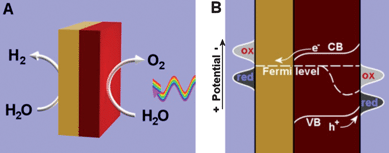 | ||
| Fig. 1 Illustration (A) and energy diagram (B) of a two-electrode water splitting device or particle based water splitting system, in which yellow is metal and red is an n-type semiconductor. Light is incident on the semiconductor from the right. Because of above-band gap light, the holes in the valence band are not in thermal equilibrium with the electrons in the conduction band, which causes the Fermi level to split. The energy levels of the electrolyte are depicted as “red” and “ox”; these levels include water and hydrogen (left) and water and oxygen (right), among the many intermediates formed in the multi-electron transfer process. | ||
Principles of plasmonic effects
The materials and device geometries used in plasmon-enhanced water splitting systems are in many ways familiar. In general, these are nanocomposites of metals and semiconductors. These material combinations have provided improvements in catalysis and charge separation for water splitting systems.4 Unlike these systems, however, the effects that we will describe use metal nanoparticles that strongly interact with frequencies of light corresponding to the solar spectrum.The physical principles that govern plasmons have been described most comprehensively in a classical book,5 and in many recent review articles.6–10 We will therefore only provide a brief introduction here. A central concept in the discussion of localized surface plasmons is that the conduction electrons in a metal nanoparticle act as a harmonic oscillator in response to an oscillating electric field. With an applied electric field, such as that supplied by light, the electron density decreases on one side of the particle and increases on the other. The redistribution of charge creates an electric field inside and outside of the metal nanoparticle that is in the opposite direction of the light's electric field. With the displacement of electron density, there is a coulombic restoring force that begins a series of oscillations in the nanoparticle, much as a spring oscillates once stretched. These coherent oscillations of charge density and electric field are called localized surface plasmons and can continue for about 10 fs,7 at which time the electrons dephase. At 100 fs, electron-electron scattering occurs; producing hot electrons that couple to phonons after about 1 ps. The frequency at which the conduction electrons will oscillate in a metal nanoparticle with minimal power dissipation is called the plasmon resonance frequency. Many metals have plasmon resonances that overlap with the solar spectrum; the resonance frequency can also be engineered by tuning particle size, shape, and environment.11 For solar-to-hydrogen energy conversion applications, however, studies have been limited to silver and gold. This is for several reasons. First, the metal nanoparticles have tuneable plasmon resonances at ultraviolet and visible frequencies.12 Second, they have relatively large optical cross sections – often, 10 times more than their geometric cross section.13 Third, gold is typically stable (thermodynamically or kinetically) under the harsh conditions (pH, potential) that are needed for water splitting.14
Motivations for using plasmonic effects in water splitting
Here we outline some of the challenges facing current state-of-the art water splitting materials and suggest ways in which plasmonic effects can solve these problems. We have identified five areas in which plasmonic effects can help. More details of the physics will be described later.First, many semiconductors that are of interest for water splitting have a short minority carrier distance, L. When L is smaller than the physical size of semiconductor structures in the electrode, bulk recombination of electrons and holes is expected. If the absorption of light can be confined to the near-surface region of a semiconductor so that the distance that minority carriers need to travel is less than L, recombination can be minimized. Plasmonic metal nanoparticles can change the location where charge carriers in the semiconductor are generated by acting as an antenna that localizes the optical energy and transfers it to a semiconductor within approximately 10 nm of the metal.
Second, many semiconductors are too expensive or have low absorption coefficients and it is therefore of interest to use smaller quantities of the semiconductor. There are several ways in which plasmonics can address these challenges. Because metal nanoparticles can act as antennas, smaller amounts of semiconductor are needed to achieve complete light absorption. Moreover, larger metal particles can efficiently scatter light, which increases the path length of light through the semiconductor. Depending on the geometry of the semiconductor, light can be coupled into waveguiding modes or, for semiconductor films that are less than half the wavelength of light, a significant proportion of scattered light can be trapped in the semiconductor by reflecting between its top and bottom surfaces.15
Third, semiconductors that have large bandgaps typically have a low solar-to-hydrogen conversion efficiency because they absorb only a small proportion of solar photons. Plasmonic metal nanoparticles can sensitize the semiconductor to below-band gap light, injecting an excited electron into the conduction band of the semiconductor.
Fourth, many semiconductors have a high refractive index, causing reflection losses from the electrode surfaces. Larger plasmonic metal nanoparticles can decrease this reflection by preferentially scattering the incident light into the film. Reflection can be decreased to a nearly negligible level.
Fifth, to improve charge separation many water splitting devices have high surface areas. Each order of magnitude increase in surface area decreases the obtainable photovoltage by 59 mV.16 This can be understood because the increased surface area dilutes the concentration of minority charge carriers in the near-surface region, thereby altering the Fermi level of minority carriers and, correspondingly, the open circuit photovoltage. Although such devices have not yet been demonstrated, it may be possible to decrease the semiconductor/electrolyte interfacial area to less than the projected surface area, thereby increasing photovoltage in these devices.
Optical, electronic, and catalytic effects of metal particles
In the following section, we address the most prominent chemical, optical, and electronic effects that can arise when a metal nanoparticle is placed at the semiconductor/aqueous interface. An understanding of the mechanisms that can occur when a plasmonic metal nanoparticle is embedded in or near a semiconductor electrode is crucial for distinguishing among possible effects. Fig. 2 provides an illustration of the most relevant processes that can be induced or affected by the presence of a metal nanoparticle when it is placed in direct contact with the semiconductor (Fig. 2A) or separated from the semiconductor by a transparent, insulating spacer (Fig. 2B).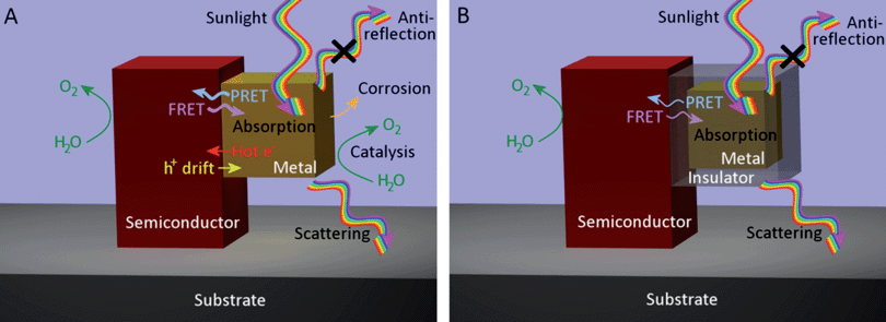 | ||
| Fig. 2 N-type semiconductor nanostructure sitting on a metallic substrate in contact with water and (A) a metal nanoparticle or (B) a core-shell metal-insulator nanoparticle. The most relevant optical, electronic, and catalytic effects of the metal nanoparticle are illustrated in each case. | ||
Light that is incident upon this type of nanocomposite electrode can have many different interactions. Here we briefly outline event sequences; we will focus on the individual processes afterwards. We describe three main sequences based on the first step in the interaction of light with the nanocomposite electrode: (1) absorption by a semiconductor, (2) excitation of a plasmonic resonance, and (3) reflection of light.
In the first sequence, an incident photon is absorbed directly by an n-type semiconductor. This stores the light energy as electrical energy, creating a hole in the valence band and an electron in the conduction band. We will discuss six pathways by which this electrical energy can be transferred or dissipated. Two of these processes are important to mention, although they occur regardless of whether the metal is present: diffusion of the holes to the semiconductor/water interface where water oxidation occurs and trap-mediated recombination of holes with electrons. The remaining four processes are unique to the presence of the metal and will be discussed in greater detail below: Förster Resonant Energy Transfer (FRET), recombination at the metal-semiconductor interface, charge transfer of the hole to the metal followed by water oxidation, and charge transfer of the hole to the metal followed by metal corrosion. (Notably, additional pathways are possible, but will not be discussed because these are not directly related to the presence of the metal).
In the second sequence of events, light energy is transferred to establish a plasmonic resonance in a metal nanoparticle within the nanocomposite electrode. The collective plasmon resonance can follow one of three pathways. The plasmon can be re-radiated (scattered), it can undergo energy transfer to the semiconductor (plasmon resonance energy transfer, PRET), or it can begin a sequence of decay processes that leads to the production of hot electrons. These hot electrons may be injected into the semiconductor or couple to phonons and thermalize. To predict which pathways are most probable, knowledge of the size, shape, and composition-dependent absorption and scattering cross sections of the plasmonic metal nanoparticles is crucial (see Fig. 3). Both theory and experiment have indicated that for spherical gold particles, the scattering cross section becomes larger than the absorption cross section at a particle size of 100 nm.17 This dependence on particle size means that PRET or hot electron production are most probable at small particle sizes and that scattering becomes more probable at large particle sizes.
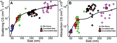 | ||
| Fig. 3 Scattering and absorption cross sections that were calculated from Mie theory (black lines) and determined by the measurement of individual gold nanoparticles. Five sets of nanoparticles with different sizes were used, which corresponds to the five colors of circles. The average value for each set is marked by red squares. Reproduced with permission from the American Chemical Society.17 | ||
In the third sequence of events, light energy is reflected from the electrode surface. Because many semiconductor electrodes have a refractive index of around 3, planar semiconductor electrodes may lose 15% of the incident power.15 As we will discuss further below, the presence of metal nanoparticles can decrease reflection at the metal/semiconductor interface.
Before going into further detail on the optoelectronic and electrochemical processes at metal/semiconductor composite electrodes, it is important to add two additional comments. First, the event sequences described above have been simplified to minimize repetition. Some of these sequences can occur cyclically, such as PRET and FRET.18 Secondly, new physics, are frequently being reported19–21 and therefore it is possible that the event sequences presented here are incomplete.
Plasmon resonance energy transfer (PRET)
The transfer of energy from a plasmon to a nearby absorber, such as a semiconductor, has been called plasmon resonance energy transfer and has stimulated significant interest in several areas beyond solar energy conversion; the same phenomenon is partially responsible for surface enhanced Raman spectroscopy (SERS). The resonating electrons establish an oscillating electric field E; the associated intensity is proportional to E2 and decays from the nanoparticle as 1/d6 at large distances (where d measures the distance from the center of the nanoparticle). At shorter distances, where the curved surface of the plasmonic nanoparticle can be approximated as a flat surface, the decay of the electric field intensity is 1/s4, where s measures the distance from the surface of the nanoparticle. There is also significant variation in the electric field intensity because both photons and plasmons are polarized in a specific direction. Fig. 4 illustrates the electric field intensity for an incident electromagnetic wave near a plasmonic metal nanoparticle in which a dipolar resonance is established. The arrows represent Poynting vectors, i.e., the energy flux of incident light, showing that the metal nanoparticles absorb photons from an area much larger than their geometric cross section.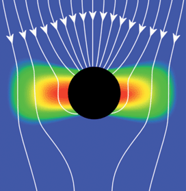 | ||
| Fig. 4 The image illustrates the energy flux (Poynting vectors) that neglect scattering effects and the electric field intensity for an incident electromagnetic wave with an electric field in the plane of the image. Red/blue is high/low electric field intensity. | ||
The spatial distribution of plasmonically excited electrons and holes by PRET depends on the electric field intensity, just as in ordinary photoexcitation. Therefore, knowledge of the electric field intensity associated with the plasmon aids device design. There are several reliable theoretical methods for predicting the electric field intensity; most of these are based on discrete dipole approximation (DDA)22 or finite difference time domain (FDTD) methods.23 Studies that combine simulations with experiments have revealed several principles that have been used to control the electric field intensity, such as the size, shape, and composition of metal nanoparticles. This will be discussed more in the following sections on recent advances and future directions.
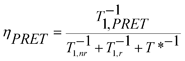
In general, the probability for PRET will be enhanced for metal particles that have low rates of dephasing,24 which is characterized by a time constant T2 or a rate T2−1.25 For this type of system, the dephasing rate is the sum of elastic dephasing (T*−1), radiative decay (T1,r−1), and non-radiative decay (T1,nr−1). T1,nr−1 is the sum of several contributions, which include the rate of interband and intraband generation of electron-hole pairs in the metal and, when the metal is adjacent to an absorbing semiconductor, the rate of PRET, T1,PRET−1.26 The quantum efficiency of PRET is defined as
 | (1) |
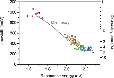 | ||
| Fig. 5 Plasmon dephasing time as a function of resonance energy and nanoparticle size.27 The dephasing time T2 is estimated from the experimentally measured linewidth (Γ) of the plasmon resonance, where Γ = 2ħ/T2. | ||
It has also been stated that the probability of PRET increases with α, the absorption coefficient.9 From our preliminary calculations, it is clear that if efficient PRET- based devices are to be built, semiconductors with relatively high absorption coefficients or short absorption depths (1/α) should be selected. If a threshold light penetration depth of 1 micrometre is chosen, for example, efficient PRET would only be achieved in Si at wavelengths at least below 600 nm,28 in WO3 (monoclinic) at wavelengths below 400 nm,29 in TiO2 (anatase or rutile, undoped) at wavelengths below 330 nm,30 or in a-Fe2O3 (hematite) at wavelengths below 590 nm.31 More details of this model will be forthcoming in future publications. Notably, because the absorption properties of semiconductors are sensitive to preparation conditions, these estimates only provide a guideline for materials selection and device design.
The rate of optical energy absorption by a semiconductor is proportional to the electric field intensity. The effect of PRET is to enhance the electric field intensity in a small, well-defined location of the semiconductor, thereby increasing the power absorbed in this region. In the case of a semiconductor with a short minority carrier transport distance, localizing the dissipation of electromagnetic energy at the semiconductor-water interface provides a way to minimize the average distance that holes must travel to reach the electrolyte. For semiconductors that are limited by majority carrier transport, localizing light absorption near the semiconductor-substrate interface mitigates this limitation.
Scattering and anti-reflection effects
Scattering provides a second mechanism to control the flow of electromagnetic energy in a water splitting device. To maximize the probability of scattering over other effects, particle sizes larger than 100 nm are needed (Fig. 3). Notably, particle sizes larger than 100 nm cause a broadening and damping of the plasmon resonance due to electromagnetic retardation effects.5 This gives rise to more complex scattering patterns from metal nanoparticles, including scattering that occurs in well defined directions due to the increasing scattering cross section of the quadrupolar resonance mode.5The most prominent scattering effect that has been exploited in solar cells is the coupling of scattered light into waveguiding modes or, when the semiconductor layer is much thinner than the wavelength of light, reflection modes.15,33 Scattering occurs preferentially into a material with higher dielectric constant,5,34 and this preferential scattering can be tuned depending on the distance between the dipolar scattering element and the surface.13 This allows the surface scattering element to act as an anti-reflection layer. Calculations predict that as much as 96% of the incident light can be scattered into a semiconductor with a high refractive index.33 It has been noted by several investigators that the presence of an insulating, optically transparent layer between metal and semiconductor is crucial to minimize the damping that can occur when a metal is placed in direct contact with a semiconductor.10,32 In the context of water splitting devices, this spacer should not be continuous so that the electrolyte is in contact with most of the semiconductor surface.
Using these scattering/waveguiding effects, a number of investigators have studied photocurrent enhancements in silicon solar cells. In one of the first studies, a disordered array of metal nanoparticles was placed on top of a p-n semiconductor junction. In this case, an enhancement of up to 80% at 500 nm was achieved.24 In a later version of the device, an overall photocurrent and power enhancement of 8% was achieved under white light illumination.34 In later work, up to a 16-fold enhancement in photocurrent at specific wavelengths was achieved in thin film silicon solar cells that were designed to exploit waveguiding effects. Here, the photocurrent enhancement was seen to vary periodically with wavelength, corresponding to constructive and deconstructive interference in this design.35 An alternative approach has been the exploration of scattering effects in ordered arrays of metals placed at the semiconductor surface. As shown in Fig. 6, metal bars that were placed near a silicon thin film were engineered to achieve a broadband enhancement rather than a periodically oscillating response. An overall white-light enhancement of 40% was achieved in this case. Modeling of the electric field intensity in this device showed that at certain wavelengths, light trapping effects were prominent (Fig. 6B).32
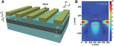 | ||
| Fig. 6 Design of a solar cell employing a plasmonic scattering element that traps the scattered electromagnetic field in reflection modes inside the Si semiconductor. (A) 3-D model and (B) 2-D cross section of the model with a rectangular silver bar. Reproduced with permission from Wiley-VCH.32 | ||
Hot electron/hot hole transfer
If a plasmon is neither emitted as a photon (scattered) nor undergoes PRET, it will be absorbed by the metal nanoparticle, producing hot electrons or holes. If the hot electrons have sufficient energy and are in contact with an n-type semiconductor (Fig. 7), the electrons can be injected into the conduction band of the semiconductor. In this way, the metal nanoparticle acts as a sensitizer to light absorption, in analogy to a dye in a dye sensitized solar cell.36 Although there are few studies on the topic, there is evidence to indicate that the interfacial engineering of the metal-semiconductor contact can play an important role in the design of hot electron creation and injection.37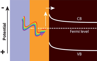 | ||
| Fig. 7 Hot electron injection from a metal into an n-type semiconductor. | ||
For both PRET and light scattering effects, the enhancement will be observed at wavelengths where the plasmon resonance and semiconductor resonance overlap. For hot electron/hot hole transfer injection, enhancements can occur at energies well below the semiconductor band gap.37,38 This provides a key distinguishing characteristic of hot electron/hole transfer.
Förster resonant energy transfer (FRET)
PRET may be considered as a forward reaction of the surface plasmon to excite an electron-hole pair in the semiconductor. FRET, in contrast, is a mechanism by which the excited state in the semiconductor can be quenched by the presence of the metal,39–41 which in the present system can be considered a back reaction. FRET does not involve charge transfer, and can occur over similar length scales to those of PRET. FRET is often depicted as energy transfer from a fluorescent donor (D) to an absorbing acceptor (A).42 The energy transfer rate is a strong function of distance, decaying as d−6 for dipole-donor to dipole-acceptor,42d−5 for nanoparticle donor to nanowire acceptor,41 and d−4 for dipole-donor infinite surface-acceptor,43 where d is the spacing. It is instructive to think about the classical system of energy transfer between two molecules, as this theory serves a basis for analyzing more complicated systems. Between two molecular dipoles,42 the energy transfer rate is | (2) |
 | (3) |
While Förster energy transfer does not involve the emission of a photon, the photoluminescence (PL) of the donor is critical and enters into the energy transfer rate expression both through the quantum yield ηso and the emission spectrum in the overlap integral, fs. In this classical picture, coupling is strongest if both optical transitions are allowed. As eqn (3) indicates, if the donor does not luminesce, then FRET cannot occur. This analysis is somewhat incomplete however. Förster commented on the effect of forbidden transitions on energy transfer.42 For donors, emission from forbidden states can still result in energy transfer because a transition is never strictly forbidden. For acceptors, forbidden absorptions are accounted for in a weak absorption coefficient. Since FRET from the semiconductor to the metal is considered as a quenching mechanism in the present context, it is to be avoided. It is therefore desirable to use semiconductors that have very low rates of radiative recombination. Examples are indirect gap semiconductors and materials where charge separation is much faster than photoemission. Such considerations are encouraging because many functional materials for photoelectrochemical water splitting meet these criteria. As the metal nanoparticle is brought close to the semiconductor to promote PRET, the semiconductor will not be quenched via FRET if it is not photoluminescent.
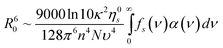
More recent work has developed a theoretical framework for analyzing Förster energy transfer between luminescent nanocrystals and small plasmonic metal nanoparticles (e.g.CdSe).39–41 As expected, there is a strong dependence of FRET on the interparticle spacing, resulting in more quenching at shorter distances (Fig. 8). We note, however, that if luminescent CdSe nanocrystals are incorporated into photoelectrochemical dye sensitized solar cells, the injection of electrons from the excited CdSe nanocrystals into TiO2 quenches over 90% of the PL intensity45 because the injection time is much shorter than the PL lifetime. This suggests a second strategy to minimize FRET by spatially arranging the components such that the electric field within the semiconductor quickly moves photogenerated charges away from the metal nanoparticle. Such strategies have yet to be explored but are potentially important if PRET is to be exploited in high efficiency devices.
 | ||
| Fig. 8 Distance dependence of the energy transfer time from an excited CdSe nanocrystal to a smaller Au nanoparticle. The radius of the Au (RAu) and CdSe (RSNP) nanoparticles are given in the inset. The parameter dexc is the interband dipole moment. The red line is the theoretical curve from the reference, and the blue squares the experimental points from Gueroui et al.44 Reproduced with permission from the American Chemical Society.39 | ||
Catalytic and corrosion effects
As discussed above, there are a number of effects that metal nanoparticles can have on photoelectrochemical systems, beyond optoelectric phenomena. Two such effects are catalytic enhancement and metal corrosion.If we consider an n-type photoanode, the metal nanoparticles on the surface of the semiconductor can lower the overpotential for reactions critical to fuel formation, such as water oxidation. We have demonstrated that Au nanoparticles can be used to shift the onset of photocurrent for water oxidation by Fe2O3 anodes46 indicating a lower overpotential for the reaction. There is an extensive literature on the catalytic effects of metal nanoparticles on electrochemical and photoelectrochemical fuel-forming reactions.47 Our goal here is not to summarize this literature, rather discuss expected effects of catalysis on the measured current-potential (J-V) characteristic of a photoelectrode and its implications for distinguishing plasmonic effects from catalytic or corrosion effects.
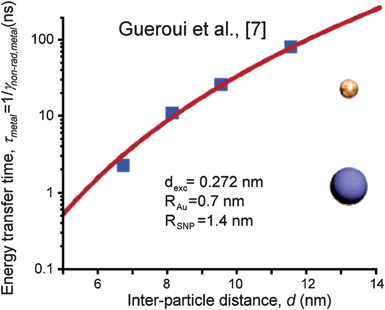
An ideal catalyst will not change the magnitude of photocurrent generated by an electrode (i.e. minority carrier collection), but will shift the onset potential. If one considers an n-type photoanode, a lowering of overpotential will result in a shift of the onset potential in the cathodic direction to more negative potentials. This can result in a similar shape of the J-V curve but it is shifted horizontally to more negative potentials (Fig. 9). If such a shift is observed with no apparent change in the plateau current, then the effect may be catalytic. While such ideal hypothetical behaviour can be used to establish expectations and help interpret results, we note that in reality the situation is more complicated than this. First, the effect of a catalyst can depend on potential, sometimes in non-trivial ways.48 Second, if at high potentials there is surface recombination, the addition of a catalyst has the opportunity to decrease this surface recombination, thereby causing an apparent increase in the plateau photocurrent.49 Additionally, for semiconductors limited by bulk recombination (as in hematite) there is no plateau; rather the form increases as the square root of the difference between the applied potential and the flat band potential.50,51
 | ||
| Fig. 9 Illustrated J-V curves showing a cathodic shift in photocurrent for an n-type photoanode when a catalyst is incorporated. | ||
An additional approach is to identify the potentials at which surface recombination occurs at the semiconductor/electrolyte interface. We recently developed a method for quantifying bulk and surface recombination.49 We used an electrolyte that scavenged holes rapidly, thereby suppressing surface recombination. The resulting J–V curve mimics the effect of an optimally catalyzed photoelectrode for the water splitting process because the main role of a good catalyst is to eliminate surface recombination; i.e., every hole that arrives at the interface is injected into the electrolyte. Comparison of the J–V characteristics for devices with or without a good hole (or electron) scavenging electrolyte allows surface recombination to be quantified across a wide range of potentials.46 In particular, the technique enables potential windows to be identified where surface recombination is completely suppressed. If electrodes modified with metal nanoparticles are studied at these same potentials, any improvement in photocurrent cannot be ascribed to improved catalysis but can possibly be attributed to plasmonic effects.
Photogenerated carriers can also result in photocorrosion of the metal nanoparticles; oxidative potentials used during water splitting can also corrode the metal.14 Corrosion of the metal can have a similar effect as a good catalyst, potentially leading to erroneous conclusions about catalytic effects. There are several ways to differentiate between these effects. The easiest is to determine if a shift in the onset potential is due to corrosion or catalysis by measuring the Faradaic efficiency, i.e. the fraction of the photocurrent that arises from the desired photoelectrochemical reaction. The best way to do this is to quantify the products of the photoreaction as a function of time (e.g. H2 and O2 for water splitting) and calculate the expected production rate from the photocurrent. If fewer products are observed than expected based on the photocurrent, then a side reaction, such as metal corrosion, is occuring. Another simple test is photocurrent stability. If more photocharge passes between the electrodes than would be required to oxidize all of the metal and the photocurrent remains stable, then corrosion cannot be the only photoreaction. These suggestions are given as a starting point, but it is emphasized that the behavior is often system-specific and care must be take to ensure that the metal is stable in order to claim a catalytic effect or rule out a corrosion effect.
Although Pourbaix diagrams14 provide useful guidelines for assessing material stability, it should be noted that the potential experienced by a metal nanoparticle at the surface of a photoelectrode during illumination is different from the externally applied potential. For photoanodes, the quasi Fermi level of holes shifts to positive potentials, leading to a shift in the Fermi level of the metal particle. As demonstrated by Kamat, this can lead to oxidation of gold when placed on TiO2.52
Band bending
The electric field that is established at the semiconductor-water interface separates charge upon light irradiation. Replacing some proportion of this interface by a metal-semiconductor or metal-insulator contact usually changes the band bending within the semiconductor. Several types of effects can be expected, which are all based on the redistribution of charge at the semiconductor interface.When the metal work function is different from the electrochemical potential of the electrolyte solution, band bending occurs to different extents in different regions of the semiconductor. For gold or silver particles on a photoanode, the metal Fermi level is at a more negative potential than the water oxidation potential. This causes a smaller degree of band bending at the metal-semiconductor contact, thereby hindering charge separation. Moreover, if the deposition of metal nanoparticles at the semiconductor surface induces the formation of surface states, Fermi level pinning53 will further decrease band bending within the semiconductor. If surface states are removed or the work function of the metal is more suitably positioned, however, improvements in charge separation can be observed.47
Differing degrees of band bending at the semiconductor-metal and semiconductor-water interface can lead to more complicated effects. For example, there will be additional band bending parallel to the semiconductor surface near the metal-water-semiconductor triple junction.54,55 Additionally, if the mobility of the semiconductor is high and the metal particle size is below 10 nm, potential wells with distinct electronic structure can form.54,55 This has been used to improve the open circuit voltage in photoelectrochemical solar cells.54,55
A unique situation arises for photoelectrodes that are depleted of electrons. This arises when the space charge layer is larger than half of the width of the semiconductor nanostructure.56 Examples often occur in electrodes with low carrier concentrations.57 In these materials, little or no space charge layer exists at the semiconductor-electrolyte interface; the replacement of electrolyte with metal is not expected to change band bending in the semiconductor although this does not preclude the presence of surface states.52
Device geometries
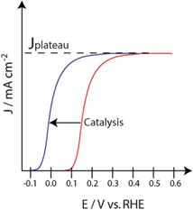
Many of the concepts that inform the design of plasmonic water splitting devices come from research on organic and inorganic solar cells. For the last 20 years, plasmonics have been studied in the context of solar cells and therefore the design of photoelectrochemical (PEC) water splitting devices can gain much from the ways in which these materials have been utilized. We therefore make comparisons between organic and inorganic solar cells systems and look at the impact that these device structures can have on water splitting. It is interesting to note that the most useful geometries for organic and inorganic solar cells are quite different from each other. This allows organic photovoltaics to utilize near-field effects to enhance light absorption, whereas inorganic photovoltaics typically rely on light scattering. Because water splitting devices share structural similarities with both organic and inorganic photovoltaic devices, there are new opportunities in solar water splitting to design solar energy conversion devices that exploit both plasmonic near-field and scattering effects.Organic solar cells (Fig. 10A) typically exploit small plasmonic metal nanoparticles by embedding these particles at the heterojunction where charge separation occurs,58 although other geometries have also been explored.59 This allows light to be localized at the interface between the two phases.
 | ||
| Fig. 10 Device design for solar cells (A, B) and analogous designs for photoelectrochemical cells (C, D). (A) Design of a bulk heterojunction organic solar cell with plasmonic nanoparticles at the heterojunction interface, causing localized exciton formation near the interface. (B) Design of an inorganic solar cell that traps scattered light into the absorbing layer. (C) Design of a photoelectrochemical cell for water splitting that exploits near field carrier generation, which is analogous to (A). (D) Device design for water splitting that is based on light scattering, analogous to (B). In these figures, transparent conducting oxide electrodes are light grey, metal electrodes are dark grey, plasmonic metal nanoparticles are yellow, water is blue, and the semiconductor is red. Regions with an enhanced electric field intensity are depicted in (A) and (C) with color gradients from red (high) to blue (low). | ||
Inorganic solar cells (Fig. 10B), such as those based on silicon p-n junctions, have typically exploited plasmonic nanoparticles located at some distance from the p-n junction. In most cases, the primary mode of operation is by light scattering,60 although some contribution of near-field effects is possible.24
In water splitting devices, the electric field that separates electrons and holes is located at the semiconductor-water interface. Unlike most traditional inorganic solar cells, which have a buried space charge layer, metal nanoparticles can be placed at the semiconductor-water interface, thereby allowing near-field energy transfer from metal to semiconductor in a way that is analogous to organic solar cells. Additionally, scattering effects can be implemented in water splitting devices. Although so far there are no demonstrations of plasmon-enhanced water splitting using plasmonic light scattering, planar geometries would probably be chosen (Fig. 10D), as they have been in the studies of solar cells (Fig. 10C) that exploit light trapping.35
To utilize a near-field enhancement in water splitting, a successful strategy is to minimize the distance that minority carriers must travel.46,61 This can be useful for those circumstances where minority carrier transport is limited either by a low intrinsic mobility or traps. For scattering, metal nanoparticles may be placed at the substrate—semiconductor interface to decrease absorption losses from the metal.9 On the other hand, placement at the back interface may decrease back reflection into the semiconductor. More studies are needed to explore the advantages of these geometries.
Recent advances in plasmon-assisted PEC
Incorporation of metal nanostructures into photoactive semiconductor composites can result in a number of processes that compete for the energy of the incident photon (Fig. 2). These processes can either be beneficial or deleterious to performance of the photoelectrochemical cell. Since plasmon-enhanced photoelectrochemical water splitting is a nascent field in physical chemistry, the parameter space as defined by the materials properties, electrochemical system and illumination conditions has yet to be mapped and so the preliminary reports often contain convoluted results in which the individual effects are difficult to separate. At this early stage, we describe the results of the first papers and emphasize that the goals are to establish design rules and realize a high performance system that has better energy conversion efficiency at the same or lower cost than a conventional system (e.g., PV-electrolyzer or PEC).We will describe the work that has been done on plasmon-PEC water splitting cells by covering the literature in roughly chronological order to illustrate the conceptual development. As previously mentioned, the photophysics of metal nanostructures has been discussed extensively in the physics and chemistry literature over the last century.5 Metal nanoparticles have also been extensively employed as catalysts, and so the reader is referred to that body of literature for reference.47 We focus here on studies that rely on hot electron transfer or plasmon resonance energy transfer to a semiconductor. Aqueous systems are obviously required for direct photoelectrochemical water splitting cells, and photoactivity in the metal is neccesary to realize the theoretical enhancements of plasmonic nanocomposites.
The recent thrust in plasmon-enhanced photoactivity in aqueous semiconductor systems began approximately 7 years ago. Since TiO2 (bandgap, Eg = 3.0 to 3.2 eV) was used as the semiconductor, and visible light activity is necessary for solar energy conversion, the early work focused on hot electron transfer from excited Au and Ag nanoparticles with localized surface plasmon resonances (LSPR) from 400 to 600 nm. The hot electron transfer in the early work is different from more recent work, where energy transfer or absorption enhancements in semiconductors with narrower band gaps (Eg ∼ 2.0 eV) has been studied.
Hot electron transfer enhancements
Tian and Tatsuma published a study in 2004 on the photocurrent and photovoltage action spectra of Au-TiO2 and Ag-TiO2 nanocomposites synthesized by soaking mesoporous TiO2 films in solutions containing 20 nm particles of either Au or Ag.62 The resulting composites were characterized photoelectrochemically under anodic conditions in 0.05 M NaOH solutions (containing 0.5M KI + 0.050 M I2 for photocurrent measurements). For both the Au-TiO2 and Ag-TiO2 composites, the incident photon to current conversion efficiency (IPCE) and photovoltage action spectrum matched the LSPR in the metal nanoparticles, showing a very large increase over the TiO2-only controls in the visible region of the spectrum where TiO2 exhibits no photoactivity. Since the LSPR frequency of Au nanoparticles was at a lower frequency than the TiO2 band gap transition, the behavior was attributed to electron transfer from the photoexcited metal nanoparticles to the TiO2, which was later shown to be accompanied by hole transfer to a species in the electrolyte. In the case of Au, the photocurrent was stable with time, even after passing enough current to oxidize all of the metal. The Ag-TiO2 composite was reported to be less stable than the Au-TiO2 system, which presumably resulted from the Ag being rapidly oxidized under the anodic conditions used for the PEC characterization. From our reading of the literature, this constitutes the first report in the recent work on plasmon enhancement for an energy conversion system containing an aqueous electrolyte.In this first study the absolute values of the enhancements were modest (IPCE = 1.0% at 550 nm in Au-TiO2). This work was followed up by a full paper in 2005 that focused on plasmon-induced electron transfer in the Au-TiO2 system.63 This study was conducted in an acetonitrile/ethylene glycol electrolyte with different electron donors, but is discussed because of its similarity to the aqueous systems reported previously. The Au-TiO2 composite was studied primarily for use in a two-electrode photovoltaic configuration similar to dye-sensitized solar cells. The optimized cell configuration was a Au-TiO2 photoanode, with an acetonitrile-ethylene solvent that contained 0.1 M LiNO3, 0.1 M FeCl2 and 0.05 M FeCl3. This cell produced an open circuit voltage of ∼650 mV, short circuit current of 0.25 mA cm−2 and a fill factor of 50% under white light illumination (λ>420 nm) at an intensity of 10 mW cm−2. The IPCE value at the peak wavelength of the localized surface plasmon resonance (λ = 560 nm) was 12% (Fig. 11). Addition of 0.2 M 4-nitrobenzoic acid to the electrolyte, which was postulated to suppress surface recombination, led to an even higher IPCE of 26%. Because electron–phonon coupling in a metal is strong, plasmons thermalize within a few picoseconds of their generation.25 This makes these results remarkable in that such a large proportion of hot electrons are injected into TiO2 before they thermalize. These results also suggest that plasmonic metal nanoparticles can be used in analogy to dyes in a dye sensitized solar cell.
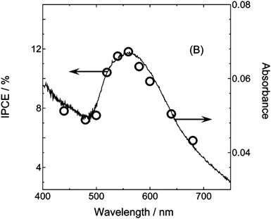 | ||
| Fig. 11 Correspondence of plasmonic resonance and the enhancement in photocurrent in mesoporous Au-TiO2 nanocomposites. Reproduced with permission from the American Chemical Society.63 | ||
Hot electron transfer from gold nanoparticles has also been studied using femtosecond spectroscopy.64 In these measurements, the laser intensity is sufficiently high that thousands of photons are absorbed per gold nanoparticle during a single laser pulse, which may result in significantly different dynamics than occur under solar irradiation. Nevertheless, a 40% yield for hot electron injection from Au nanoparticles into TiO2 was observed,64 which is similar to the 26% yield reported for lower illumination intensity.63 The authors found that hot electrons are injected into TiO2 within 240 fs of excitation, which was the shortest time scale that could be measured.64 As noted by the authors, it was not possible to determine the mechanism of hot electron injection.
Several studies have been conducted on the effect of small Au nanoparticles on the visible light activity of TiO2-based photocatalysts for organic decontamination. In contrast to photoelectrochemical systems, in these photocatalytic systems the photoactive species are not connected to an external circuit, and instead the chemical products of a degradation reaction are monitored as a function of time under illumination. Such systems are briefly mentioned here because the reactions are conducted in aqueous systems and could therefore be relevant to plasmon-enhanced photoelectrochemical water splitting.
Research on LSPR-driven photocatalytic activity has focused largely on the Au-TiO2 system. Enhancements in visible light reactivity are expected because of hot electron transfer driven by the photoexcited Au nanoparticles. This work has been reviewed recently by Primo, Corma and García,65 so the discussion here will be brief. It is well known that small Au nanoparticles have different catalytic properties than the bulk,66 which re-emphasizes the challenge of deconvoluting and isolating plasmonic effects. Increases in activity of the Au-TiO2 composite photocatalyst over a TiO2 control cannot be taken alone as evidence of a plasmon enhancement because of possible catalytic effects. The simplest test for hot electron transfer is photoactivity in a region of the illumination spectrum where there is no activity in the TiO2 control. Stronger evidence can be obtained by comparing the action spectrum to the LSPR absorbtion spectrum. Such observations have been made by Rodríguez-González et al. in 200767 and Kowalska et al. in 2008.68 Rodríguez-González et al. observed an increase in the degradation rate of methyl tert-butyl ether (MTBE) in water for Au-TiO2 compared to TiO2 under visible illumination from a krypton lamp that had strong emission lines at the LSPR peak wavelength, which is consistent with electron injection into the TiO2.67 However, the most active composite was the Au-TiO2-Al2O3 photocatalyst, for which no LSPR absorbance could be measured. As a result, the presence of a plasmonic enhancement in this system is difficult to assess.
The reports of Kowalska et al. in 200968 and 201069 provide stronger evidence for an LSPR enhancement in the Au-TiO2 photocatalytic system. The authors measured the action spectrum of isopropanol oxidation in water as a function of illumination wavelength. While the peak quantum efficiencies in the visible portion of the spectrum were low (∼0.03%), they were much higher than the TiO2-only controls and the peak wavelength coincided with the peak wavelength of the LSPR as determined from the absorption spectra. The authors proposed the following dominant mechanism: excitation of the LSPR in the Au nanoparticles results in electron injection into the TiO2 conduction band, eventually reducing dissolved oxygen while the Au nanoparticle oxidizes the isopropanol. The hot electron mechanism and the evidence to support it are consistent with the observations of Tian and Tatsuma.
Building on these results, Primo et al. published a photocatalytic study in February of 2011 where they demonstrated enhanced water photooxidation on Au-CeO2 nanocomposites using Ag+ as a sacrificial electron acceptor at wavelengths corresponding to the peak wavelength of the Au LSPR.70 Under UV illumination, the CeO2 band gap transition was directly excited and the resulting hole oxidized water and the electron was captured by Ag+. Under UV illumination, the Au had no effect on the activity of the CeO2 at low loadings (1.0 wt % Au) and a detrimental effect at high loadings (3.0 wt % Au). The Au acted as an electron trap, promoting recombination with the photogenerated hole and therefore lowering the water oxidation rate. This explanation is consistent with results that will be presented in the following section. Under visible illumination (λ > 400 nm), the CeO2 alone exhibits no activity for water oxidation but the Au-CeO2 composites achieve higher water oxidation rates than the CeO2 exhibits under UV illumination, clearly illustrating the enhancement due to the plasmon excited in the Au nanoparticle. The hot electron transfer mechanism was invoked to explain the result because absorption at visible frequencies by CeO2 is negligible.
PRET enhancements
More recent work sought to elucidate the role of PRET in photoelectrochemical water splitting. We describe two studies focused on water oxidation in systems where such an energy transfer mechanism might be expected, but where the authors do not claim a particular mechanism. We then move on to more recent studies in which the authors invoke such a mechanism to explain their results.In 2009, Jang et al. reported on the photooxidation of water by Sn4+-doped Ag-Fe2O3 nanocomposite photoanodes.71 This work was a scanning electrochemical microscopy study looking at compositional effects, and was not presented in the context of plasmonics, but will be briefly mentioned here because it involved metallic Ag. The authors report that the optimum composition for the parameters they investigated was Sn4+-doped Ag-Fe2O3 with an Ag:Fe ratio of 1 and a Sn4+ concentration of 2%. The Ag in the electrode was reported to be in the form of metallic nanoparticles. The highest performing electrode generated a photocurrent of approximately 0.13 mA cm−2 in a 0.2 M NaOH electrolyte at 0.6 V vs.Ag/AgCl under visible illumination by a 150 W Xe lamp (λ > 420nm) and was reported to have good stability.
In late 2010, Solarska et al.72 published a communication reporting enhanced photoelectrochemical water oxidation by Ag-WO3 nanocomposites. The Ag nanoparticles were synthesized by thermal evaporation to produce ultrathin particles corresponding to a mass thickness of 2 to 4 nm. This was followed by the deposition of a 1 micron-thick mesoporous WO3 film. Before deposition of WO3, the maximum plasmonic extinction was 0.075 (corresponding to a transmittance of 85%); this further decreased upon addition of the WO3, consistent with theoretical predictions.32 Indeed, for some samples, no increase in absorption at the plasmon resonance was observed after WO3 deposition. In spite of the small influence of the plasmonic absorption, the authors attribute the 10 to 20% increase in IPCE at 1.5 V/RHE upon addition of Ag to a plasmonic effect. The enhancement was also observed under AM1.5 illumination (100 mW cm−2) in a 1 M H2SO4 electrolyte, where a photocurrent of 1.8 mA cm−2 was achieved at approximately 1.0 V vs.RHE, much higher than the WO3 control which only produced 1.3 mA cm−2 under the same conditions. Notably, the photocurrent onset shifted in the cathodic direction by 200 mV upon incorporation of the Ag nanoparticles, which suggests that the role of the silver particles is either catalytic or as a hole acceptor, especially since at these potentials and pHs silver rapidly dissolves.14 This is consistent with the observation that the enhancement was diminished when the silver was protected from the electrolyte. As suggested by the authors, the improvements in photocurrent can also be explained by changes in light scattering or reflection.
In December 2010, we published a report on the influence of plasmonic Au nanoparticles on water photooxidation performance when the Au was embedded in compact Fe2O3 thin films and placed on the surface of Fe2O3 nanoplatelets.46 The compact and nanoplatelet Fe2O3 controls produced photocurrents of 0.4 mA cm−2 and 2.0 mA cm−2 respectively at 1.4 V/RHE under simulated AM1.5 illumination (100 mW cm−2), illustrating how minority carrier collection can be improved by nanostructuring in the nanoplatelet case. In both configurations, when the Au nanoparticles (50 nm diameter) were embedded in the compact Fe2O3 thin films or on the surface of the nanoplatelets, the overall photocurrent went down due to reduced photovoltage, presumably a result of enhanced recombination at the Au-Fe2O3 interface. In the configuration with Au nanoparticles deposited on the surface of the Fe2O3 nanoplatelets, a relative increase in the normalized IPCE spectra was observed in the region of overlap between the LSPR and Fe2O3 absorption, consistent with PRET (Fig. 12). No such change in the normalized IPCE spectrum was observed when the Au nanoparticles were embedded in a 31 nm compact Fe2O3 thin film because the LSPR frequency was redshifted to 670 nm, a lower frequency than the Fe2O3 band gap transition at approximately 590 nm (∼2.1 eV). In the work, we were able to separate the influence of PRET from light scattering, catalysis, hot electron, and band bending effects at the semiconductor-metal interface. We identified that surface states at the Au-Fe2O3 interface produce traps and promote recombination. We indicated that shells that are chemically inert, prevent charge transfer, and are optically transparent (e.g.SiO2) might be used to electrically isolate Au from the Fe2O3, to allow PRET without forming recombination centers.
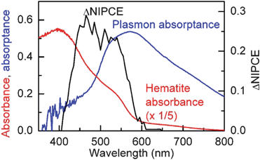 | ||
| Fig. 12 Hematite absorbance (red) for 300 nm nanoplatelets on FTO and plasmon absorptance of 45 nm Au nanoparticles in the surface configuration. The difference in the normalized IPCE between the Fe2O3-only control and Au-Fe2O3 electrode is plotted in black. A relative enhancement is observed only at wavelengths where the LSPR and semiconductor absorbance overlap. Reproduced with permission from the American Chemical Society.46 | ||
In March 2011, Thomann et al. published a study on arXiv (later republished in Nano Letters), where Au nanoparticles with and without SiO2 shells were placed on the surface of, and embedded in, compact Fe2O3 thin films that were then used for photooxidation of water.61 The compact Fe2O3 controls produced photocurrents of approximately 0.1 mA cm−2 at 1.4 V/RHE under white light illumination (∼100 mW cm−2). The authors observed the highest photocurrent enhancement in the configuration where SiO2-coated Au nanoparticles were annealed on the surface of the compact Fe2O3 films. Under these conditions, a wavelength-independent enhancement of unknown origin of 5 to 8 times was observed over the Fe2O3-only sample (Fig. 13). Superimposed on this enhancement was a second enhancement centered at 600 nm, which is just beyond the hematite band edge. The relative enhancement in photocurrent at wavelengths around 600 nm is consistent with a plasmonic near-field effect, although it is on the order of tens of nA cm−2 since the IPCE of the hematite-only control is <0.01%. If PRET contributes to the enhancement mechanism, this is most likely based on the excitation of electrons from surface traps to the conduction band, since much of the enhancement occurs at energies below the band gap energy. Although a microporous 2-nm silica shell surrounds the gold nanoparticles, there may also be a small contribution from hot electron transfer to the sub-band gap photocurrent because the plasmon density of states is known to extend well outside the metal nanoparticle surface.74 The low photocurrents and unknown origin of the largest photocurrent enhancement make it hard to distinguish possible mechanisms. The use of an enhancement factor has also been critiqued73 because it does not report the photocurrent or IPCE, which is needed to assess the viability of a synthetic approach.
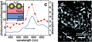 | ||
| Fig. 13 Device geometry (inset, left), photoresponse (left) and SEM image (right) of gold-silica core-shell nanoparticles on a flat hematite electrode. Reproduced with permission from the American Chemical Society.61 | ||
In early 2011, two studies on plasmon-enhanced, nitrogen-doped titanium dioxide (N-TiO2) photoanodes were published. N-TiO2 has been extensively explored for photocatalysis and photoelectrochemical oxidation because of its ability to red-shift absorption to visible frequencies, making it a more attractive solar absorber than pristine TiO2 that only responds to photons of less than 400 nm in wavelength. For clarity, we address these in reverse chronological order.
In March of 2011, Ingram and Linic published a study where the photoelectrochemical water oxidation performance of nanocomposite Ag/N-TiO2 electrodes was compared to Au/N-TiO2.73 The N-TiO2 responded to wavelengths less than 500 nm, and produced rather modest overall photocurrents of several μA cm−2 under illumination from 400 nm to 900 nm at an intensity of 500 mW cm−2. The Ag nanoparticles were cubes, 120 nm on a side with LSPR peaks at approximately 410 nm and 580 nm (Fig. 14); while the Au nanoparticles were spherical and 25 nm in diameter with peak wavelengths of approximately 520 nm and 680 nm. The authors observed an increase in reaction rate for the Ag nanoparticles at wavelengths less than 500 nm, but not for Au. The authors attributed the enhancement with Ag to energy transfer from the metal to the semiconductor due to the overlap in the LSPR frequency of the Ag and the absorbance of the N-TiO2. Since the LSPR in the Au case was at a lower frequency than the absorption onset of the N-TiO2, no enhancement was observed. The observation of an enhancement with Ag when there was spectral overlap with the semiconductor absorption, and the lack of an enhancement with Au when there was no overlap, is consistent with a PRET mechanism enhancing excitation of the N-TiO2 in the vicinity of the metal nanoparticle. Importantly, the authors also suggested that certain polymeric stabilizers such as poly(vinylpyrrolidone) can suppress FRET. More work in this area would be clearly beneficial to achieve higher water oxidation rates through suppression of excitation quenching. Overall, the work of Ingram and Linic provides strong evidence that there must be absorption overlap between the semiconductor and LSPR for energy transfer to result in preferential excitation of the semiconductor in the vicinity of the metal nanoparticle.
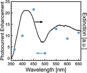 | ||
| Fig. 14 Photocurrent enhancement factor (photocurrent of Ag/N-TiO2 composite divided by N-TiO2 composite) and optical extinction spectrum. As noted by the authors, caution is needed in interpreting photocurrent enhancements.73 Reproduced with permission from the American Chemical Society.73 | ||
Liu et al. published a report in February of 2011 on the effect of discontinuous films prepared during the initial island-growth stage of Au deposition onto anodized TiO2.75 The as-prepared anodic TiO2 (ATO) exhibited photoactivity at wavelengths less than approximately 620 nm, presumably a result of impurity incorporation during synthesis that introduced sub-gap states that can promote the water oxidation reaction. The overall performance of the unmodified ATO was low, exhibiting photocurrents of approximately 5 μA when illuminated at 532 nm with an intensity of 7000 mW cm−2. A clear increase in photocurrent at wavelengths corresponding to the plasmon resonance was observed. The increase was explained to be a result of PRET, which was supported by FDTD calculations that integrated the spatial distribution of the electric field intensity enhancement over an assumed 1 minority carrier diffusion length away from the metal nanostructure.
In this section we have covered the recent reports of plasmon enhancement in photoelectrochemical and photocatalytic systems relevant to photo water splitting. It is clear that this subfield of physical chemistry is in its nascent stages, and much more research on understanding fundamental behavior will be required to achieve high performance through advanced photon management in the photoelectrochemical systems.
Future directions
Plasmon enhancements are an exciting route to control the flow of electromagnetic energy in photocatalytic and photoelectrochemical water splitting devices. PRET enables precise spatial control over photon absorption in a semiconductor. This approach is especially useful in materials where photocurrent is limited by a short minority carrier transport distance, although the full range of advantages of PRET has yet to be explored. Many emerging semiconductors that are of both scientific and economic interest, such as hematite, are excellent candidates for studying plasmonic effects because these same semiconductors often have high defect densities that promote recombination. PRET may also provide advantages for more expensive or rare semiconductors by reducing the amount of semiconductor required for photoabsorption. Through plasmonics, it may be possible to absorb approximately the same amount of light using 3 orders of magnitude less semiconductor,76 effectively concentrating the light and increasing the photovoltage and efficiency. It may even be possible to fabricate a device with a smaller semiconductor-electrolyte interfacial area than the projected area of the substrate, leading to dramatic increases in photovoltage.At this stage these ideas are primarily proposals. A high performance system relevant for societal-level solar energy conversion based on these effects has not yet been demonstrated. The goal is to demonstrate an enhancement over a state-of-the-art conventional device. Moreover, realistic implementation of these materials will require the use of earth-abundant, inexpensive metal nanoparticles such as copper and aluminum. Methods to achieve stability of these materials in aqueous environments under oxidative conditions are needed.
Although theoretical studies, especially those incorporated finite difference time domain studies can be illuminating, an important direction in future research will be to model the disordered arrays of metal and semiconductor that are most likely to be implemented in future devices. At the same time, simple and efficient synthetic methods that can achieve precise structural control over nanoparticle placement and geometry in nanocomposite arrays may be crucial for maximizing the electric field intensity enhancements that are crucial to PRET. The use of conformal, pin-hole free photoactive coatings of materials with a good match to both the LSPR and solar spectrum is also important. Atomic layer deposition is well suited to the task, and a forthcoming article will discuss the role that this process can play both in the synthesis of ultrathin solar absorbers and photoelectrochemical water splitting in general. Additionally, explorations of water splitting using surface plasmon polaritons may result in advantageous effects, as demonstrated in solar cells.77
Plasmonic water splitting is a fertile new field in physical chemistry, and there is a multitude of basic work that must be carried out to characterize the governing behavior in relevant experimental systems. The first results are encouraging, and a framework has been established to interpret results. Thus the groundwork has been laid to make a breakthrough by advanced photon management in one of the most important application areas of our time: solar fuel production.
Notes and references
- J. Goldemberg and T. B. Johansson, World Energy Assessment: Overview 2004 Update, United Nations Development Programme, New York, 2004 Search PubMed.
- J. A. Turner, Science, 1999, 285, 687–689 CrossRef CAS.
- N. S. Lewis and G. Crabtree, Basic Research Needs for Solar Energy Utilization, U.S. Department of Energy Office of Science, 2005 Search PubMed.
- A. J. Bard and M. A. Fox, Acc. Chem. Res., 1995, 28, 141–145 CrossRef CAS.
- U. Kreibig and M. Vollmer, Optical Properties of Metal Clusters, Springer, Berlin, 1995 Search PubMed.
- L. M. Liz-Marzán, Langmuir, 2006, 22, 32–41 CrossRef.
- G. V. Hartland, Chem. Rev., 2011, 111, 3858–3887 CrossRef CAS.
- N. J. Halas, S. Lal, W.-S. Chang, S. Link and P. Nordlander, Chem. Rev., 2011, 111, 3913–3961 CrossRef CAS.
- H. A. Atwater and A. Polman, Nat. Mater., 2010, 9, 205–213 CrossRef CAS.
- J. A. Schuller, E. S. Barnard, W. Cai, Y. C. Jun, J. S. White and M. L. Brongersma, Nat. Mater., 2010, 9, 193–204 CrossRef CAS.
- M. Rycenga, C. M. Cobley, J. Zeng, W. Li, C. H. Moran, Q. Zhang, D. Qin and Y. Xia, Chem. Rev., 2011, 111, 3669–3712 CrossRef CAS.
- A. Boltasseva and H. A. Atwater, Science, 2011, 331, 290–291 CrossRef CAS.
- K. R. Catchpole and A. Polman, Appl. Phys. Lett., 2008, 93, 191113 CrossRef.
- M. Pourbaix, Atlas of electrochemical equilibria in aqueous solutions, Cebelcor, Houston, 1974 Search PubMed.
- B. E. A. Saleh and M. C. Teich, Fundamental of Photonics, John Wiley and Sons, Hoboken, New Jersey, 2007 Search PubMed.
- M. G. Walter, E. L. Warren, J. R. McKone, S. W. Boettcher, Q. Mi, E. A. Santori and N. S. Lewis, Chem. Rev., 2010, 110, 6446–6473 CrossRef CAS.
- A. Tcherniak, J. W. Ha, S. Dominguez-Medina, L. S. Slaughter and S. Link, Nano Lett., 2010, 10, 1398–1404 CrossRef CAS.
- A. O. Govorov, G. W. Bryant, W. Zhang, T. Skeini, J. Lee, N. A. Kotov, J. M. Slocik and R. R. Naik, Nano Lett., 2006, 6, 984–994 CrossRef CAS.
- M. A. Noginov, G. Zhu, A. M. Belgrave, R. Bakker, V. M. Shalaev, E. E. Narimanov, S. Stout, E. Herz, T. Suteewong and U. Wiesner, Nature, 2009, 460, 1110–1112 CrossRef CAS.
- R. F. Oulton, V. J. Sorger, T. Zentgraf, R.-M. Ma, C. Gladden, L. Dai, G. Bartal and X. Zhang, Nature, 2009, 461, 629–632 CrossRef CAS.
- M. Artamonov and T. Seideman, Nano Lett., 2010, 10, 4908–4912 CrossRef CAS.
- B. T. Draine and P. J. Flatau, J. Opt. Soc. Am. A, 1994, 11, 1491–1499 CrossRef.
- A. Taflove and M. E. Browdin, IEEE Trans. Microwave Theory Tech., 1975, 23, 623–630 CrossRef.
- D. M. Schaadt, B. Feng and E. T. Yu, Appl. Phys. Lett., 2005, 86, 063106 CrossRef.
- E. J. Heilweil and R. M. Hochstrasser, J. Chem. Phys., 1985, 82, 4762 CrossRef CAS.
- C. Sönnichsen, T. Franzl, T. Wilk, G. von Plessen, J. Feldmann, O. Wilson and P. Mulvaney, Phys. Rev. Lett., 2002, 88, 077402 CrossRef.
- C. Sönnichsen, T. Franzl, T. Wilk, G. von Plessen and J. Feldmann, New J. Phys., 2002, 4, 93 CrossRef.
- W. C. Dash and R. Newman, Phys. Rev., 1955, 99, 1151 CrossRef CAS.
- C. Santato, M. Odziemkowski, M. Ulmann and J. Augustynski, J. Am. Chem. Soc., 2001, 123, 10639–10649 CrossRef CAS.
- G. Jellison, L. Boatner, J. Budai, B. Jeong and D. Norton, J. Appl. Phys., 2003, 93, 9537 CrossRef CAS.
- L. A. Marusak, R. Messier and W. B. White, J. Phys. Chem. Solids, 1980, 41, 981–984 CrossRef CAS.
- R. A. Pala, J. White, E. Barnard, J. Liu and M. L. Brongersma, Adv. Mater., 2009, 21, 3504–3509 CrossRef CAS.
- K. R. Catchpole and A. Polman, Opt. Express, 2008, 16, 21793–21800 CrossRef CAS.
- D. Derkacs, S. H. Lim, P. Matheu, W. Mar and E. T. Yu, Appl. Phys. Lett., 2006, 89, 093103 CrossRef.
- S. Pillai, K. R. Catchpole, T. Trupke and M. A. Green, J. Appl. Phys., 2007, 101, 093105–093108 CrossRef.
- B. O'Regan and M. Grätzel, Nature, 1991, 353, 737 CrossRef CAS.
- M. W. Knight, H. Sobhani, P. Nordlander and N. J. Halas, Science, 2011, 332, 702–704 CrossRef CAS.
- Y. Tian and T. Tatsuma, J. Am. Chem. Soc., 2005, 127, 7632–7637 CrossRef CAS.
- A. O. Govorov, G. W. Bryant, W. Zhang, T. Skeini, J. Lee, N. A. Kotov, J. M. Slocik and R. R. Naik, Nano Lett., 2006, 6, 984–994 CrossRef CAS.
- A. O. Govorov, J. Lee and N. A. Kotov, Phys. Rev. B: Condens. Matter Mater. Phys., 2007, 76 CrossRef CAS.
- A. O. Govorov and P. L. Hernandez-Martinez, Phys. Rev. B: Condens. Matter Mater. Phys., 2008, 78, 035314 CrossRef.
- T. Forster, Discuss. Faraday Soc., 1959, 27, 7–17 RSC.
- C. A. Grimes, J. I. Basham and G. K. Mor, ACS Nano, 2010, 4, 1253–1258 CrossRef.
- Z. Gueroui and A. Libchaber, Phys. Rev. Lett., 2004, 93 CrossRef CAS.
- A. Kongkanand, K. Tvrdy, K. Takechi, M. Kuno and P. V. Kamat, J. Am. Chem. Soc., 2008, 130, 4007–4015 CrossRef CAS.
- E. Thimsen, F. Leformal, M. Graetzel and S. C. Warren, Nano Lett., 2011, 11, 35–43 CrossRef CAS.
- P. V. Kamat, J. Phys. Chem. B, 2002, 106, 7729–7744 CrossRef CAS.
- J. K. Norskov, J. Rossmeisl, A. Logadottir, L. Lindqvist, J. R. Kitchin, T. Bligaard and H. Jonsson, J. Phys. Chem. B, 2004, 108, 17886–17892 CrossRef CAS.
- H. Dotan, K. Sivula, M. Graetzel, A. Rothschild and S. C. Warren, Energy Environ. Sci., 2011, 4, 958–964 CAS.
- W. W. Gärtner, Phys. Rev., 1959, 116, 84–87 CrossRef.
- H. S. Jarrett, J. Appl. Phys., 1981, 52, 4681–4689 CrossRef CAS.
- V. Subramanian, E. Wolf and P. V. Kamat, J. Phys. Chem. B, 2001, 105, 11439–11446 CrossRef CAS.
- A. J. Bard, A. B. Bocarsly, F. R. F. Fan, E. G. Walton and M. S. Wrighton, J. Am. Chem. Soc., 1980, 102, 3671–3677 CrossRef CAS.
- Y. Nakato and H. Tsubomura, J. Photochem., 1985, 29, 257–266 CrossRef CAS.
- Y. Nakato, T. Ohnishi and H. Tsubomura, Chem. Lett., 1975, 4, 883–886 CrossRef.
- J. W. Orton and M. J. Powell, Rep. Prog. Phys., 1980, 43, 1263–1307 CrossRef.
- M. Gratzel, Nature, 2001, 414, 338–344 CrossRef CAS.
- A. J. Morfa, Appl. Phys. Lett., 2008, 92, 013504 CrossRef.
- O. Stenzel, A. Stendal, K. Voigtsberger and C. von Borczyskowski, Sol. Energy Mater. Sol. Cells, 1995, 37, 337–348 CrossRef CAS.
- H. R. Stuart and D. G. Hall, Appl. Phys. Lett., 1998, 73, 3815 CrossRef CAS.
- I. Thomann, B. A. Pinaud, Z. B. Chen, B. M. Clemens, T. F. Jaramillo and M. L. Brongersma, Nano Lett., 2011, 11, 3440–3446 CrossRef CAS.
- Y. Tian and T. Tatsuma, Chem. Commun., 2004, 1810–1811 RSC.
- T. Tatsuma and Y. Tian, J. Am. Chem. Soc., 2005, 127, 7632–7637 CrossRef.
- A. Furube, L. Du, K. Hara, R. Katoh and M. Tachiya, J. Am. Chem. Soc., 2007, 129, 14852–14853 CrossRef CAS.
- A. Primo, A. Corma and H. Garcia, Phys. Chem. Chem. Phys., 2011, 13, 886–910 RSC.
- P. Mulvaney, R. Sardar, A. M. Funston and R. W. Murray, Langmuir, 2009, 25, 13840–13851 CrossRef.
- V. Rodriguez-Gonzalez, R. Zanellac, G. del Angela and R. Gomeza, J. Mol. Catal. A: Chem., 2008, 281, 93–98 CrossRef CAS.
- E. Kowalska, R. Abe and B. Ohtani, Chem. Commun., 2009, 241–243 RSC.
- E. Kowalska, O. O. P. Mahaney, R. Abe and B. Ohtani, Phys. Chem. Chem. Phys., 2010, 12, 2344–2355 RSC.
- H. Garcia, A. Primo, T. Marino, A. Corma and R. Molinari, J. Am. Chem. Soc., 2011, 133, 6930–6933 CrossRef.
- A. J. Bard, J. S. Jang, K. Y. Yoon, X. Y. Xiao and F. R. F. Fan, Chem. Mater., 2009, 21, 4803–4810 CrossRef.
- R. Solarska, A. Krolikowska and J. Augustynski, Angew. Chem., Int. Ed., 2010, 49, 7980–7983 CrossRef CAS.
- D. B. Ingram and S. Linic, J. Am. Chem. Soc., 2011, 133, 5202–5205 CrossRef CAS.
- J. Nelayah, M. Kociak, O. Stephan, F. J. Garcia de Abajo, M. Tence, L. Henrard, D. Taverna, I. Pastoriza-Santos, L. M. Liz-Marzan and C. Colliex, Nat. Phys., 2007, 3, 348–353 CrossRef CAS.
- Z. W. Liu, W. B. Hou, P. Pavaskar, M. Aykol and S. B. Cronin, Nano Lett., 2011, 11, 1111–1116 CrossRef CAS.
- C. Hagglund, S. P. Apell and B. Kasemo, Nano Lett., 2010, 10, 3135–3141 CrossRef CAS.
- V. E. Ferry, L. A. Sweatlock, D. Pacifici and H. A. Atwater, Nano Lett., 2008, 8, 4391–4397 CrossRef CAS.
| This journal is © The Royal Society of Chemistry 2012 |