Enhancement of thermoelectric figure-of-merit by resonant states of aluminium doping in lead selenide
Qinyong
Zhang
ab,
Hui
Wang
b,
Weishu
Liu
b,
Hengzhi
Wang
b,
Bo
Yu
b,
Qian
Zhang
b,
Zhiting
Tian
c,
George
Ni
c,
Sangyeop
Lee
c,
Keivan
Esfarjani
c,
Gang
Chen
*c and
Zhifeng
Ren
*b
aSchool of Material Science and Engineering, Xihua University, Chengdu, Sichuan 610039, P. R. China
bDepartment of Physics, Boston College, Chestnut Hill, Massachusetts 02467, USA. E-mail: renzh@bc.edu; Fax: +1-617-552-8478; Tel: +1-617-552-2832
cDepartment of Mechanical Engineering, Massachusetts Institute of Technology, Cambridge, Massachusetts 02139, USA. E-mail: gchen2@mit.edu; Fax: +1-617-324-5519; Tel: +1-617-253-0006
First published on 11th November 2011
Abstract
By adding aluminium (Al) into lead selenide (PbSe), we successfully prepared n-type PbSe thermoelectric materials with a figure-of-merit (ZT) of 1.3 at 850 K. Such a high ZT is achieved by a combination of high Seebeck coefficient caused by very possibly the resonant states in the conduction band created by Al dopant and low thermal conductivity from nanosized phonon scattering centers.
Broader contextThermoelectric devices directly convert heat to electricity, thus they are important for harvesting natural heat as well as waste heat. For efficient devices, high figure-of-merit (ZT) materials are desired. We report here n-type lead selenide (PbSe) thermoelectric materials with a ZT of 1.3 at 850 K. These materials are prepared by adding aluminium (Al) in PbSe during ball milling and hot pressing. Al, as a dopant in PbSe, possibly creates resonant states in the conduction band and causes increase in the local density of states (DOS) near the Fermi level. As a result, the Seebeck coefficients of Al added PbSe samples are about 40–100% higher than the predicted values by the simple parabolic band model and about 40% higher than the Cl-doped reference PbSe sample without resonant states. Furthermore, using the ball milling and hot pressing technique, the structure of our samples contains features such as Pb depleted discs, small grains, and ∼10 nm subgrains that are effective for phonon scattering, and result in a much lower lattice thermal conductivity of 0.6–0.7 W m−1 K−1 at 850 K. Further improvement could be expected by even better control of the Fermi level through optimization of addition of other doping materials. |
Thermoelectric (TE) materials and devices have drawn significant interest and attention for the past decades due to their potential applications in converting solar energy and waste heat into electricity.1 The performance of thermoelectric materials depends on dimensionless figure-of-merit, ZT = S2σT/(κlat + κcarr), where S, σ, T, κlat, and κcarr are Seebeck coefficient, electrical conductivity, absolute temperature, lattice thermal conductivity, and electronic thermal conductivity, respectively.2 Improvements on ZT can be achieved by either increasing the power factor (S2σ) or reducing the thermal conductivity, or even better, by simultaneously increasing the power factor and reducing the thermal conductivity.3 Potential ways to improve the power factor are through increasing the Seebeck coefficient (S) via band modification4 or engineering,5 energy barrier filtering,6–8 additional carrier pocket,9 and resonant states,10 or enhancing the mobility such as modulation doping.11 Among these possibilities, resonant states and additional carrier pockets have led to net increased ZT values via the power factor enhancements.9,10 In contrast, many methods have been found to be effective in reducing lattice thermal conductivity, for example, alloy scattering, boundary scattering, nanocomposites or nanoinclusion routes, etc. Simultaneously achieving resonant states to enhance the Seebeck coefficient thus the power factor and nanoscale grain boundary scattering to reduce the lattice thermal conductivity have not been reported before.
As one of the most studied bulk TE materials, PbTe based materials received a significant enhancement recently by introducing various nanoinclusions or modifying the band structure, and reached a high ZT value of 1.5–1.8, such as p-type PbTe1−xSex:Na (∼1.8),5PbTe–Sr2Te:Na (∼1.7),12PbTe:Tl (∼1.5),4,6 NaPbmSbTe2+m (∼1.7),13 and n-type AgPbmSbTe2+m (∼1.7)14 and PbTe–PbS:PbI2(∼1.5).15 All these materials are based on Te. However, Te is extremely rare in the earth crust, just 0.001 ppm, which is even less than 0.004 ppm for Au and 0.005 ppm for Pt. This will limit the wide applications of PbTe-based materials. To develop materials without Te or less Te will be very urgent and important. Although PbS and PbSe are very similar to PbTe in crystal structure, band structure, and many other properties,17 they are much less studied than PbTe because of the concerns that the smaller size of S or Se and lighter atomic mass in comparison with Te potentially result in higher lattice thermal conductivity.
Recently, a theoretical calculation on PbSe by Parker and Singh16 showed that due to the flat feature of the energy diagram in the valence band, the p-type PbSe possibly reach ZT ≈ 2 at 1000 K if it is heavily doped. Based on this suggestion, Wang et al. doped Na into PbSe,17 and got a peak ZT value of around 1.2 at 850 K, which is 15% lower than 1.4 of Na doped PbTe. Compared to p-type, the highest ZT of n-type PbSe was limited to ∼0.9,18 even in the recently reported Ga- and In-doped PbSe.19
In this paper, we present the thermoelectric properties of the unexpected n-type nature in PbSe samples by addition of Al prepared by ball milling and hot pressing. The highest ZTs we achieved are ∼1.3 due to the combined effects of high Seebeck coefficient and low thermal conductivity, which is comparable to 1.4 of n-type Iodine-doped PbTe with no special nanoinclusions.20 Intuitively, Al with less valence electrons than Pb should be an acceptor when it substitutes Pb. However, our experimental results show that Al addition to PbSe makes it n-type unexpectedly. To our knowledge, this is the first report regarding the effect of Al doping on thermoelectric properties of lead chalcogenides, and also the first observation on enhancement of the Seebeck coefficient by creating resonant states in n-type PbSe.
Elemental Pb (granules, 99.99%), Se (granules, 99.999%), and Al (powder, 99.999%) from Alfa Aesar were weighed according to the stoichiometry of PbSe:Alx (x = 0, 0.005, 0.01, 0.02, and 0.03, with higher concentration also studied but not presented here due to worse properties), PbSe:Clx (x = 0.002 and 0.01), PbSe:Ix (x = 0.005) and loaded in a stainless steel jar with stainless steel balls for mechanical alloying by a high energy ball mill SPEX 8000D (SPEX SamplePrep). The alloyed nanopowders were then loaded into a graphite die with an inner diameter of 12.7 mm, and finally consolidated by direct current (DC) induced hot pressing.3,21,22
The thermal diffusivities of the as-pressed disk samples were measured by a laser flash system (NETZSCHLFA 457), and the specific heat was determined by a DSC system (NETZSCH DSC 200-F3). Thermal conductivity was then calculated as the product of the thermal diffusivity, specific heat, and volumetric density that was determined by the Archimedes' method. Bar samples with dimensions of about 2 × 2 × 12 mm were cut from the disk for measuring the Seebeck coefficient and electrical conductivity simultaneously by a four-point probe system (ULVAC ZEM-3). Thin disk samples of around 0.5 mm in thickness were prepared for Hall measurements on a Lakeshore system (Hall Effect System7712A). The structures of the as-pressed samples were studied by X-ray diffraction (Rigaku RU300) using Cr radiation (Kα: 2.8976 Å), field emission scanning electron microscopy (SEM, JEOL-6340F), and transmission electron microscopy (TEM, JEOL-2010F).
A first principles calculation was conducted using the PWscf code to investigate the effect of Al on PbSe. In our calculation, fully relativistic pseudo-potentials are used. We first construct a 2 × 2 × 2 PbSe supercell with 64 atoms, then we put one Al atom into the system (∼1.5%) either substituting Pb or Se or sitting at the interstitial place. We relaxed the systems separately and perform the calculation on the relaxed systems, namely Al replaces Pb (AlPb31Se32) or Al replaces Se (Pb32Se31Al) or Al goes to the interstitial site (AlPb32Se32). The formation energy was also calculated to find out the most favourable location for Al among all the three possible cases.
Dense samples (at least 96.3% of the theoretical density) of PbSe:Alx with different Al doping concentrations (x = 0, 0.005, 0.01, 0.02, 0.03, and 0.04) were prepared, and their X-ray diffraction patterns are shown in Fig. 1, which indicate that all the samples are crystallized in the rock salt structure. In the range of x = 0–0.03, no visible impurity phase could be detected. The impurity phase in samples with x higher than 0.03 was indeed detected, resulting in worse thermoelectric properties. The lattice parameters of all the samples were calculated by using Rietveld refinement, which was performed using X'Pert HighScore Plus software (PANalytical, X'Pert Pro). The lattice parameter a of all the samples is 6.130–6.133 Å with an error of 0.002 Å. No clear lattice parameter dependence of doping concentration was observed.
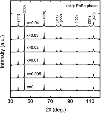 | ||
| Fig. 1 XRD spectra of PbSe:Alx samples with different Al concentrations of x = 0, 0.005, 0.01, 0.02, 0.03, and 0.04. | ||
Fig. 2a shows the plot of the room temperature Seebeck coefficient of Al doped PbSe as a function of carrier concentration. It is noted that the Seebeck coefficients of our PbSe:Alx (x = 0–0.03) samples are all negative showing the nature of n-type conduction. It was reported that indium could work as n-type dopant in PbSe.19,23 However, the reason is still unknown. We guess Al and In may get into the interstitial site, similar to Cu in Bi2Te2.7Se0.3, acting as n-type dopant.24 However, we did not observe any lattice parameter increase in Al-doped PbSe. A theoretical calculation clearly showed that Al replacing Pb is a reasonable result and causing both n-type conduction and resonant states.
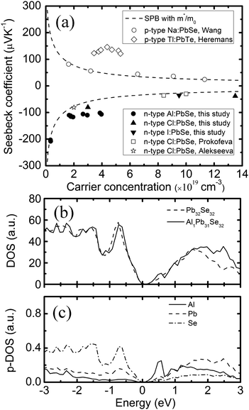 | ||
| Fig. 2 (a) Dependence of the Seebeck coefficient on the carrier concentration at RT. Solid lines are theoretical Pisarenko curves with m*/m0 = 0.28. Filled circles and triangles represent results of this study; (b) local DOS of Pb32Se32 and AlPb31Se32; (c) local p-DOS for each atom: Al, Pb, Se density of state of AlPb31Se32. A resonant state is shown near the conduction band edge of PbSe caused by Al. The valence band top is chosen as the zero energy in (b) and (c). | ||
The theoretical Pisarenko curves for both n- and p-type materials were calculated using a simple parabolic band model (SPB),25 as shown in eqn (1) and (2). We choose acoustic phonon scattering as the dominant electron scattering mechanism (r = −1/2), and the effective mass of m*/m0 = 0.28 according to PbSe:Na.17
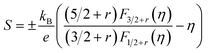 | (1) |
 | (2) |
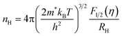
In eqn (1) and (2), S, kB, e, r, and RH are the Seebeck coefficient, Boltzmann constant, electron charge, scattering parameter, and Hall coefficient, respectively. The Fi(η) is the Fermi integral and η is the reduced Fermi energy. In Fig. 2a, the Seebeck coefficient of the pure PbSe sample (no Al added with a carrier concentration of ∼3.1 × 1018 cm−3), Cl-doped PbSe samples (0.2% and 1% Cl), I-doped PbSe sample (0.5% I) lies right on the n-type Pisarenko curve, indicating good agreement with the expectation of the SPB model. The reference samples with Cl18,23 for n-type and Na17 for p-type also fit the Pisarenko curve. In other words, there is no evidence of enhancement of the Seebeck coefficient by possible resonant states in normal n-type PbSe with Cl or I dopants. However, the situation for Al in PbSe is totally different: when the carrier concentration increases to 1.78–3.96 × 1019 cm−3 upon 0.5 to 3 at% Al doping, the Seebeck coefficient almost remains constant at around −115 μV K−1, about 40–100% higher than that from the SPB model and experimental values of PbSe:Cl samples with the same carrier concentration. Similar observation was also found in p-type PbTe:Tl samples,4 which was attributed to the increase of the local DOS near Fermi level by the presence of resonant states.
In order to find out which lattice site (Pb, Se, interstitial) in PbSe is more favourable for an Al atom and why the Seebeck coefficient remains the same with increased carrier concentration, we conducted first principles calculations based on density functional theory with a 2 × 2 × 2 super cell. Firstly, the formation energy of the two most possible cases, Al substituting Pb and the interstitial site, was calculated. The formation energy for the substitution case (AlPb31Se32) is defined as Esub = E(AlPb31Se32) − E(Pb31Se32) − E(Al), while for the interstitial case, it is Eint = E(AlPb32Se32) − E(Pb32Se32) − E(Al). Finally, we get the formation energy of substitution case (Esub = −0.45 Ry) lower than that of the interstitial case (Eint = −0.18 Ry), which means that the substitution case is more energy favourable. Based on the band structure calculation, the density of states (DOS) for both substitution and interstitial case was obtained. A small bump near the conduction band is found in the substitution case as compared with the un-doped case as shown in Fig. 2b. A partial DOS for each atom including Al, Pb, and Se is shown in Fig. 2c. A similar resonant state was also observed in Al-doped Pb1−xAlxTe.26,27 It is clearly suggested that a resonant state in the conduction band is caused by the 1.5% Al in Pb1−xAlxSe. However, we did not observe a similar resonant state near the band edge in the interstitial case (i.e., AlPb32Se32) according to our first principles calculation. Combining the experimental and theoretical results, we come to a conclusion that Al likely replaces Pb rather than sitting at the interstitial site.
It is reported that the modification of the band edge also can be realized by nanoinclusion,28,29 such as the AgSbTe2 nanoinclusion in the PbTe matrix.30 Since such nanoinclusions are widely observed in nanocomposites made by ball milling and hot pressing,3,21,22 the Al related nanoinclusion may be another possible reason for the unchanged Seebeck coefficient with increasing carrier concentration. Besides the possible band structure changing by resonant state or nanoinclusion, there is another possibility, i.e., an increase in scattering parameter r. This possible reason for the enhanced Seebeck coefficient can be interpreted from the Mott expression of Seebeck coefficient which is shown as following,
 | (3) |
The detailed thermoelectric properties of PbSe:Al samples are presented in Fig. 3 together with the data of the 0.2% Cl-doped PbSe sample for comparison. The Cl-doped PbSe is made by using the same method. It is found that Al is a much weaker n-type dopant than Cl. The carrier concentration (3.0 × 1019 cm−3) of 0.2% Cl-doped PbSe is comparable to that (2.7–2.9 × 1019 cm−3) of 2% Al-doped PbSe. However, the Seebeck coefficient (−80 μV K−1) of the 0.2% Cl-doped PbSe is much lower than that (−106 μV K−1) of the 2% Al-doped PbSe, which demonstrates that PbSe:Al has a larger effective mass than the 0.2% Cl-doped PbSe. This fact could be direct evidence for the existence of a resonant state. Owing to the enhanced Seebeck coefficient, a significantly higher power factor of 2030 μW m−1K−2 was obtained in the 2% Al-doped PbSe compared with 1440 μW m−1K−2 for the 0.2% Cl-doped PbSe.
 | ||
| Fig. 3 Temperature dependent thermoelectric properties of PbSe:Alx (x = 0, 0.005, 0.01, 0.02, and 0.03), (a) electrical resistivity, (b) Seebeck coefficient, and (c) power factor. The inset of (a) is the electrical resistivity of the pure PbSe sample without Al dopant. The dashed line is for the 0.2% Cl-doped PbSe. | ||
Total thermal conductivities of the studied samples, shown in Fig. 4, are calculated using κ = ρDCp, where ρ is the volumetric density, D the diffusivity (Fig. 4a), and Cp the specific heat (inset in Fig. 4a). In calculating κ, the Cp values of x = 0.01 are used for x = 0.005 and 0.01 samples, and that of x = 0.03 are used for x = 0.02 and 0.03 samples in a conservative way. The thermal conductivity of PbSe:Al samples are ∼0.9 W m−1 K−1 at 850 K. The lattice thermal conductivity is calculated by subtracting the electronic contribution from the total thermal conductivity (κlat = κ − κcarr = κ − LσT, where L is the Lorenz number). Here, the Fermi energy related Lorenz number is calculated by using the Fermi energy extracted from the Seebeck coefficient within a simple parabolic band model, and the acoustic phonon scattering as the major carrier scattering mechanism.31 As a result, the Lorenz number at room temperature ranges from 1.61 × 10⁻⁸ to 1.87 × 10⁻⁸ V2K−2 depending on the Al concentration. The κlat of the pure PbSe sample at RT is 1.81 W m−1 K−1, consistent with the reported data.17 The κlat of Al-doped samples is lower and decreases with Al concentration. It is very interesting to note that the Al-doped samples have κlat as low as 0.58–0.69 W m−1 K−1 at 850 K. This low κlat is related to the microstructures discussed below. The highest ZT of around 1.3 is achieved with x = 0.01 at 850 K, which is ∼300% and 40% higher than that of the un-doped and Cl-doped samples, respectively.
 | ||
| Fig. 4 Temperature dependent thermoelectric properties of PbSe:Alx (x = 0, 0.005, 0.01, 0.02, and 0.03), (a) diffusivity coefficient with the specific heat Cp as the inset, (b) thermal conductivity with the lattice thermal conductivity as the inset, and (c) figure of merit. The dashed line is for the 0.2% Cl-doped PbSe. | ||
In order to elucidate the reasons for such a low lattice thermal conductivity of PbSe:Al samples, extensive microscopy study was conducted by SEM and TEM. The following microscopic characteristics could be essential to theoretically explain the ultra-low lattice thermal conductivity. Firstly, the SEM microphotograph in Fig. 5a shows that the average grain size of PbSe:Al samples is less than 1 μm, which was analyzed by the linear intercept particle size analysis,32 and confirmed by the TEM bright field image shown in Fig. 5b. Secondly, Fig. 5a and b show that there are many nanosized pores (sphere-like, around 50 nm in diameter) distributing along the grain boundaries (mostly) and inside the grains (some), with the latter pores indicated by arrows in Fig. 5a and b. These small crystalline grains and the nanosized pores could mainly result in the reduced lattice thermal conductivity due to strong scattering of the phonons. Thirdly, it is interesting to observe that there are a lot of Pb-depleted disks with diameter around 2–5 nm and thickness less than 0.5 nm lying in the {100} planes in PbSe:Al grains, as shown in Fig. 5c. With a volumetric density of about 9 × 1017 cm−3, the Pb-depleted disks in Fig. 5c may cause significant lattice strain fields (3–20 nm) on both sides of the disks along their normal directions (see the arrow directions). This kind of Pb-depleted disks has been reported in our previous work33 in the PbTe system. Due to the lack of Pb atomic layers in the crystal, both the disks and the related lattice strain fields could also exert additional scattering effect on phonon transporting and lead to the reduced lattice thermal conductivity. Fourthly, the atomic scale microphotographs in Fig. 5d and e clearly show the contrast differences related to atomic columns and even a tilt contrast column, as separately pointed out by the arrows in Fig. 5e. Although Fig. 5e is only a modified HRTEM lattice image rather than a structural image, it is suggested that these weaker white spots were caused by the Al dopant. Accordingly, the atomically scaled inhomogeneity might affect the phonon scattering in each grain. Finally, along the [111] direction, Fig. 5f shows that there are many distinctive lattice areas, named subgrains (enclosed by white circles), in each grain. It is noted that these nanoscaled subgrains are separated by obscure boundary regions. It is suggested that these subgrain boundaries may come from the ball milling and hot pressing process.
 | ||
| Fig. 5 (a) SEM microphotograph of the freshly fractured surface, (b) the bright field TEM image of the typical PbSe:Al microstructure, (c) the HRTEM image of the Pb-depleted disks lying in the {100} crystal planes, (d) the atomic scaled lattice image showing the edge of crystal foil in (c), (e) the enlarged and modified HRTEM image from (d), and (f) nanoscaled subgrains and the subgrain boundaries. | ||
Conclusions
In summary, with the enhancement of the Seebeck coefficient due to the increase of the local DOS near Fermi level by possibly Al created resonant states, and the reduction of the lattice thermal conductivity by numerous distinctive microstructures, such as Pb depleted discs, small grains, and ∼10 nm subgrains, we report an enhanced ZT ≈ 1.3 at 850 K, which is ∼300% and ∼40% higher than the undoped and Cl-doped PbSe samples, respectively. By accurately controlling the alignment between the Fermi level and resonant states through other more appropriate dopants, further improvement of power factor and ZT could be expected.Acknowledgements
The work is partly funded by the US Department of Energy under contract number DOE DE-FG02-08ER46516 (QYZ and ZFR) and partly by the “Solid State Solar-Thermal Energy Conversion Center (S3TEC)”, an Energy Frontier Research Center funded by the U.S. Department of Energy, Office of Science, Office of Basic Energy Science under award number DE-SC0001299/DE-FG02-09ER46577 (GC and ZFR).References
- G. J. Snyder and E. S. Toberer, Nat. Mater., 2008, 7, 105–114 CrossRef CAS
.
- G. Chen, M. S. Dresselhaus, G. Dresselhaus, J. P. Fleurial and T. Caillat, Int. Mater. Rev., 2003, 48, 45–66 CrossRef CAS
- B. Poudel, Q. Hao, Y. Ma, Y. C. Lan, A. Minnich, B. Yu, X. Yan, D. Z. Wang, A. Muto, D. Vashaee, X. Y. Chen, J. M. Liu, M. S. Dresselhaus, G. Chen and Z. F. Ren, Science, 2008, 320, 634–638 CrossRef CAS
- J. P. Heremans, V. Jovovic, E. S. Toberer, A. Saramat, K. Kurosaki, A. Charoenphakdee, S. Yamanaka and G. J. Snyder, Science, 2008, 321, 554–557 CrossRef CAS
- Y. Pei, X. Shi, A. LaLonde, H. Wang, L. Chen and G. J. Snyder, Nature, 2011, 473, 66–69 CrossRef CAS
- J. P. Heremans, C. M. Thrush and D. T. Morelli, Phys. Rev. B: Condens. Matter Mater. Phys., 2004, 70, 115334 CrossRef
- J. Martin, L. Wang, L. Chen and G. S. Nolas, Phys. Rev. B: Condens. Matter Mater. Phys., 2009, 79, 115311 CrossRef
- S. V. Faleev and F. Leonard, Phys. Rev. B: Condens. Matter Mater. Phys., 2008, 77, 214304 CrossRef
- W. S. Liu, L. D. Zhao, B. P. Zhang, H. L. Zhang and J. F. Li, Appl. Phys. Lett., 2008, 93, 042109 CrossRef
- V. I. Kaidanov, S. A. Nemov and Y. I. Ravich, Sov. Phys. Semiconduct.-USSR, 1992, 26, 113–125 Search PubMed
- M. Zebarjadi, G. Joshi, G. H. Zhu, B. Yu, A. Minnich, Y. C. Lan, X. W. Wang, M. Dresselhaus, Z. F. Ren and G. Chen, Nano Lett., 2011, 11, 2225–2230 CrossRef CAS
- K. Biswas, J. Q. He, Q. C. Zhang, G. Y. Wang, C. Uher, V. P. Dravid and M. G. Kanatzidis, Nat. Chem., 2011, 3, 160–166 CrossRef CAS
- P. F. R. Poudeu, J. D'Angelo, A. D. Downey, J. L. Short, T. P. Hogan and M. G. Kanatzidis, Angew. Chem., Int. Ed., 2006, 45, 3835–3839 CrossRef CAS
- K. F. Hsu, S. Loo, F. Guo, W. Chen, J. S. Dyck, C. Uher, T. Hogan, E. K. Polychroniadis and M. G. Kanatzidis, Science, 2004, 303, 818–821 CrossRef CAS
- J. Androulakis, C. H. Lin, H. J. Kong, C. Uher, C. I. Wu, T. Hogan, B. A. Cook, T. Caillat, K. M. Paraskevopoulos and M. G. Kanatzidis, J. Am. Chem. Soc., 2007, 129, 9780–9788 CrossRef CAS
- D. Parker and D. J. Singh, Phys. Rev. B: Condens. Matter Mater. Phys., 2010, 82, 035204 CrossRef
- H. Wang, Y. Z. Pei, A. D. LaLonde and G. J. Snyder, Adv. Mater., 2011, 23, 1366–1370 CrossRef CAS
- G. T. Alekseeva, E. A. Gurieva, P. P. Konstantinov, L. V. Prokofeva and M. I. Fedorov, Semiconductors, 1996, 30, 1125–1127 Search PubMed
- J. Androulakis, Y. Lee, I. Todorov, D. Y. Chung and M. Kanatzidis, Phys. Rev. B: Condens. Matter Mater. Phys., 2011, 83, 195209 CrossRef
- A. D. LaLonde, Y. Pei and G. J. Snyder, Energy Environ. Sci., 2011, 6, 2090–2096 Search PubMed
- X. Yan, G. Joshi, W. S. Liu, Y. C. Lan, H. Wang, S. Y. Lee, J. W. Simonson, S. J. Poon, T. M. Tritt, G. Chen and Z. F. Ren, Nano Lett., 2008, 11, 556–560 CrossRef
- B. Yu, Q. Y. Zhang, H. Wang, X. W. Wang, H. Wang, D. Z. Wang, H. Z. Wang, G. J. Snyder, G. Chen and Z. F. Ren, J. Appl. Phys., 2010, 108, 016104 CrossRef
- L. V. Prokofeva, E. A. Gurieva, S. M. Zhumaksanov, P. P. Konstantinov, K. R. Mailina, Y. I. Ravich and L. S. Stilbans, Sov. Phys. Semiconduct.-USSR, 1987, 21, 1078–1080 Search PubMed
- W. S. Liu, Q. Y. Zhang, Y. C. Lan, S. Chen, X. Yan, Q. Zhang, H. Wang, D. Z. Wang, G. Chen and Z. F. Ren, Adv. Energy Mater., 2011, 1, 577–587 CrossRef CAS
- A. F. May, E. S. Toberer, A. Saramat and G. J. Snyder, Phys. Rev. B: Condens. Matter Mater. Phys., 2009, 80, 125205 CrossRef
- K. Xiong, G. Lee, R. P. Gupta, W. Wang, B. E. Gnade and K. Cho, J. Phys. D: Appl. Phys., 2010, 43, 4050403 Search PubMed
- A. N. Veis and Y. V. Glebova, Izv. Vyssh. Uchebn. Zaved., Fiz., 1983, 26, 117–119 CAS
- A. Popescu and L. M. Woods, Appl. Phys. Lett., 2010, 97, 052102 CrossRef
- Z. Y. Fan, H. Q. Wang and J. C. Zheng, J. Appl. Phys., 2011, 109, 073713 CrossRef
- Y. Zhang, X. Z. Ke, C. F. Chen, J. H. Yang and P. R. C. Kent, Phys. Rev. Lett., 2011, 106, 206601 CrossRef
- W. S. Liu, B. P. Zhang, J. F. Li, H. L. Zhang and L. D. Zhao, J. Appl. Phys., 2007, 102, 103717 CrossRef
- M. Brieseck, W. Lengauer, B. Gneiss, K. Wagner and S. Wagner, Microchim. Acta, 2010, 168, 309–316 CrossRef CAS
- H. Z. Wang, Q. Y. Zhang, B. Yu, H. Wang, W. S. Liu, G. Chen and Z. F. Ren, J. Mater. Res., 2011, 26, 912–916 CrossRef CAS
| This journal is © The Royal Society of Chemistry 2012 |